Experimental and theoretical investigations of
electronic and atomic structure of Si-nanocrystals
formed in sapphire by ion implantation
To cite this article: D Wainstein et al 2008 J. Phys.: Conf. Ser. 100 072014
View the article online for updates and enhancements.
Related content
Charging characteristics of Si nanocrystals embedded within SiO2 in the presence of near-interface oxide traps
V Ioannou-Sougleridis and A G Nassiopoulou
-Electroluminescence of Si Nanocrystal-Doped SiO2
Chen Dan, Xie Zhi-Qiang, Wu Qian et al.
-The electron and crystalline structure features of ion-synthesized
nanocomposite of Si nanocrystals in Al2O3
matrix revealed by electron spectroscopy
A Kovalev, D Wainstein, D Tetelbaum et al.
-Recent citations
Complex investigation of electronic structure transformations in Lead Sulphide nanoparticles using a set of electron spectroscopy techniques
A. Kovalev et al
-Investigation of anomalous physical properties of multilayer nanolaminate (TiAl)N/Cu coatings by electron spectroscopy techniques
Anatoly Kovalev et al
Experimental and theoretical investigations of electronic and
atomic structure of Si-nanocrystals formed in sapphire by ion
implantation
D Wainstein1, A Kovalev1, D Tetelbaum1, A Mikhailov1, C Bulutay2, A Aydinli2
1 Surface Phenomena Researches Group, 2-nd Baumanskaya str. 9/23,CNIICHERMET, office 475, Moscow, 105005 Russia
2 Department of Physics and National Nanotechnology Research Center, Bilkent University, Ankara, 06800 Turkey
E-mail: [email protected]
Abstract. The semiconductor nanocomposites based on Si nanocrystals in dielectric matrices attract a great amount of attention due to their ability for luminescence in visible and near-IR part of the electromagnetic spectrum. Si nanocrystals in sapphire matrix were formed by Si+ ion implantation with doses from 5x10¹⁶ to 3x1017 cm-2 at an accelerating voltage 100 kV and post-implantation annealing at 500 - 1100 oC for 2 hours. Depth distribution of lattice defects, impurities and Si nanocrystals, the peculiarities of interband electronic transitions were investigated by XPS and HREELS. The molecular orbitals and local electronic structure of the Al2O3 matrix with Si nanocrystals was calculated using an atomistic pseudopotential technique. The electronic structure of Si nanocrystals as determined from HREELS measurements is in good agreement with the theoretically calculated electronic structure for Si nanocrystals.
1. Introduction
Development of the silicon-based optoelectronics (including light-emitting devices) is now a very important scientific and technology task. One of the ways for the introduction of silicon into the family of the light-emitting (optoelectronic) materials is using the remarkable property of nanocrystals (quantum dots): the possibility of the quasi-direct radiative transitions of electrons instead of indirect band–gap transition in bulk silicon. This property is caused by the effect of so-called quantum confinement. It was shown that if silicon nanocrystals with the size of 2 –5 nm are embedded into the SiO2 matrix (SiO2:Si), rather strong luminescence in the visible range of spectrum is observed at room temperature [1]. The development of nanocomposites on basis of Al2O3 matrix allows to fabricate heat resistant and radiation resistant semiconductors.
The ion implantation is one of the best methods for the fabrication of Al2O3:Si composites due to its excellent compatibility with usual planar microelectronic technology. The significant success is already achieved in the obtaining visible luminescence in SiO2:Si produced by this method [2-3]. However, important scientific problems arise on the way to wide employment of the ion implantation for the Al2O3:Si fabrication.
One of the primary goals in the studying size-confined systems is to understand the evolution of electronic structure with size. As a result, much effort has gone into measuring the electronic structure
IVC-17/ICSS-13 and ICN+T2007 IOP Publishing
of nanocrystals by electron spectroscopy, which has been successful in yielding extremely sophisticated information about transitions at or near the energy gap. XPS and HREELS techniques have the potential of acquiring information about the bands of a different nature, namely, the density of occupied and unoccupied states. Here we present an experimental and theoretical study of light emitting Si-NC embedded in Al2O3.
2. Experimental details
Materials. The polished sapphire single crystal samples R(1102) orientation, 10x5x1 mm were implanted 100 keV by Si+ with doses from 5x10¹⁶ to 3x1017 cm-2. The samples were annealed at 500 — 1100 оС for 2 hours in N2 atmosphere to form Si nanoinclusions in surface layers.
Methods. The research was carried out on the electron spectrometer ESCALAB MK2 (VG) with Al Kα X-ray monochromatized source (hν = 1486.6 eV) in vacuum of 1x10⁻⁸ Pa. As prepared samples and samples that were multiple etched with an Ar+ gun were investigated.
The High Resolution Electron Energy Losses Spectroscopy (HREELS) was used for investigation of interband transitions between the conducting band and the valence band of nanocrystals and estimation of Si nanocrystal electronic structure features. The HREEL spectra were recorded at primary beam energy 30.0 eV, at 50o angle of incidence with respect to the surface normal.
3. Theoretical details
An atomistic pseudopotential technique is developed [4] to study the electronic structure and interband transitions of Si-nc embedded in Al2O3 matrix. Any imperfections in the crystalline order in both the core and matrix are ignored as well as strain effects. This enables us to identify features due to such imperfections like F-centers that are only present in the experimental spectra. The electronic structure, density of states are obtained for several NC diameters. The imaginary part of the optical dielectric function, Im{ε(ω)} is computed within the independent particle approximation. This is in turn used to calculate its real part through the Kramers-Kronig relation which then yields the energy loss function, Im{-1/ε(ω)}. This theoretical study becomes instrumental in the interpretation of the HREELS data.
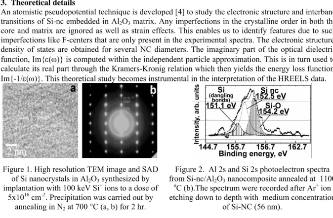
Figure 1. High resolution TEM image and SAD of Si nanocrystals in Al2O3 synthesized by implantation with 100 keV Si+ ions to a dose of
5x1016 cm-2. Precipitation was carried out by annealing in N2 at 700 °C (a, b) for 2 hr.
Figure 2. Al 2s and Si 2s photoelectron spectra from Si-nc/Al2O3 nanocomposite annealed at 1100
oC (b).The spectrum were recorded after Ar+ ion etching down to depth with medium concentration
of Si-NC (56 nm). 4. Results and Discussion
The detailed information about the structure of Si-nc/Al2O3 nanocomposite was obtained by high resolution TEM. A complex Si-NC in Al2O3 structure appears from the analysis of the high resolution image (Figure 1). In particular, the presence of the Si (111) reflection on diffraction patterns of Figure 1, b and visible (111) planes on TEM indicate the presence of a crystalline particle. Furthermore, this nanocrystal is surrounded by an external shell about 1 nm thick with the absence of reticular planes. The sapphire matrix has a partly amorphous structure under 700 oC annealing, and it is recrystallized after heating to 1050 oC. Size of Si nanocrystals grows from 2 nm to 4-5 nm when annealing temperature changes from 700 to 1050 oC. The PL from Si nanocrystals was observed at 780 nm
(λex=337 nm) after Si+ ion implantation with dose 5·1016 cm-2 at 100 kV. The intensity of this peak was decreased with increasing of dose and accelerating voltage of Si ion implantation.
XPS depth profiling performed by Ar+-ion etching found the non-uniform distribution of Si in the implanted sapphire layer. Si distribution has a maximum at the depth of about 84-100 nm and remains unchanged with the annealing temperature increase at least to 1100 oC.
The XPS spectrum of Si+-implanted (5·1016 cm-2) sapphire samples after annealing at 1100 oC is presented on the Figure 2. It was recorded after Ar+ ion etching to 56 nm depths. The position of the Si 2s line at 151.7 eV and its additional component at 154.2 eV are shifted from the binding energy value of bulk Si = 151.0 eV evidences the presence of Si nanocrystals and partial oxidation of Si atoms at interfaces. We observed the size-dependent shift +0.7 eV of the Si nanocrystal component of the Si 2s photoelectron line that was described in [5].
Analysis of Si oxidized atom concentration follows the estimation of the fraction of nanocrystal surface atoms. Assuming the spherical shape of the crystals, we can calculate the dependence of its diameter from the etching depth (Table 1).
Table 1. Dependence of Si-NC diameter as a function of depth in Si-NC/Al2O3 sample after annealing at 1100 oC (on base of XPS depth profiling).
Depth, nm 28 42 56 70 84 98
Si-NC diameter, nm 2.0 2.6 3.8 4.5 5.5 4.5
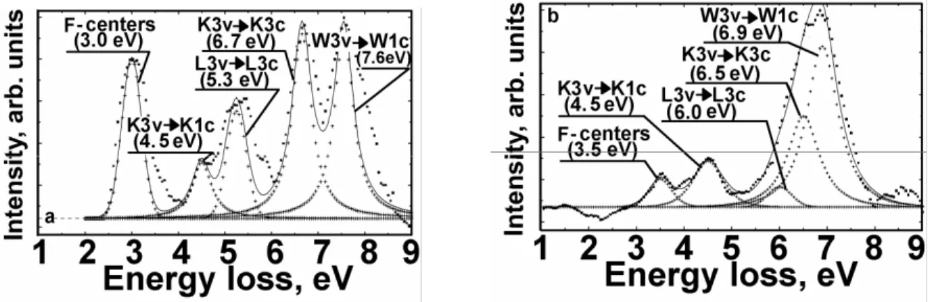
The interband transition analysis is very important for investigations of band gap features in semiconductors and density of states above Fermi level. The peak at energy 3.0-3.5 eV in Figure 3 is connected with F-centers in Al2O3 matrix. The F-center is an oxygen vacancy occupied by two electrons. It is formed due to implantation of Si+ ions into crystalline lattice of sapphire. Intensity of the 3.0 eV peak does not change at all depths of etching, for samples annealed at 500 oC. But annealing at higher temperatures results in decreasing point defect concentration. So the peak at 3.0 – 3.5 eV associated with F-centers presented on Figures 3, a-b decreases with elevation of annealing temperature, and it practically disappears after an 1100 oC annealing.
The peaks at 4.0-9.0 eV are associated with excitation of electron transitions through the band gap. Comparing experimental HREEL spectra with the theoretical analysis, we can attribute the individual loss peaks on spectra of Figure 3, a - b with the Si nanocrystals and the Al2O3 matrix.
Figure 3. HREEL spectra from Si-NC/Al2O3 nanocomposite annealed at 1100 oC .The spectra were recorded after Ar+ ion etching on depth with maximal concentration of Si-nanocrystals (84 nm). a - annealing at 700 oC; diameter of Si NC is 2.0 nm (TEM); b - annealing at 900 oC; diameter of Si
NC is 3.5 nm (XPS).
IVC-17/ICSS-13 and ICN+T2007 IOP Publishing
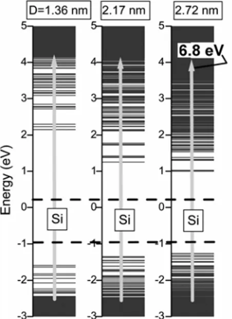
Figure 4 shows the variation of the Si NC states with respect to size; the band gap gradually approaches to that of the bulk as the diameter increases. This theoretical value correlates very well with the highest peak registered in the EEL data in Figure 4, b. The most conclusive evidence comes from Figure 5 that shows the theoretical prediction of EEL for a 3.5 nm Si NC embedded in a perfect Al2O3 lattice. The peak around 4.5 eV is unambiguously due to NCs, as it disappears in their absence as indicated by the dashed line. The other main peak around 7 eV is clearly due to Al2O3 matrix which is reproduced by the NC-free curve. It should be stressed that there is no fitting parameter in our theory, hence the agreement with experiment is quite meaningful.
Fig.4. Molecular orbital levels of Si NC at three different diameters. The dotted lines are marked
as the band gap of bulk Si
Fig. 5. Calculated energy loss function for 3.5 nm Si nanocrystals in Al2O3 matrix; the dashed line
shows the case without the presence of NCs.
5. Conclusions.
The electronic structure of inner and outer shells of Si nanocrystals in sapphire depends from NCs size. These data were obtained by complex investigations using TEM, XPS, HREELS, EELFS and electronic structure calculations. The theoretical calculations are in very good agreement with experimental results.
Acknowledgements. The work was partly supported by the European Commission through the FP6 project SEMINANO Contract No: NMP4-CT-2004-505285, and by RF State Contract 3662p/4844 provided by FASIE.
References
[1] Canham L.T. Appl. Phys. Lett., 1990, V. 57, p. 1046.
[2] Tetelbaum D.I., Gorshkov O.N., Filatov D.O., Kasatkin A.P., Novikov V.A., Trushin S.A., Stepichova M.V. In: International workshop on nondestructive testing and computer simulations in science and engineering, Alexander I. Melker, Editor, Proceedings of SPIE. 1999, V.3687, p.258.
[3] Kovalev A.I., Wainstein D.L., Tetelbaum D.I., Thin Solid Films. 2006, 515, p. 591-595. [4] Bulutay C., Physica E, 38 (2007) 112-117.
[5] Chang Q. Sun,* B. K. Tay, Y. Q. Fu, S. Li, T. P. Chen, H. L. Bai and E. Y. Jiang, J.Phys. Chem. B, 107 (2003) 411-414.
[6] Alivisatos A.P., Science 271, 933 (1996).
[7] Bawendi M. G., Steigerwald M. L., and Brus L. E., Ann. Rev. Phys. Chem.1990, 41, p. 477.
IVC-17/ICSS-13 and ICN+T2007 IOP Publishing
Journal of Physics: Conference Series 100 (2008) 072014 doi:10.1088/1742-6596/100/7/072014