FABRICATION OF AN ON-CHIP
NANOWIRE DEVICE WITH
CONTROLLABLE NANOGAP FOR
MANIPULATION, CAPTURING, AND
ELECTRICAL CHARACTERIZATION OF
NANOPARTICLES
A THESIS
SUBMITTED TO THE DEPARTMENT OF ELECTRICAL AND ELECTRONICS ENGINEERING
AND THE INSTITUTE OF ENGINEERING AND SCIENCES OF BILKENT UNIVERSITY
IN PARTIAL FULLFILMENT OF THE REQUIREMENTS FOR THE DEGREE OF
MASTER OF SCIENCE
By
Can Uran
August 2008
ii
I certify that I have read this thesis and that in my opinion it is fully adequate, in scope and in quality, as a thesis for the degree of Master of Science.
Assist. Prof. Dr. Hilmi Volkan Demir (Supervisor)
I certify that I have read this thesis and that in my opinion it is fully adequate, in scope and in quality, as a thesis for the degree of Master of Science.
Assist. Prof. Dr. Ali Kemal Okyay
I certify that I have read this thesis and that in my opinion it is fully adequate, in scope and in quality, as a thesis for the degree of Master of Science.
Assist. Prof. Dr. Uygar Tazebay
Approved for the Institute of Engineering and Sciences:
Prof. Dr. Mehmet B. Baray
iii
ABSTRACT
FABRICATION OF AN ON-CHIP NANOWIRE DEVICE
WITH CONTROLLABLE NANOGAP FOR
MANIPULATION, CAPTURING, AND ELECTRICAL
CHARACTERIZATION OF NANOPARTICLES
Can Uran
M.S. in Electrical and Electronics Engineering Supervisor: Assist. Prof. Dr. Hilmi Volkan Demir
August 2008
One of the major challenges in nanofabrication commonly arises from the necessity to integrate nanostructures (e.g., nanoparticles) on the same chip with microcomponents (e.g., microelectrodes) that are orders-of-magnitude larger in size. For example, in order to make electrical contacts to colloidally synthesized nanoparticles (typically 1-100 nm in size) by integrating them with microelectrodes (typically in the few micrometers range on the critical side), a large size mismatch that easily ranges from 1:10 to 1:10,000 is required to be handled delicately for successful nano-to-micro integration. This necessitates the ability to manipulate and integrate nanoparticles with a sufficient level of precision on the microchip. In this thesis, to provide a convenient solution to this challenging problem, we proposed and demonstrated for the first time an on-chip nanowire device that features a controllable nanogap in its architecture for capturing and electrical characterization of nanoparticles in the gap, all fully integrated on the same microchip. Our innovative approach relies on the use of dielectrophoretic electric-field assisted self-assembly of our segmented nanowires to construct a nanoscale device platform. For this purpose, we synthesized gold-silver-gold segmented nanowires and dielectrophoretically aligned them across our microfabricated array of electrodes. Subsequently, we selectively removed the middle silver segment to open a gap in the nanometer
iv
size between the self-aligned gold end segments. Using dielectrophoretic assembly once more, we captured nanoparticles in these nanogaps for further electrical characterization. One of the key benefits in our approach was that the aligned nanowires automatically provided electrical contacts to the captured nanoparticles to allow for electrical probing at the nanoscale. Our innovative approach enabled convenient full integration from nanoparticles to nanowires to microelectrodes to macroprobes on a single chip, spanning a size range of more than six orders of magnitude.
v
ÖZET
NANOPARÇACIKLARIN YÖNLENDĐRĐLMESĐ,
YAKALANMASI VE KARAKTERĐZASYONU ĐÇĐN
YAPISINDA KONTROLLÜ NANOBOŞLUK
BULUNDURAN ÇĐP ÜZERĐNDE NANOTEL AYGITI
FABRĐKASYONU
Can UranElektrik Elektronik Mühendisliği Yüksek Lisans Tez Yöneticisi: Yar. Doç. Dr. Hilmi Volkan Demir
August 2008
Nanofabrikasyonda başlıca sorunlardan biri nano yapıların (örneğin, nanoparçacıkların) mikro elemanlar (örneğin, mikroelektrotlar) ile aynı çip üzerinde tümleştirme ihtiyacından kaynaklanmaktadır. Örneğin, koloidal nanoparçacıklara (tipik olarak 1-100 nm boyutlarında) mikroelektrotlar (tipik olarak birkaç mikrometre boyutlarında) ile entegre edilmeleriyle elektriksel kontak sağlamada, boyutta 1:10’dan 1:10,000’e varan nano-mikro entegrasyon için incelikle ele alınması gereken bir boyut uyumsuzluğu vardır. Bu sorun, nanoparçacıkların yeterli derecede hassasiyet ile yönlendirilebilmesini ve diğer yapılara entegre edilmesini gerektirir. Bu tezde, bu soruna kullanışlı bir çözüm getirmek üzere nanoparçacıkların karakterizasyonu için, yapısında kontrollü nanoboşluk bulunduran, çip üzerinde nanotel aygıtı ilk defa önerdik ve gerçekleştirdik. Yenilikçi yaklaşımımız, nanoboyutta aygıt platformu yapımı için, bölmeli nanotellerin dielektoroforetik elektriksel alan kullanımı ile dizilmesine dayanmaktadır. Bu amaçla, altın-gümüş-altın bölmeli nanoteller sentezledik ve bunları mikro boyutta ürettiğimiz elektrot dizinlerine dielektroforetik yöntem ile yerleştirdik. Bunu takiben, kendiliğinden hizzalı iki uç altın bölme arasında nanoboşluk açmak için, seçici olarak ortadaki gümüş bölmeyi kaldırdık. Bir kez daha dielektroforetik yerleştirme kullanarak,
vi
karakterize edilmek üzere nanoboşluklarda nanoparçacıklar yakaladık. Yaklaşımımızın önemli faydalarından biri, dizdiğimiz nanotelleri yakalanan nanoparçacıklara kendiliğinden, nano ölçekte problamaya izin vererek elektrik kontak sağlamasıdır. Yenilikçi yaklaşımımız nanoparçacıklardan nanotellere, nanotellerden mikroelektrotlara, ve mikroelektrotlardan makroproblara, boyutta milyonlarca kat mertebesinde bir aralığı kapasayarak tek bir çip üzerinde bütün bir entegreye olanak sağlamaktadır.
vii
Acknowledgements
First of all, I would like to thank my supervisor Prof. Hilmi Volkan Demir, who has provided me with the understanding, discipline and motivation in both scientific study and life. His kind, friendly and motivated personality, guided me during my study of research and I am honored with his supervision. I thank him again for his endless effort and support on me.
I would like to thank Prof. Ali Kemal Okyay, and Prof. Uygar Tazebay for being my thesis committee and their valuable comments on my thesis work.
I would like to thank Emre Ünal for working together on this project and Prof. Ramazan Kızıl for providing his support.
I would like to thank all of my friends in our Sensors and Devices Research Group for their great support and unforgettable times together: Özgün Akyüz, Tuncay Özel, Emre Sarı, Sedat Nizamoğlu, Đlkem Özge Hüyal, Evren Mutlugün, Gülis Zengin, Rohat Melik, Dr. Nihan Kosku Perkgöz, Aslı Ünlügedik, Neslihan Çiçek, Gürkan Polat, Akın Sefünç, Onur Akın and our ex-members Murat Soğancı, Aslı Koç, Dr. Gülşah Yaman, and Sümeyra Tek.
I would like to thank all IAL, NANOTAM, and UNAM researchers and staff for their support and help on my experimental studies and for providing me a well equipped research environment.
I would like to thank all EE faculty, technical and administrative staff, researchers, and to my EA 229 officemates, Emre Kopanoğlu, Elif Aydoğdu, Kaan Oğuz, and Esra Abacı. I am really pleased to study in my department where I could easily establish very good relations, friendships and acquire high level of engineering education.
Lastly, I would like to thank a lot to my parents, my brother and all my family and friends for their love.
viii
Table of Contents
1. INTRODUCTION ...
2. OVERVIEW OF DIELECTROPHORESIS AND APPLICATIONS4
2.1 BACKGROUND ON DIELECTROPHORESIS... 4
2.1.1 DIELECTROPHORESIS... 4
2.1.2 ELECTROROTATION... 7
2.1.3 TRAVELLING WAVE DEP... 9
2.2 APPLICATIONS OF DIELECTROPHORESIS... 10
3. MICROELECTRODE ARRAY DESIGN AND FABRICATION.. 15
4. NANOWIRE SYNTHESIS... 25
4.1 NANOWIRE SYNTHESIS... 25
4.2 NANOGAP VARIATION STUDY... 34
5. OUR DIELECTROPHORESIS EXPERIMENTS... 37
5.1 DIELECTROPHORETIC ALIGNMENT OF OUR NANOWIRES... 37
5.2 CLAMPING OF THE NANOWIRES AND I-V CHARACTERIZATION... 39
5.3 NANOGAP FORMATION... 42
5.4 NANOPARTICLE CAPTURE... 44
ix
List of Figures
Figure 1.1 Our on-chip integration from macro to micro to nano scale... 3 Figure 2.1.1.1 Schematic diagram of the net force acting on a polarizable particle due to the interaction of induced charges and local electric field [1]... 5 Figure 2.1.2.1 The polarizable particle suspended in a rotating electric field generated by four electrodes with 90° phase difference. If the electric field moves fast enough, the induced dipole M will lag behind the field inducing a torque in the particle due to the interaction between electric fields and lagging dipole [1] ... 8 Figure 2.1.3.1 A particle is suspended in a travelling electric field generated by electrodes which are 90° out of phase. The electric field moves quickly that the induced dipole M falls behind the electric field, inducing the force F, causing the particles to move along the electrodes [1]... 9 Figure 3.1 represents exemplary simulation results of different electrode fingers ... 16 Figure 3.2 represents exemplary simulation results of different electrode fingers ... 16 Figure 3.3 represents exemplary simulation results of different electrode fingers ... 17 Figure 3.4 represents exemplary simulation results of different electrode fingers ... 17 Figure 3.5 represents exemplary simulation results of different electrode fingers ... 18 Figure 3.6 represents exemplary simulation results of different electrode fingers ... 18 Figure 3.7 Cross-sectional sketch of our device... 20 Figure 3.8 Mask design of lower and upper electrodes in (a) and (b), respectively... 20 Figure 3.9 Top view of optical microscopy image of two electrodes along with a zoom-in of lower electrodes ... 20 Figure 3.10 General top-view of one of our fabricated chips ... 22
x
Figure 3.11 A 3 µm x15 µm fingered electrode with a gap of 5 µm ... 22 Figure 3.12 Zoom-in of a 3 µm x15 µm fingered electrode with a gap of 5 µm ... 22 Figure 3.13 A 5 µm x15 µm fingered electrode with a gap of 5 µm ... 23 Figure 3.14 Zoom-in of a 5 µm x15 µm fingered electrode with a gap of 5 µm ... 23 Figure 3.15 A Fingerless electrode with a gap of 5 µm ... 24 Figure 3.16 Zoom-in of a fingerless electrode with a gap of 5 µm ... 24 Figure 4.1.1 Our own experimental setup for electrodeposition that includes template membrane disc, o-ring, and plates ... 26 Figure 4.1.2 Versastat3 potentiostat/galvanostat... 26 Figure 4.1.3 Experimental setup for electrodes... 27 Figure 4.1.4 Potential trace during silver deposition into the branched part of the alumina disc... 28 Figure 4.1.5 Potential trace during gold deposition into the pores of the alumina disc for Au segments of our nanowires ... 28 Figure 4.1.6 Potential trace during silver deposition into the pores of the alumina disc for Ag segments of our nanowires ... 29 Figure 4.1.7 Backside of the membrane disc (a) before deposition, (b) after silver backing, (c) after Au deposition, (d) after Ag deposition ... 30 Figure 4.1.8 SEM image of the nanowires inside the alumina disc ... 31 Figure 4.1.9 SEM image of an exemplary nanowire with a short Ag segment in the middle between long Au segments at the ends (with a total nanowire length of 7.78 µm) ... 32 Figure 4.1.10 SEM image of another nanowire with 3.23 µm and 3.35 µm long Au segments ... 32 Figure 4.1.11 Nanowires suspended in methanol... 33
xi
Figure 4.1.12 Optical image of our randomly distributed nanowires immobilized on substrate... 33 Figure 4.2.1 Gap length vs. charge. Blue points represent the lengths of Ag segments, and black lines represent the standard deviation among Ag segment lengths ... 34 Figure 4.2.2 Example of Au-Ag-Au segmented nanowires with varied Ag segment lengths of 300 nm, 200 nm, 100 nm, 50 nm, and 20 nm in (a), (b), (c), (d), and (e), respectively... 35 Figure 4.2.3 Gold nanoparticles in water ... 36 Figure 4.2.4 Absorbance spectrum of gold nanoparticles in film... 36 Figure 5.2.1 SEM image of the aligned and clamped Au-Ag-Au segmented nanowire, and its I-V plot in the inset ... 39 Figure 5.2.2 Optical image of the clamped nanowire ... 40 Figure 5.2.3 SEM image of the nanowire after aligned dielectrophoretically ... 41 Figure 5.2.4 SEM image of the aligned nanowire after clamping... 41 Figure 5.3.1 SEM images of the nanowire before and after nanogap formation in (a) and in (b), respectively... 42 Figure 5.3.2 SEM image of the nanowire after gap formation in the middle, and its I-V plot in the inset ... 43 Figure 5.4.1 SEM image of a nanoparticle trapped in nanogap dielectrophoretically ... 44 Figure 5.4.2 SEM image of a nanoparticle trapped in nanogap and its I-V in the inset ... 44 Figure 5.4.3 SEM images of (a) microelectrode fingers before nanowire alignment (along with their I-V showing open circuit in the inset), (b) aligned Au-Ag-Au segmented nanowire by using DEP and clamps (along with its I-V showing electrical conduction in the inset), (c) nanowire after gap formation in the middle (along with its I-V showing open circuit again in the inset), and finally (d) nanoparticles captured in the size controllable nanogap by using DEP (along with I-V showing electrical conduction in the inset)... 46
1
Chapter 1
Introduction
For the nanoscale construction, there are two principle approaches known as top-down and bottom up approaches. The top-down approach constructs smaller components from a larger piece. The bottom-up approach, on the other hand, constructs a larger structure by bringing smaller parts together. For that, the bottom-up approach facilitates self-assembly to build the components into functional architectures. However, the integration of macroworld to nanoworld is still a problem in nanofabrication. Manipulating particles and precise positioning at the nanoscale is of critical importance. Such micro-nano integration can be established by combining well-designed manipulation methods and interfacing or bridging components such as nanowires, combining the top-down and bottom-up approaches together. In this thesis, we investigate dielectrophoresis (DEP), which is an electric-field assisted self-assembly technique, to be used in alignment and integration of nanodevices and nanoparticles on micro-level platforms in the form of electrode arrays.
In our thesis, we focus on building an on-chip nanowire device for manipulating, capturing, and electrical characterization of nanoparticles. We study DEP-assisted manipulation of our Au-Ag-Au segmented nanowires that feature controllable nanogaps in their middles on pre-patterned microelectrodes. By selective etching of Ag, to build nanowire device in which nanoparticles can be captured and electrically characterized in the controllable sized nanogaps of large arrays of these nanowires. Achieving the dielectrophoretic manipulation of nanoparticles into the nanogaps located in the middle of these nanowires, which are aligned on the fingers of lithographically fabricated microelectrodes, and by
2
achieving electrical contact to them by macro-probes via nanowires aligned on microelectrodes, we show full integration from macroworld to nanoworld. In the following chapters, theoretical background on dielectrophoresis, our nanowire synthesis, microfabrication, device designs, experiments, and results are described. In chapter 2, we introduce DEP which stems from spatially non-uniform electric field where the induced moment is translated into a net force on polarized particles. We explain the dielectrophoretic force, its formalism and different kinds of motion of particles using dielectrophoresis, including capturing, rotation, travelling wave. We also present uses and applications of dielectrophoresis as an electric field assisted assembly method enabling to build different device platforms. We also introduce other applications of dielectrophoresis on particle separation, which is useful for biotechnological applications, including purification, fractionation, and concentration of cells and microorganisms.
In chapter 3, we explain the design and fabrication of the microelectrodes of our device platform. We describe the fabrication parameters and process of the microelectrodes enabling the conditions for dielectrophoresis manipulations for nanowires.
In chapter 4, we present the nanowire synthesis. We describe our template porous aluminum oxide membranes where we deposit our Au-Ag-Au segmented nanowires by chemical electrodeposition. By explaining our process steps, we explain the methods for synthesis and nanowire solution preparation where the nanowire suspension in liquid medium is used for dielectrophoresis. Our gap variation study, where we controllably deposit the mid Ag segment of our wires in defined size in nanometer scale and remove it by selective chemical etching to form nanogaps, is explained in this section.
In chapter 5, we describe our dielectrophoresis experiment parameters, setup, experimental results and characterization. We explain the steps building our device platform and our proof-of-concept demonstration to show that it allows for capturing and characterizing nanoparticles in the controllable sized nanogaps. We also present the SEM images and I-V characterizations of all
3
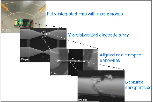
these steps which include: first the empty microelectrode fingers that we observe to be electrically open, second electrical conduction between the Au end of nanowires when we align the Au-Ag-Au segmented nanowires, third open circuit when we form nanogap by removing the Ag segment, and finally electrical conduction again between the Au ends of the nanowires after capturing of gold nanoparticles in the nanogaps by dielectrophoresis. In the final chapter, we conclude our discussions to show that we constructed a nanowire device platform (Figure 1.1).
4
Chapter 2
Overview of dielectrophoresis and
applications
2.1 Background on dielectrophoresis
2.1.1 Dielectrophoresis
Dielectrophoresis (DEP) stems from spatially non-uniform electric field, where the induced moment is translated into a net force on polarized particles. This can be used to manipulate particles, also in nanometer scale. Due to the field gradient, the dielectrophoretic forces generated as a result of the interaction of the applied electrical field with the induced charges are not equal on each side of the particles. This inhomogeneous nature of the electric field causes a net force towards the high field gradient (Figure 2.1.1.1) [1]. In operation, DEP facilitates capture, transport and rotation of particles, making use of both positive and negative dielectrophoretic effects. The DEP force strongly depends on the frequency applied of the non-uniform electric field, permittivites, conductivities of the host medium, and the particle, and also to the particle size [2].
5
Figure 2.1.1.1 Schematic diagram of the net force acting on a polarizable Particle due to the interaction of induced charges and local electric field [1].
In an electric field
E
r
, a particle behaves as a dipole with the dipole moment
m
r
, which is proportional to the electric field and this relation is given by [3]:( ) ( )
ω
ω
πε
ω
r K E m m r r 3 4 ) ( = (1)Under the effect of an electric field gradient, the force on the dipole is given by [4]:
( )
[
(
m( )
)
E]
F
ω
= Reω
∇ (2)Combining the two relations for a spherical particle of radius r and permittivity
εp, in the medium with the permittivity of εm, the dielectrophoretic force is given
by [4]:
[
]
rmsm
DEP
r
K
E
F
=
2
π
3ε
Re
(
ω
)
∇
2 (3)where εm is the permittivity of the medium, r is the particle radius, ω is the
angular frequency, and Erms is the root mean square electric field. K(ω) is the
Clausius-Mossotti function, which depends on the complex permittivities of the sphere particle and the medium via the equation:
6
( )
* * * *2
m p m pK
ε
ε
ε
ε
ω
+
−
=
(4) where ω σ εε*= − j , which is the complex permittivity.
The direction (positive or negative) of the force depends on the sign of the real part of the Clausius-Mossotti factor given by [5]:
( )
[
]
)
1
(
)
2
(
)
(
3
2
Re
2 2 2 MW m p MW m p p m m p m pK
τ
ω
σ
σ
τ
σ
ε
σ
ε
ε
ε
ε
ε
ω
+
+
−
+
+
−
=
(5)where εm and εp are permittivities of the medium and particle; σm and σp are
conductivities of the medium and particle, respectively. τMW = (εp+εm)/(σp+2σm)
is the time constant that characterizes the decay of a dipolar distribution of charge on the surface of a spherical particle.
The high and low frequency limits for the real part of the Clausius-Mossotti factor are given by:
Re[K(ω)] = (σp-σm) / (σp+2σm) for ωτMW <<1 (6)
Re[K(ω)] = (εp-εm) / (εp+2εm) for ωτMW >>1 (7)
In the case of εp>εm and σp<σm, Re[K(ω)] is negative at low frequencies and
positive at high frequencies.
In the case of εp<εm and σp>σm, Re[K(ω)] becomes positive at low frequencies
and negative at high frequencies. For metallic particles, where σp>>σm,
Re[K(ω)] is ~ 1 for low frequencies when ωτMW <<1.
The frequency dependency of the Clausius-Mossotti factor shows that dielectrophoretic force also has dependency on frequency. This factor also varies depending on whether the particle is more polarizable than the medium or
7
not, assigning the direction of the dielectrophoretic force. If Re[K(ω)] is positive, then the particles move to high field gradients. This is called positive dielectrophoresis. If Re[K(ω)] is negative, then the particles move to low field gradients, which is called negative dielectrophoresis [1].
The dielectrophoretic force depends on the induced dipole and responds only to the field gradient instead of the direction of the electric field. The magnitude of the∇E2rms, which determines strength of the DEP force, is greater around the
tips of the electrodes because of the non-uniform electric field distribution and there is a net force towards the electrodes where the electrical field gradient is maximum.
2.1.2 Electrorotation
In a rotating electric field, the induced dipole formed across the particle will rotate with the electric field. However, if the angular frequency of the field is sufficiently high, the dipole will lag behind to the field. This angle between the dipole and the field results in a torque causing the particle rotate (Figure 2.1.2.1) [1]. The torque on a spherical particle of radius r suspended in a rotating field E is:
( )
[
]
2 3Im
4
πε
mr
K
ω
E
rms−
=
Γ
(8)where Im[K(ω)] represents the imaginary component of the Clausius-Mossotti factor. The minus sign shows that the dipole moment rotates in the opposite direction of the applied field if Im[K(ω)] is positive.
Accounting for the effect of viscosity, η, the rotation rate is given by [6]:
8
First of the two major differences between the dielectrophoretic force and torque acting on the particle is that the torque is a function of the square of the electric field rather than gradient of the electric field square. Secondly, it depends on the imaginary part of the Clausius-Mossotti factor while the dielectrophoretic force depends on the real part of this factor.
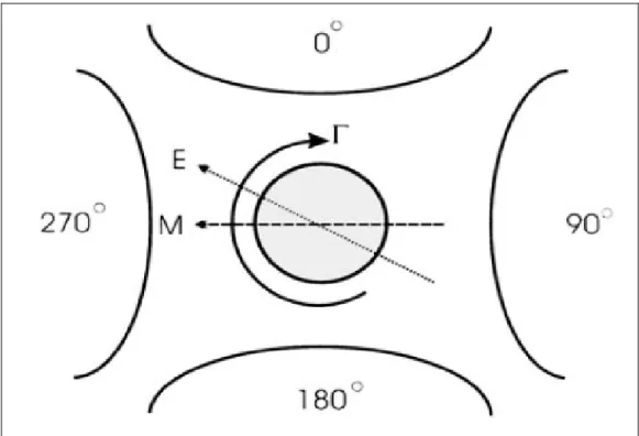
Figure 2.1.2.1 The polarizable particle suspended in a rotating electric field generated by four electrodes with 90° phase difference. If the electric field moves fast enough, the induced dipole M will lag behind the field inducing a torque in the particle due to the interaction between electric fields and lagging dipole [1].
9
2.1.3 Travelling wave DEP
Travelling wave DEP is a linear analogue of electrorotation such that electrodes are laid out as tracks, but each electrode being 90° advanced from the previous one. This phase difference between the electrodes creates an electric field which travels among the electrodes, resulting in the induction of a force manipulating the particles to move along the electrodes like a train travelling along the tracks. (Fig 2.1.3.1) If the travelling wave is moving quickly, the dipole cannot follow and lags behind the field as it is observed in electrorotation [1]. The value of the travelling wave DEP force is given by [7]:
( )
[
]
λ
ω
πε
3Im
24
r
K
E
F
m TWD−
=
(10)where λ is the period of the electrodes of the same phase.
Figure 2.1.3.1 A particle is suspended in a travelling electric field generated by electrodes which are 90° out of phase. The electric field moves quickly that the induced dipole M falls behind the electric field, inducing the force F, causing the particles to move along the electrodes [1].
10
2.2 Applications of dielectrophoresis
The basic theory of dielectrophoresis was developed by Pohl (1978) [8]. Pohl concluded that excessively large fields would be necessary for trapping particles smaller than 500 nm to overcome the thermal Brownian motion [1], which can be treated as an effective random force whose maximum value is given roughly by [9]: 3 1
/ v
T
k
F
thermal=
B (11)where kB is the Boltzmann constant, T is the temperature, and v is the particle
volume. When dielectrophoretic forces become stronger than the thermal force, the motion is dominated by the dielectrophoretic force with small deviations. If the dielectrophoretic force is not strong enough to overcome Brownian motion, the particle trajectory is mostly random. Brownian motion is more effective on smaller particles and the necessary high fields for manipulation of smaller particles cause local medium heating that increases the conventional liquid flow, which act against dielectrophoretic manipulation.
After the technological improvements in electrode fabrication and the use of the electron beam enabling the fabrication of electrode geometries to create field gradients necessary for particle capture such as narrower gaps, the size of the captured particles started getting smaller into sub-micron particles.
The reduced size of trappable particles attracted interest in manipulating nanoscale particles. Washizu et al. (1994) [10] demonstrated manipulation of DNA and proteins as small as 25 kDa by dielectrophoresis and stretched DNA strands straight along field lines and positioned them onto electrode edges.
Müller et al. (1996) [11], Green et al. (1995) [12], and (1997) [13] conducted studies on dielectrophoresis of latex beads and small viruses. Müller et al. demonstrated trapping of 650 nm sized latex bead stably and manipulated these beads of 14 nm [11]. Green et al. (1997) [13] studied the dielectrophoretic
11
movement and properties of such latex beads and a simple rod-shaped virus, tobacco mosaic virus (TMV).
Velev and Kaler (1999) [14] used dielectrophoresis to attract microspheres and colloidal gold particles, which are functionalized with antibodies to build a bio-sensor. They first collected the latex beads in micrometer sized gaps. Immuno-active sites on the latex surfaces bound to the target molecules. After secondary tagging with colloidal gold and its enhancement by silver nucleation, electric conductivity read-out was used for sensing.
Another use of dielectrophoresis is for particle separation. The technology of manipulating particles is useful for biotechnological applications, including purification, fractionation and concentration of cells and microorganisms. Making use of the different dielectric properties and conductivities of the particles, with the correct choice of the applied frequency and medium properties, particles can be manipulated into different directions. Gascoyne et al. (1997) separated the MDA-231 human breast cancer cells, whose plasma membranes showing specific capacitance of 26 mF/m2 from blood at different concentrations [15]. Yang et al. (2000) demonstrated dielectrophoretic field-flow-fractionation (DEP-FFF), a cell-separation technique that made use of the differences in the density and dielectric properties of cells, to separate the mixtures of the major human leukocyte subpopulations (T- and B-lymphocytes, monocytes, and granulocytes) [16].
12
Hughes and Morgan [17] considered the conditions for a particle to be trapped by dielectrophoresis, concluding that for stable trapping, minimum particle radius (r) is required to be:
( )
[
]
3 2Re
10
E
K
d
kT
r
m∆
∇
>
ω
πε
(12)where k is Boltzmann’s constant, T is the temperature, ∆d is the thickness of the electric field barrier, and E is the electric field. From this equation, we observe that the limit on the minimum size particle that can be captured depends on the electrode geometry (∆d), which also strongly affects the field gradient. In this equation, the minimum particle radius scales with 2
E
∇ as the inverse cube and 2
E
∇ scales with the inverse cube of the distance. Therefore, the equation indicates that the reducing the size of the trap by factor x, while keeping the other parameters the same, results in reducing the size of the minimum trappable particle radius by a factor of x2/3.
Tuukkanen et al. (2007) [18] studied dielectrophoretic trapping of six different DNA fragments, sizes varying from 27 to 8416 base pairs (bp), observing in situ under confocal microscopy. In this study, the effects of the parameters such as frequency and field dependence on dielectrophoresis were investigated. With systematic experiments, the frequency was changed from 0.2 to10 MHz, the voltage was changed from 0.35 to 3.5 Vrms and the lengths of the
DNA were varied from 27 to 8461 bp to find the optimized parameters of dielectrophoresis and also to gain insight into the origin of DNA polarizability. Also, the effect of thiol modification of the DNA on the immobilization was studied using two types of thiol, hexanethiol, and DTPA, comparing them to the immobilization of unmodified DNA. The results of this study were as follows: It was found that smaller DNAs were trapped at higher electric fields. Interestingly, the DNA polarizability per base pair was observed to be bigger for
13
smaller molecules than for longer ones. Another observation was that the frequency dependence of the DEP process and DNA polarizability was weak because DNA was trapped more efficiently at lower frequencies while it is better localized at higher frequencies. 1 MHz was found to be the optimum frequency in the trade-off between efficiency and accuracy. The hexanethiol modification was better for immobilization rather than DTPA. In addition to these results, information on DNA polarizability was acquired from these results on the efficiency of the trapping process as a function of the varied parameters.
Hoshino et al. (2006) [19] electrostatically trapped CdSe/ZnS core-shell nanoparticles in a nanometer-sized gap between two electrodes, which were created by electron beam lithography on p-type silicon on an insulator (SOI) wafer. The nanoparticles formed a bridge between the electrodes and they emitted light a current of 0.2 µA was driven at a voltage of 70 V.
Zhou et al. (2007) [20] rapidly aligned CdSe semiconductor wires using dielectrophoresis making use of illumination enhanced conductivity. Under super-band-gap illumination, the induced dipole and conductivity of the wires were enhanced with a corresponding increase in the wire dielectrophoresis mobility. This enhancement was due to the generation of mobile electrons and holes. The nanowire alignment exhibited a high degree of fluorescent polarization anisotropy in both absorption and emission. This platform with illumination sensitive, field enhanced, frequency-dependent alignment and emission phenomena of the CdSe nanowires suggests potential uses in polarization-sensitive photodetection and bio-sensing applications.
Lee et al. (2007) [21] used DEP to fabricate diodes by assembling n-GaN nanowires on p-Si (100) substrates. Hong et al. (2008) [22] combined AC dielectrophoresis and electrochemical deposition for fabricating one dimensional wire devices. The alignment of the GaN nanowires and multi-walled carbon nanotubes (MWCNTs) on the electrodes was achieved using dielectrophoresis.
14
Subsequently, contact metals were deposited utilizing electrochemical deposition.
Dielectrophoresis studies have also been performed on alignment of metal nanowires and manipulation of metal nanoparticles [23-27]. Dielectrophoretic nanowire assembly studies also include sensor platforms [28-30], and functional devices such as CMOS operating circuitry [31] and nanobelt/nanowire Schottky diodes [32].
Dielectrophoretic studies extend on single particle capture [33-34], manipulation and separation of particles including analytical studies [35-37], manipulation and separation of biological particles [38-41], and DNA trapping [42-44]. A carbon nanotube (CNT) device platform is also performed for dielectrophoresis of DNA [45].
15
Chapter 3
Microelectrode array design and
fabrication
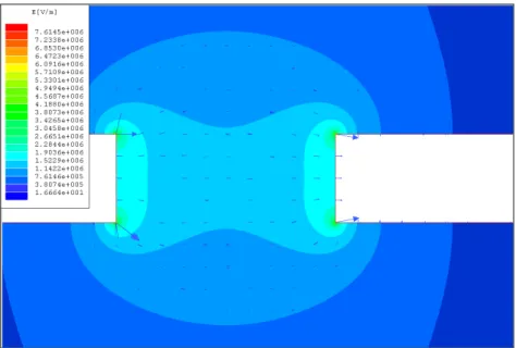
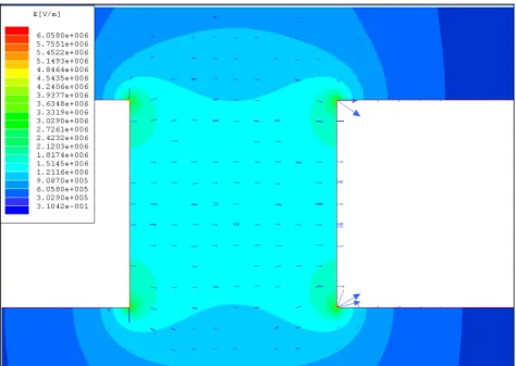
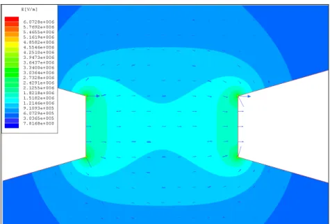
To observe the electric field and field gradients, we performed some preliminary Ansys Maxwell 2D simulations for different designs of our electrode fingers (Figure 3.1-3.6). This helped us to study which geometries possibly yield better alignment of nanowires using dielectrophoresis. In or simulations, a Vrms of 7.071 V is applied across upper electrodes of gold. The
medium is chosen to be isopropanol. The parameters of our simulation include
εgold= 6.9 εo, σgold= 4.5x10⁷ Sm-1, εipa=18.3 εo, σipa= 6x10⁻⁶ Sm-1, where εo=
8.854x10⁻¹² F/m. Figure 3.1-3.6 represent simulation results of different electrode fingers.
In our simulations, we observe that thinner fingered electrodes result in higher E-field gradient across them. For example, 2 µm thick fingers provide ~2.8 times higher field gradient compared to 5 µm thick fingers. Also, we find out that fingered electrodes are more useful in dielectrophoresis as they facilitate higher field gradient compared to the fingerless electrodes of the same thickness with a 2 µm wide ending on the edges. The electric field and the field gradient is observed to be the highest at the corners and high only at the vicinities of the edges where two electrodes are the most closest to each other as expected.
16
Figure 3.1 E-field map simulated for 2 µm x10 µm gold fingered electrodes with a gap of 5 µm.
Figure 3.2 Gradient square of the E-field simulated for 2 µm x10 µm gold fingered electrodes with a gap of 5 µm.
17
Figure 3.3 E-field map simulated for 5 µm x 10 µm gold fingered electrodes with a gap of 5 µm.
Figure 3.4 Gradient square of the E-field simulated for 5 µm x 10 µm gold fingered electrodes with a gap of 5 µm.
18
Figure 3.5 E-field map simulated for fingerless electrodes (2 µm wide on the edge) with a gap of 5µm.
Figure 3.6 Gradient square of the E-field simulated for fingerless electrodes (2µm wide on the edge) with a gap of 5 µm.
19
In our work, we fabricate arrays of microelectrodes in parallel on silicon substrates with different designs using standard microfabrication techniques including photolithography, metal deposition, liftoff, and plasma enhanced chemical vapor deposition (PECVD). On a silicon substrate, we deposit silicon oxide (SixOy) of 500 nm in thickness with a rate of 28 nm/s at 12 W at 250°C (or
sometimes silicon nitride, (SixNy) instead of silicon oxide) as the isolation layer
using PECVD to decrease the leakage current, to allow for achieving higher electric field between upper electrodes during dielectrophoretic alignment, and to reduce noise level during I-V characterizations while probing the electrodes. On the top of this dielectric layer, using photolithography, metal deposition, and liftoff, we define and pattern the first metal layer made of gold (bottom electrodes) that provides an electrical path to upper electrodes by conducting current through AC coupling. This bottom metal layer consists of 20 nm thick Ti, 100 nm thick Au, and 20 nm thick Ti. Titanium is used for adhesion layer between gold and SixNy. Subsequently, we grow an adjacent silicon nitride layer
of 200 nm at a rate of 8 nm/s at 12 W at 250°C, which serves as the dielectric layer for capacitive coupling between the lower electrodes and the upper electrodes. This dielectric layer also prevents electrical shortage of these electrodes by the metallic nanowires (NWs) during the assembly process and enables characterization of each NW one by one. Finally, we define and pattern the upper gold microelectrodes, which consists of 10 nm thick Ti and 100 nm thick Au layers on the silicon nitride layer using the same fabrication techniques as the first layer, (Figures 3.7, Figure 3.8 and Figure 3.9) [46].
20
(a) (b)
Figure 3.8 Mask design of lower and upper electrodes in (a) and (b), respectively.
Figure 3.9 Top view of optical microscopy image of two electrodes along with a zoom-in of lower electrodes.
To fabricate smooth fingers on the lower electrodes, where nanowires are aligned, we employ a bi-layer liftoff process (using liftoff resist and photoresist together) or image reversal lithography process (using on image reversal mask and negative photoresist). These significantly improve the liftoff metals. For the image reversal mask, we use AZ 5214E photoresist as the negative resist. The process starts with the spinning of the resist at 5,000 rpm, which results in a film thickness of 1.25 µm. Then, the resist is baked for 55 s at 110°C. Subsequently, the sample is exposed under UV in Karl Suss mask aligner and the figures of the electrodes are defined. The first exposure time is 15 s at 5 mW. After baking one more time for 2 min at 120°C, the second exposure lasts for 45 s at 5 mW.
For the bi-layer liftoff process, we use a direct mask. We first spin the liftoff resist (LOR) at 4000 rpm for 40 s and bake it at 170°C. For a clean liftoff, the LOR film is required to be thicker than the metal deposition thickness at least by 1.33 times [47]. Next, we spin AZ 5214E resist at 5000 rpm for 40 s and bake it at 100°C for 2 min to increase the developing time after exposing UV in the mask aligner. This allows for creating large undercut with long developing time
21
as necessary. The samples are exposed for 36 s at 5 mW. The figures defined on sample are developed using AZ 400K and the sample is subsequently washed. Then, the metal evaporation and liftoff steps follow. The gaps between our electrode fingers are designed to be either 5 or 6 µm, depending on the column in which they are located (see Figure 3.12, Figure 3.14, and Figure 3.16). The large contact pads and the paths of the lower electrodes are designed to achieve the desired capacitive coupling between top and bottom metal layers. The large contact pads are 800 µm x 800 µm and the width of the path of the lower electrodes is 60 µm. These parameters are designed to provide reasonable levels of electric field between the fingers of the upper electrodes. For that, the potential between the alignment electrodes is maximized increasing the coupling area between lower and upper electrodes when the voltage is applied to the large contact pads [48]. The choice of SixNy as the dielectric between the two
electrodes stems from its higher dielectric constant of 7.5 compared to that of SixOy (3.9), which is another factor that increases the potential between the
alignment electrodes on the chip. In Figures 3.10-3.16, scanning electron microscopy (SEM) images of the microelectrode fingers on Si/SixOy platform
are shown.
22
Figure 3.10 General top-view of one of our fabricated chips.
Figure 3.11 A 3 µm x15 µm fingered electrode with a gap of 5 µm.
23
Figure 3.13 A 5 µm x15 µm fingered electrode with a gap of 5 µm.
24
3.15 A Fingerless electrode with a gap of 5 µm.
25
Chapter 4
Nanowire synthesis
4.1 Nanowire synthesis
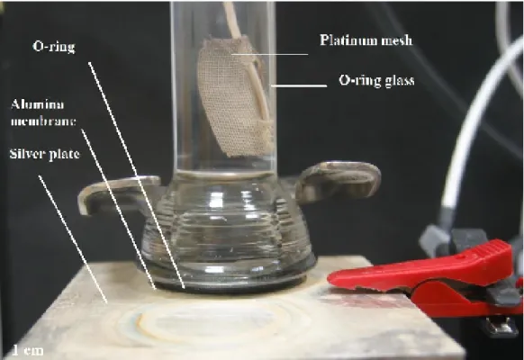
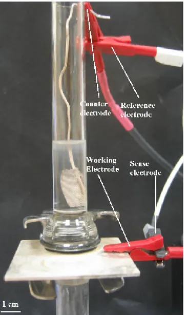
Using electrodeposition, we synthesize Au-Ag-Au segmented nanowires in porous circular membranes made of aluminum oxide (Whatman Anodisc) employed as the hard template [49]. These membranes are 21 mm in diameter and 60 µm thick with a pore size of 200 - 300 nm and a pore density of 10 9/cm2. Before electrodeposition, the back side of this aluminum oxide (alumina) membrane, where there are branched pores, is coated with 300 nm thick silver by evaporation to be used as the cathode during galvanostatic deposition. For the anode, a platinum mesh, whose area is comparable to the area of the porous membrane is used. The silver coated side of the alumina membrane is placed on the silver plate so that this side serves as the cathode. The silver plate is cleaned each time before the experiment to make sure the conduction is good during the electrodeposition, just in case it is oxidized. By using o-ring and o-ring glass on the top of the disc, we prepare our electrodeposition setup for deposition baths (Figure 4.1.1). The use of such an o-ring prevents the leakage of the gold or silver bath. The working electrode connects to the silver plate at which the desired deposition occurs. The sense electrode also is connected to the working electrode. On the other hand, the counter electrode is connected to the platinum mesh, and the reference electrode is connected to the counter. The sense electrode, which is connected to the working electrode, measures and controls the voltage between the working electrode and the reference electrode. The counter electrode, which is connected to the platinum mesh, on the other hand,
26
controls the power out put of the potentiostat (Versastat3) electrode (Figure 4.1.2). The reference electrode, which connects to the counter electrode, measures and controls the voltage between the counter electrode and the sense electrode (Figure 4.1.3).
Figure 4.1.1 Our own experimental setup for electrodeposition that includes template membrane disc, o-ring, and plates.
27
Figure 4.1.3 Our experimental setup for electrodes.
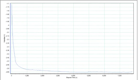
We use the method of chronopotentiometry for electrodeposition, where a fast rising current pulse is forced on the working/sense electrode and the potential of this electrode is measured against a reference electrode as a function of time. First, we deposit silver by chronopotentiometry with a current level of -1.6 mA for 1200 s from the silver bath. This makes sure that the branching portion of the membrane is clogged. The reduction of silver ions occurs for a potential range of -1.40 V and -1.70 V for -1.6 mA of current (Figure 4.1.4). Second, we start the deposition of the first gold segment using a current level of -1.6 mA for 3600 s in the gold bath. Our rate of gold deposition is 60 nm/min.
28
The reduction of gold ions occurs for a potential range of -1.70 V and -2.65 V for -1.6 mA of current (Figure 4.1.5). For subsequent Ag segment that determines the size of our gap, we employ a constant current level of -1.6 mA while varying deposition times to make Ag segments of varying lengths ranging from 20 nm to 300 nm (Figure 4.1.6). Our rate of silver deposition is 85 nm/min.
Figure 4.1.4 Potential trace during silver deposition into the branched part of the alumina disc.
Figure 4.1.5 Potential trace during gold deposition into the pores of the alumina disc for Au segments of our nanowires.
29
Figure 4.1.6 Potential trace during silver deposition into the pores of the alumina disc for Ag segments of our nanowires.
30
The views of the backside of the membrane disc before and after synthesis steps such as silver backing, gold and silver depositions are presented in Figure 4.1.7.
(a) (b)
(c) (d)
Figure 4.1.7 Backside of the membrane disc (a) before deposition, (b) after silver backing, (c) after Au deposition, (d) after Ag deposition.
31
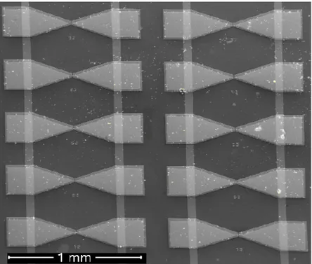
Depending on the deposition time, we produce nanowires with size controllable segments. Last, we deposit Au following Ag deposition, again applying the same current for the same deposition duration with the first Au segment. The total length of Au-Ag-Au segmented nanowire is thus made long enough to bridge the electrodes of our previously fabricated microelectrodes (Figures 4.1.8, Figure 4.1.9, and Figure 4.1.10).
32
Figure 4.1.9 SEM image of an exemplary nanowire with a short Ag segment in the middle between long Au segments at the ends (with a total nanowire length of 7.78 µm).
33
After finishing the electrodeposition, the back silver side is etched with nitric acid solution (HNO3 of 30% in concentration) and of alumina disc is dissolved
in sodium hydroxide solution (NaOH of 3 M). Nanowires remain in base solution during dissolution. Subsequently, nanowires are centrifuged three times in water at 3000 rpm for 6 min for rinsing, and three times in methanol at 3000 rpm for 6 min, and finally dispersed in methanol (Figure 4.1.11). In Figure 4.1.12, the nanowires are randomly distributed and immobilized on substrate.
Figure 4.1.11 Our nanowires suspended in methanol.
34
4.2 Nanogap variation study
We also worked on gap variation study showing that the length of Ag segment can be controlled by deposition time. The rate of the silver deposition is 85 nm/s. We synthesize Au-Ag-Au segmented nanowires that include Ag segments with lengths of 20-50-100-200-300 nm controllably (Figure 4.2.1 and Figure 4.2.2). Figure 4.2.1 shows different lengths of Ag segments (blue points). The length of the Ag segment is linearly proportional to the total charge carried to the pores of the membrane disc. As we drive constant current (I), the charge (Q) is also linearly proportional with the deposition time (t) of silver with the relation Q= I x t, which allows for controlling the lengths of Ag segments. The deviation among the lengths of Ag segments stems from not being able to drive perfectly same current into the pores of the alumina from different parts of the disc, and this deviation increases proportionally with deposition time (Figure 4.2.1 (black lines)). When Ag segment is selectively chemically etched, we form a nanogap with a size equal to the size of our Ag segment.
Figure 4.2.1 Gap length vs. charge. (Blue points represent the lengths of Ag segments, and black lines represent the standard deviation among Ag segment lengths.)
35
Figure 4.2.2 Example of Au-Ag-Au segmented nanowires with varied Ag segment lengths of 300 nm, 200 nm, 100 nm, 50 nm, and 20 nm in (a), (b), (c), (d), and (e), respectively.
36
For gold nanoparticle synthesis, 1mM Hydrogentetrachloroaurate (III) trihydrate (HAuCl4.3H2O) aqueous solution is prepared (~0.08g HAuCl4 in 200
ml DI water). This solution is heated to 300°C. 44 mM sodium citrate dehydrate solution (0.26g in 20 ml DI water) is dropped into HAuCl4.3H2O solution while
boiling. After becoming dark, the color of the solution starts to turn into red, showing that gold nanoparticles are synthesized after the reaction (Figure 4.2.3) [50]. These gold nanoparticles are used in our dielectrophoresis experiments, too. Absorbance spectrum of gold nanoparticles is seen in Figure 4.2.4.
Figure 4.2.3 Our gold nanoparticles in water.
37
CHAPTER 5
Our dielectrophoresis experiments
5.1 Dielectrophoretic alignment of our nanowires
Using dielectrophoresis, we align our nanowires on the previously fabricated microelectrode arrays with a purpose of single nanowire alignment across each of the electrode pairs in the array. We drop 25-30 µl of the methanol solution containing 7.2 µm long Au-Ag-Au segmented nanowires on our electrode microchip when the signal generator is turned on. We apply an AC bias across the primary pads of our microchip on the corners. Applying the signal, the movement of nanowires is monitored in real time through the optical microscope in the probe station. The dropping step is repeated 2-3 times in order to allow the nanowires to flow in the medium without getting stuck on the chip base and to get manipulated by dielectrophoretic force across the electrode fingers. Multiple dropping also increases the nanowire number in the medium. For our devices on Si/SixOy substrate, we achieve alignments by applying a
sinusoidal wave with Vpp =50 V across our primary pads for 30-45 s at 10 kHz
by observing the chip under the microscope. Nanowires polarize in the applied AC field. As they are more polarizable than the dielectric medium, they align moving towards the electrode fingers as a result of the dielectrophoretic force, which is maximized at the high field gradients across the fingers.
38
Effect of frequency:
The required modulation frequency applied for manipulating nanowires depends on the dielectric constants and conductivities of the medium and nanowires. The resulting dielectrophoretic force is strong for Au-Ag-Au nanowires in methanol at 10 kHz. Below 500 Hz, weaker manipulation of nanowires is observed. For higher frequencies, higher field is needed to achieve the same level of dielectrophoretic force, as the induced charges cannot follow the change of polarization with the applied electrical field [24].
For water soluble particles, we apply dielectrophoresis in water at a different frequency of 1MHz, since the dielectric property and the conductivity of the medium substantially changes compared to methanol.
Effect of voltage (electric field magnitude):
A certain necessary amount of potential difference needs to be applied on main pads to achieve required dielectrophoretic force on nanowires. For Vpp<50 V,
the resulting dielectrophoretic force is not strong enough to form bridges between microelectrodes by aligning nanowires. For Vpp>50 V, undesired
multiple nanowire alignments start on our microelectrode chips. Therefore, we find the optimal Vpp=50 V in our case.
Effect of nanowire concentration:
Another parameter is the nanowire concentration. Increasing nanowire concentration also increases the number of single alignments, but this comes at the cost of increased multiple alignments at the same time. Therefore, we use a reasonable nanowire concentration of 2.5x10⁷ ml-1, which achieves high yield alignments up to % 40.
Effect of viscosity:
The viscosity of the host medium is also an effective parameter for alignment. Less viscous medium is more useful to manipulate suspending nanowires [24]. As we cannot specifically analyze the effect of viscosity in liquids solely as they
39
also have different dielectric constants, we observe the effects of these two properties together. We observe that methanol, which has a viscosity of 0.584 cP at 25°C and a dielectric constant of 32.6, increases the yield of the alignment compared to isopropanol, which has a viscosity of 1.96 cP at 25°C and a dielectric constant of 20.18. After the field is applied, before the methanol dries over the chip, we clean the chip gently by nitrogen gun to get rid of the un-aligned nanowires.
5.2 Clamping of the nanowires and I-V
characterization
Following the nanowire alignment, 20 nm Ti / 300 nm Au clamps are patterned on the two sides of the microelectrode arrays to anchor the nanowires on the fingers of electrodes (Figure 5.2.1, Figure 5.2.2, Figure 5.2.3, and Figure 5.2.4). In addition, clamps facilitate a better contact between the electrodes and nanowires. At this stage, we obtain I-V characteristics of nanowires (by applying a compliance of 100 nA to prevent nanowires potentially from heating and melting with large current densities). A SEM image of the aligned and clamped nanowire is depicted in Figure 5.2.1, along with its I-V characteristics in the inset, verifying electrical conductance through the nanowire when the two ends of the microelectrodes are probed.
Figure 5.2.1 SEM image of the aligned and clamped Au-Ag-Au segmented nanowire, and its I-V plot in the inset.
40
41
Figure 5.2.3 SEM image of the nanowire aligned dielectrophoretically, before clamping.
42
5.3 Nanogap formation
After aligning Au-Ag-Au nanowires, Ag segments of nanowires are removed by post-baking process at 200°C for 75 min [51] and/or chemically etching Ag with dilute nitric acid (HNO3)solution. This allows for the two ends
of the nanowire to be automatically and precisely aligned (Figure 5.3.1).
(a)
(b)
Figure 5.3.1 SEM images of the nanowire before and after nanogap formation in (a) and in (b), respectively.
43
Difficulties in nanogap formation are sometimes encountered due to the high tendency of Au deposition at the walls of alumina pores, forming a meniscus at the frontline of deposition. This negatively affects the morphology of the nanowires, resulting in a curved profile across the radial dimension. In addition to chemical etching, baking process is also employed to remove Ag segments, and which also helps smoothening of our nanogaps [51]. Thermal baking of nanowires enables us to form narrower, uniform gaps, and also strengthens the electrical contacts on the gold ends of nanowires made with the measurement electrodes of the microelectrode arrays. In Figure 5.3.2, the nanowire with its nanogap formed by selective silver etching is pictured. In this case, we observe clear open circuit behavior in its I-V measurements, confirming that nanogap formation was successful.
Figure 5.3.2 SEM image of the nanowire after gap formation in the middle, and its I-V plot in the inset.
44
5.4 Nanoparticle capture
We achieve high electric fields across the etched gap between Au segments of the nanowire. Nanoparticles in aqueous solution are dropped on the chip where they are initially randomly distributed. Applying a sinusoidal wave with Vpp of 10 V at 1 MHz across primary pads for 45 s, we apply electric field
between nanogaps formed in the middle of nanowires. Polarized gold nanoparticles are then trapped in these nanogaps where the field gradient and resulting dielectrophoretic force is high (Figure 5.4.1).
Figure 5.4.1 SEM image of a nanoparticle trapped in nanogap dielectrophoretically.
Finally, after capturing nanoparticles in the gap, we observe strong electrical conduction again across the electrodes (Figure 5.4.2).
45
Our approach combines the benefits of using segmented nanowires and their alignment using dielectrophoresis. One of the key benefits in this combined approach is that the aligned nanowires automatically provide electrical contacts to the captured nanoparticles to allow for probing and characterizing these nanoparticles at the nanoscale. Also, since nanogaps are formed with the selective removal of the mid section of nanowires, the two ends of the nanowires are automatically self-aligned. In the process, before the removal of mid Ag section, we observe electrical conductance through the continuous Au-Ag-Au nanowire by probing the two connected microelectrodes (in the inset of Figure 5.4.3(b)). However, after the removal of mid section, we observe the open circuit behavior, confirming the formation of a gap (in the inset of Figure 5.4.3(c)). Finally, after capturing nanoparticles in the gap, we observe strong electrical conduction again across the electrodes. This indicates that our nanowire arrays with size controllable nanogaps provide a nanoscale device platform convenient for nanoparticle capturing and electrical characterization (Figure 5.4.3(d)).
46
Figure 5.4.3 SEM images of (a) microelectrode fingers before nanowire alignment (along with their I-V showing open circuit in the inset), (b) aligned Au-Ag-Au segmented nanowire by using DEP and clamps (along with its I-V showing electrical conduction in the inset), (c) nanowire after gap formation in the middle (along with its I-V showing open circuit again in the inset), and finally (d) nanoparticles captured in the size controllable nanogap by using DEP (along with I-V showing electrical conduction in the inset).
47
Chapter 6
Conclusion
In our thesis research work, we proposed and demonstrated constructing an on-chip nanowire device for manipulating, capturing, and electrical characterization of nanoparticles. For this purpose, we synthesized Au-Ag-Au segmented nanowires and dielectrophoretically aligned these nanowires on our microfabricated array of electrodes. After the nanowires were aligned, we selectively removed the mid Ag segment, obtaining self aligned two Au nanowire segments with a nanogap between them. Also making a systematic study of the gap size variation, we opened nanogaps of different sizes, which can be used for different characterizations and different applications, showing the feasibility of managing gap formation controllably.
In each step of integration, we made I-V measurements and SEM imaging to show our proof-of-concept demonstration of the nanowire device integrated with microelectrodes. First, we observed an open circuit between the empty microelectrode fingers before nanowire alignment. Second, a short circuit was observed when we aligned the Au-Ag-Au segmented nanowires on the microelectrodes. Third, an open circuit was observed again between the Au ends of the nanowires when we formed nanogaps by removing the middle Ag segments. Finally, a short circuit was observed again between the Au ends of the nanowires after capturing of gold nanoparticles in the nanogaps. This shows that we electrically contacted the nanoparticles trapped in nanogaps to the nanowires and the nanowires to the microelectrodes.
Our approach allows for full integration from nanoparticles to nanowires to microelectrodes to macroprobes on a single chip enabling the electrical characterization of various nanoparticles.
48
BIBLIOGRAPHY
[1] M. P. Hughes, “AC electrokinetics: applications for nanotechnology,” Nanotechnology 11, 124-132 (2000).
[2] R. Pethig, Y. Huang, X. B. Wang, and J. P. H. Burt, “Positive and negative dielectrophoretic collection of colloidal particles using interdigitated castellated microelectrodes,” J. Phys. D: Appl. Phys. 24, 881-888 (1992).
[3] X. B. Wang, Y. Huang, P. R. C. Gascoyne, and F. F. Becker, “Dielectrophoretic manipulation of particles,” IEEE Transactions on industry applications 33, 660-669 (1997).
[4] N. G. Green, and H. Morgan, X “Dielectrophoretic separation of nano-particles,” J. Phys. D: Appl. Phys. 30, L41-44 (1997).
[5] T. B. Jones, “Electromechanics of particles,” Cambridge: Cambridge University Press (1995).
[6] W. M. Arnold, and U. Zimmermann, “Rotating-field-induced rotation and measurement of the membrane capacitance of single mesophyll cells of Avena Sativa,” Z. Naturforsch. C 37, 908-915 (1982).
[7] X. B. Wang, Y. Huang Y, F. F. Becker, and P. R. C. Gascoyne, “A unified theory of dielectrophoresis and travelling wave dielectrophoresis,” J. Phys. D: Appl. Phys. 27, 1571-1574 (1994).
[8] H. A. Pohl “Dielectrophoresis,” Cambridge: Cambridge University Press (1978).
49
[9] L. Zheng, S. Li, J. P. Brody, and P. J. Burke, “Manipulating nanoparticles in solution with electrically contacted nanotubes using dielectrophoresis,” Langmuir 20, 8612-8619 (2004).
[10] M. Washizu, O. Kurosawa, I. Arai, S. Suzuki, and N. Shimamato, “Applications of electrostatic stretch and positioning of DNA,” IEEE Trans. Ind. Appl. 31, 447-456 (1994).
[11] T. Müller , A. Gerardino , T. Scnelle , S. G. Shirley, F. Bordoni, G. DeGasperis, R. Leoni, and, G. Fuhr, “Trapping of micrometer and sub-micrometer particles by high frequency electric fields and hydrodynamic forces,” J. Phys. D: Appl. Phys. 29, 340-349 (1996).
[12] N. G. Green and H. Morgan, C. D. W. Wilkinson and J.J. Milner, “Dielectrophoresis of virus particles,” Proc. St. Andrews Meeting of the Society for Experimental Biology (St Andrews, UK), 77 (1994).
[13] N. G. Green, H. Morgan, and J. J. Milner, “Manipulation and trapping of sub-micron bio-particles using dielectrophoresis,” J. Biochem. Biophys. Methods 35, 89-102 (1997).
[14] O. D. Velev, and E. W. Kaler, “In situ assembly of colloidal particles into miniaturized biosensors,” Langmuir 15, 3693-3698 (1999).
[15] P. R. C. Gascoyne, X. B. Wang, Y. Huang, and F. F. Becker, “Dielectrophoretic separation of cancer cells from blood,” IEEE Transactions on industry applications 33, 670-678 (1997).
[16] J. Yang, Y. Huang, X. B. Wang, F. F. Becker, and P. R. C. Gascoyne, “Differential analysis of human leukocytes by dielectrophoretic field-flow- fractionation,” Biophysical Journal 78, 2680–2689 (2000).
50
[17] M. P. Hughes, and H. Morgan, “Dielectrophoretic trapping of single sub-micron-scale bioparticles,” J. Phys. D: Appl. Phys. 31, 2205-2210 (1998).
[18] S. Tuukkanen, A. Kuzyk, J. J. Toppari, H. Hakkinen, V. P Hytönen, E. Niskanen, M. Rinkiö, and P. Törma, “Trapping of 27 bp–8 kbp DNA and immobilization of thiol-modified DNA using dielectrophoresis,” Nanotechnology 18, 295204 (2007).
[19] K. Hoshino, K. Yamada, K. Matsumoto, and I. Shimoyama, “Creating a nano-sized light source by electrostatic trapping of nanoparticles in a nanogap,” J. Micromech Microeng. 16, 1285-1289 (2006).
[20] R. Zhou, H. C. Chang, V. Protasenko, M. Kuno, A. K. Singh, D. Jena, and H. (G.) Jing, “CdSe nanowires with illumination-enhanced conductivity: induced dipoles, dielectrophoretic assembly, and field-sensitive emission,” J. Appl. Phys. 101, 073704 (2007).
[21] S. Y. Lee, T. H. Kim, D. I. Suh, J. E. Park, J. H. Kim, C. J. Youn, B. K. Ahn, S. K. Lee, “An electrical characterization of a hetero-junction nanowire (NW) PN diode (n-GaN NW/p-Si) formed by dielectrophoresis alignment,” Physica E 36, 194-198 (2007).
[22] S. H. Hong, M. G. Kang, H. Y. Cha, M. H. Son, J. S. Hwang, H. J. Lee, S. H. Sull, S. W. Hwang, D. Whang, and D. Ahn, “Fabrication of one-dimensional devices by a combination of AC dielectrophoresis and electrochemical deposition,” Nanotechnology 19, 105305 (2008).
[23] J. J. Boote, and S. D. Evans, “Dielectrophoretic manipulation and electrical characterization of gold nanowires,” Nanotechnology 16, 1500– 1505 (2005).
51
[24] K. H. Bhatt, and O. D. Velev, “Control and modeling of the dielectrophoretic assembly of on-chip nanoparticle wires,” Langmuir 20, (2004).
[25] K. D. Hermanson, S. O. Lumsdon, J. P. Williams, E. W. Kaler, and O. D. Velev, “Dielectrophoretic assembly of electrically suspensions functional microwires from nanoparticle,” Science 294, 1082 (2001).
[26] X. Xiong, A. Busnaina, S. Selvarasah, S. Somu, M. Wei, J. Mead, C. L. Chen, J. Aceros, P. Makaram, and M. R. Dokmeci, “Directed assembly of gold nanoparticle nanowires and networks for nanodevices,” Appl. Phys Lett. 91, 063101 (2007).
[27] S. J. Papadakis, Z. Gu, and D. H. Gracias, “Dielectrophoretic assembly of reversible and irreversible metal nanowire networks and vertically aligned arrays”, Appl. Phys. Lett. 88, 233118 (2006).
[28] P. J. Hesketh, M. A. Gallivan, S. Kumar, C. J. Erdy, and Z. L. Wang, “The applications of dielectrophoresis to nanowire sorting and assembly for sensors,” Proceedings of the 2005 IEEE International Symposium, Mediterrean Conference on Control and Automation, 153-158 (2005).
[29] Y. Dan, Y. Cao, T. E. Mallouk, A. T. Johnson, and S. Evoy, “Dielectrophoretically assembled polymer nanowires for gas sensing,” Sensors and Actuators B 125, 55-59 (2007).
[30] L. Shang, T. L. Clare1, M. A. Eriksson, M. S. Marcus, K. M. Metz, and R. J. Hamers, “Electrical characterization of nanowire bridges incorporating biomolecular recognition elements,” Nanotechnology 16, 2846–2851 (2005).
![Figure 2.1.1.1 Schematic diagram of the net force acting on a polarizable Particle due to the interaction of induced charges and local electric field [1]](https://thumb-eu.123doks.com/thumbv2/9libnet/5745840.115811/16.892.267.691.182.461/figure-schematic-diagram-polarizable-particle-interaction-induced-electric.webp)