PHYSICAL REVIEW
8
VOLUME 47, NUMBER 24 15JUNE 1993-IIAbsence
of
metallicity
in
Cs-GaAs(110):
A
Hubbard-model
study
Z.
Gedik andS.
CiraciDepartment
of
Physics, Bilkent University, Bi!kent 06533,Ankara, Turkey InderP.
BatraIBMResearch Division, Almaden Research Center, 650Harry Road, San Jose, California 95120-6099
(Received 3 February 1992)
Using an approximate solution ofthe Hubbard-model Hamiltonian, we are able to establish that the
Cs-GaAs(110) system becomes a Mott insulator at submonolayer Cs coverages. We also provide a con-sistent interpretation ofelectron-energy-loss and scanning-tunneling-spectroscopies data. The correla-tion effects are important forthis system with an estimated correlation energy of 0.4 eV.
The adsorption
of
alkali-metal (AM) overlayers on semiconductor surfaces has attracted considerable in-terest recently. ' The fillingof
the active dangling-bond surface states by the weakly bound valence electronof
the adsorbed AM atoms underlie several properties, such as bonding, surface reconstruction, metallization, and collective excitations. The current issues subject to active investigation are the characterof
the bonding and surface metallization, and the adsorption site at various stagesof
AM coverage. Numerous observations are consistent with the fact that the properties exhibit significant varia-tions depending on the rangeof
coverage. Total-energy calculations ' show that potassium can be adsorbed ontoat least four different sites on the
Si(001)-(2X
1)surface, which areof
comparable binding energy, implying that the bonds formed with AM atoms are nondirectional.Electronic structure and charge-density analysis
of
several AM-covered semiconductor surfaces indicated that the weakly bound valence-electronof
the adsorbed atom is donated to the empty dangling-bond surface state. In some cases, the dispersion and the charge dis-tributionof
this band do not change significantly uponfilling with alkali adsorption. Having no unambiguous
way to measure the charge transfer, this has been taken as evidence
of
a strongly ionic bondingof
the AM atom with semiconductors. Previous assertions that the bond should be covalent are now reconciled with apartly ionic picture, even for an estimated charge transferof
0.
6 elec-trons.Earlier, in the analysis
of
the stabilityof
reconstruction upon the AM adsorption, we pointed out the strong electron-correlation effect in the fillingof
the Aatsurface-state band. These arguments appear to be valid for the electronic structure
of
the GaAs(110) surface at submonolayer Cs coverage:It
is established that in the clean GaAs(110) surface the surface atoms relax; while theGa
atoms are lowered relative to their ideal positions, the As atoms are raised. The buckling is, however, re-duced upon absorptionof
an alkali atom. Previous electron-structure calculations based on the local-density approximation (LDA) yielded a finite densityof
states (DOS) at the Fermi level in the band gap for the half monolayer(8=0.
5) as well as for the monolayer(8=1)
coverage
of
AM."
The difference charge-density (i.e.
,charge density with AM minus that without AM) analysis revealed that the charge due
to
the adsorbed AM has a dangling-bond orbital character and is strongly lo-calized at the surface Ga atoms."
However, the data ob-tained from scanning tunneling microscopy (STM),' scanning tunneling spectroscopy (STS),' photoemission electron spectroscopy, ''
and electron-energy-loss spec-troscopy(EELS)
(Ref. 16) provided evidence that the Cs-covered GaAs(110) surface is insulating for8(1.
Ap-parently, these experimental results are at variance with the standard energy band-structure calculations predict-ing metallicDOS.
Earlier, the chain structure revealed by STM at low
coverage was identified as the one dimensional
(1D),
zig-zag chainof
adsorbed Cs atoms. ' Such a chain involves a localc(2X2)
surface structure with8=0.
5 coverage. An extended areaof
adjacent zigzag chains leads to a hexagonal-like structureof
Csatoms with the Bravais lat-tice vectorsof
~R&~=6.
9 A and ~R2~=7.
9A.
Thecover-age
0=1
is supposed to leadto
a rectangular structure having the unit cellof
the GaAs(110) surface. ' We name this structure as the compressed phaseor
rectangu-lar structure. Recent current-voltage measurements (STS) (Ref. 13) over various Cs structures on GaAs(110) clearly show that the band gapof
the clean surface is1.
4 eV. However, first itdecreases to1.
1eV for 1D structureat
0=0.
1,later to0.
6eV for 2D structure at0=0.
6.
Fi-nally, at the onset
of 3D
overlayer for8
~
1,the band gap diminishes, leading to a conducting state. In compliance with the earlier observations, the 1D structure is made from zigzag chains, which become wider upon the forma-tionof
adjacent chains at increased0,
whereas, recent STM imagesof
2D phase are identified as five-atom po-lygons with a localc(4X4)
structure. ' The local elec-tronic structureof
Cs overlayer revealed by STM and STS is in agreement with the interpretationof
EELS.
'For 0
—
+0.5the band gap narrows in theEELS
spectrum. Two loss peaks (at0.
42 and1.
04eV) originating from lo-calized excitations appear only when8&0.
5.
Near the saturation coverage at room temperature(8=0.
9)
a new loss peak appears at1.
14 eV. Additional Cs coverage, which takes place only at low temperature, shifts thisI6392 Z.QEDIK, S.CIRACI, AND INDER P.BATRA 47
U=e
Jd
rdr'
/r
—
r'/ (2)In the presence
of
local vibrational excitations, there may arise a negative-U term that renorrnalizes the Coulomb repulsion. However, in our system, owing to theinsulat-ing nature
of
the metal layer, we assume that electron-phonon interactions are not important. Although its ex-act solution is not known, there has been great progressin understanding the nature
of
the Hubbard model for the 2D square lattice, due to the widely accepted viewpeak to the plasmon energy
of
bulk Cs. Concomitantly, the band gap is filled by a continuumof
excitations.The evolution
of
the electronic structure with coverage0
~
8
~
1isidentified by the transition from 1D-2D (Mott) (Ref. 17) insulatorto
3Dmetal.It
isargued that the elec-tron densityof
the overlayer is low, and the electronic structure can be described by many electron models in-voking on-site Coulomb energy U. ' Becauseof
U, the densityof
states in local(1D
or 2D) AM structures on the GaAs(110) surface splits to prevent double occupancy at agiven site.There are various phenomena that give rise to the metal-insulator transition. '
For
example, a change incrystal structure may create agap in energy spectrum. In Cs-covered GaAs(110), a local change in the periodic structure isnot compatible with such a transition. More complicated transitions are also possible, such as those associated with Neel ordering or exciton formation. The latter is not possible for a metal-covered semiconductor surface since it requires long-lived excitons.
It
appears that the electron-electron correlation is the likely sourceof
observed transition.It
should be noted that the nearest-neighbor distanceof
the9=0.
5 structure (6.9A)
is significantly larger than that
of
bulk Cs, which isknown to be close to the Mott metal-insulator transi-tion.' In this study we investigate the effect
of
electron-electron correlation in the Cs-adsorbed GaAs(110) sur-face by using the 2D Hubbard model. ' The electronic structure derived therefrom is used to interpret STSandEELS
data.When Coulomb interaction
of
electrons is introduced,we have to add to the standard Hamiltonian, terms
in-volving four states. Those are two incoming states that interact via electrostatic force and two outgoing states into which the initial electrons are scattered. By
express-ing the Hamiltonian in terms
of
localized orbitals (such as Wannier orbitals P;), one can see that the interaction terms having the same four states have the largest magni-tude. Thus, all the interaction terms involving different sites can be neglected. This leads to the Hubbard model with the Hamiltonian'H=g
t; c; c+
—
Ugn; n;.
. (1)l,J,CT
1J ICT JC7
l,O
where c; is the creation operator for an electron
of
spino.at site
i,
n;=c;
c; isthe number operator, t,. is the transfer integral(P,
~H~PJ.)
from sitej
to site i, and Uisthe Coulomb repulsion energy between two electrons on the same site, which is given by
that it describes the physics
of
high-temperature oxide superconductors.For
high-T, materials, it has been pro-posed thatt/U (t
being the largest t, , "i.e.
,nearest-neighbor hopping, and all the other r; 's are neglected)
ra-tio may be rather small and therefore the hopping term can be treated perturbatively. In this case, using degen-erate perturbation theory, ' it is possible toshow that the model reduces to the so-called t
—
J
model, which con-tains termsof
the form—
JS;
S.
Here, S, is the spin operator for sitei,
andJ
isthe exchange integral between sites i andj,
and it is given byJ=
4t /—U. In the Cs/GaAs(110) system, thet/U
ratio is small; it may beeven smaller than that for high-T, compounds. There-fore, all the discussions related to the 2D t
—
J
model may be relevant for the Cs/GaAs(110) system also.For
our purposes it isenough to know how the correlation effects change the DOSof
the system. Here, by asite we mean the localized superorbital formed from the orbitalsof
Cs and thoseaf
the surface atom towhich Csisbound.An appropriate solution
of
the energy spectrumof Eq.
(1),which reduces to localized orbitals or Bloch states at the proper limits, is provided by the Green-function tech-nique. 'For
the sakeof
simplicity, we confine ourselvesto
the solution at0
K
and we assume that the system isnonmagnetic, thus
(n;
)
=n
=
—,'.
The last equalityfol-lows from the fact that each Cs atom donates one elec-tron to the system. Under those conditions, the density
of
statesp(E)
in the presenceof
the Coulomb repulsion is given by 1 12p(E)
=
—
g
5E
I
—
—
—
e(k)
NE
—
I
q (3)where
I
=
U/2 ande(k)
is the band structureof
thesys-tem in the absence
of
the correlation effect, that is, whenU
=
0.
We have chosen the energy scale so thatgi,
e(k)
=0.
Crystal momentum and also band structure are defined for regions that are covered with Cs and show a local 2D periodic structure. This assumption is based on the STM data. Again for simplicity, we can treat thesystem asa hexagonal orrectangular lattice for
0=0.
5or0=1,
respectively. Furthermore, for the latter structure the first- and the second-nearest-neighbor transfer in-tegrals are assumed to be equal as in a square lattice.If
we know
pb(E)
corresponding to a band structuree(k),
we can find
p(E)
by using the composite functionp(E)=pbtf (E)],
wheref
(E)=E
I
—
(I~/E
I).
For-
—
example, for the 2D square lattice (which represents the0=
1structure), pb is given by a complete elliptic integralof
the first kind.If
U=0,
f
(E)
=E
and hencep(E)=pb(E).
On the other hand, forU)
0
independent particle approximation fails, because energyof
an elec-tron at a certain site depends upon whether or not this site isalready occupied. This repulsive interaction causes the DOS to be separated into two parts, a filled onep,
& and an empty onep,
„'
the peak-to-peak energy separa-tion between them is 6=
U. The band gap isb
=+16t +
U 4t, which is smaller than—
5.
Note thatthe gap equation is the same for all structures as long as their bandwidths are equal.
For
the hexagonal structure47 ABSENCE OFMETALLICITY IN Cs-GaAs(110):
A.
.
.
16393 corresponding to0=0.
5, the peak-to-peak energyspac-ing between
p,
f
andp,
,
becomeso=+16t
+
U . Since there is no well-defined and homogeneous crystal struc-tureof
adsorbate between0=0.
5and0=
1,it isnot clear what the DOSlooks like.It
has been proposed that as Cs coverage increases from half-monolayer coverage, the0.
5phase (having hexagonal structure) gradually changes into the
8=1
phase [having rectangular structure with the lattice parametersof
the ideal GaAs(110) surfacej. ' This means that for0&1
the regionsof
the0=0.
5 and0=1
phases coexist, but the extentof
the0=1
phase in-creases as8~1.
In viewof
this model it isexpected that the DOS curve will follow a rather smooth transition from hexagonal to square lattice type. Apparently, the work by Whitman etal.
' points to a different evolutionof
the adsorbate structure as0~1.
Since there is always one electron per site for both phases
(8=0.
5 and8=1),
the lower partof
the DOS(p,
f
) is always filled and therefore the system isinsulat-ing as long as
p,
f
andp,
,
are detached. As4t/U
in-creasesp,
f
andp,
,
approach each other, eventually they touch when4t/U
=
1,EF
passing through the pointof
contact. However, our approximate solution (the so-called Hubbard-I approxiination) which is valid for t«
U, breaks down during this transition. An improved method (Hubbard-III) (Ref. 20) predicts that the gap be-tween the two piecesof
the DOS vanishes when r/U
be-comes sufficiently large. Further increaseof
4t/U
ratio causesp,
f
andp,
,
to merge into a single DOS with an increased density atEF.
Therefore, the effectof
Coulomb repulsion Uis to suppress the DOS atEF
and to open a gap between the filled and empty states,if
itislarge com-pared tot.
However,if
U is small in comparison to the bandwidth, the DOSisonly slightly modified.The evolution
of
the DOS in the band gapof
the GaAs(110) surface can be related to the coverageof
Cs. Regarding the adsorbate structure for0
&0.
5,we consid-er two possibilities. According tothe first one, zigzag Cs atoms form islands, which yields a local hexagonal struc-ture. The bandwidthof
this structure (at U=0)
can be obtained from the self-consistent pseudopotential calcula-tions usingLDA.
In the past, the electronic structureof
Na adsorbed on the GaAs(110) surface was studied as a prototype system. The conclusions drawn thereof were extrapolated to other alkali atoms adsorbed on the same surface. Since mostof
the available pseudopotentials for Cs atoms are not suitable for an accurate descriptionof
the electronic structure, the valueof
t for Cs adsorbed on GaAs(110)is estimated by calculating the ratio(4)
where HID denotes the Hamiltonian in Eq. (1) without the U term. The orbitals
%c,
)
and ~%N,)
stand for thelocalized states in Eq. (1)formed between substrate and adsorbate atoms (Cs and Na, respectively). The prime corresponds to the nearest-neighbor orbital. Here, we
have two limiting cases. In the first one there is no charge transfer from the alkali atom to the surface and therefore the localized states are simply the 6s and 4s
or-I I I I I I I I I I I I I I I I I I $A I E=1.45eV Energy
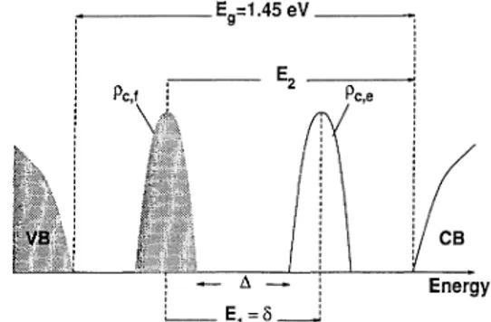
FIG.
1. Schematic description ofthe density ofstates in the band gap and the transitions therefrom. p,,
and p,f
denote the density ofstates, and E& and E2 are the transition energies.bitals
of
Csand Na, respectively. Byusing the valueof t
for the Na-GaAs(110) system" (which is=0.
04 eV) and the atomic orbitals obtained from the Herman-Skillman tables, we calculateg
=2.
6 within the Hiickel approxima-tion and hence t=0.
1 eV for the Cs-GaAs(110) system. Using the estimateof
U=
l.
5+0.
3 eV (Ref. 11)we obtaint/U
=0.
06.
In the second limit, there iscomplete charge transfer from the adsorbate to the surface states. Conse-quently, the localized states correspond to dangling bondsof Ga
character. Thus, the hopping integral is al-most independentof
the adsorbate and hence g=
1 for which t/U
=0
03.
Ac.cordingly, in both cases, the Hubbard-I approximation, which is valid as long ast/U
is sufficiently small, predicts an insulating phase. Fur-thermore, based on the above discussion one finds6
=
1.5eV and
6=1.
5 eV. Assuming thatp,
f
is0.
4 eV above the maximumof
the valence band, the present modelpro-jects
a nonmetallic state for0
+ 0.
5, but fails to explain the band-gap narrowing with increasing Cs coverage for0
&0.
5.
According tothe second possibility the structureof
the adsorbate is coverage dependent. ' At very low coverage, individual chainsof
Cshave an insulating char-acter with a local band gapof 1.
1 eV.' The filled band can split owing to the electron correlation. The empty partof
each filled band is expected to overlap with the conduction-band continua. Upon increasing coverage, a third rowof
Cs atoms is added to the zigzag structure. This increases the widthof
the filled state, and hence reduces the band gap.The 2D structure, which occurs at
0-0.
6,is different from thet9=0.
5 phase having hexagonal structure. TheEELS
peak occurring atE, =0.
42 andE2=1.
04 eV for0)
0.
5are in compliance with the compressed phase' or0=1
phase in registry with the rectangular surface unit cellof
GaAs(110) surface.For
the compressed phase, U is smaller than that in the0
=
0.
5 phase since the nearest-neighbor distanceof
the adsorbates in the formeris reduced. In view
of
the above theory, theEELS
peaksE,
and E2 are associated with the transitionsp,
f
—
+p,,
andp,
f
—
+GaAs conduction-band, respectively. This im-plies thatp,
f
lies-0.
4 eV above the maximumof
the valence band, and6=U=0.
4 eV for the rectangular structure. Figure 1 presents a schematic representation16394 Z.GEDIK, S.CIRACI, AND INDER P.BATRA 47
of
these transitions.Very recently, STM data on K-covered GaAs(110) and InSb(110) and Cs-InSb(110) systems exhibited nonmetal-lic behavior similar to that
of
the Cs-covered GaAs(110) discussed above. By using tunnelingI-V
curves, Jeon etal.
also observed the absenceof
metallicity for the Na-induced Si(111)-(3X1)
surface with —', Na coverage, which has unpaired electrons in the unit cell. These findings bring about a new aspectof
alkali-metal-covered semiconductor surfaces having unpaired electrons. That is the Mott insulating behavior and support the modelgiven above.
In conclusion, using the Hubbard model we investigat-ed the electronic structure
of
the Cs-covered GaAs(110) surface at submonolayer coverage. The electron hopping and electron repulsion energy estimated from self-consistent field calculation indicate that the correlation efFects are important and cause the metallic densityof
states in the band gap to split. As a result the system be-comes a Mott-Hubbard insulator with the absent densityof
states at the Fermi level up to monolayer coverageof
Cs. Using an approximate solution
of
the model, we pro-vided an interpretationof
electron-energy-loss andscan-ning tunneling spectroscopies.
H. Tochiara, Surf. Sci. 126,523(1983);T.Aruga, H. Tochiara,
and
Y.
Murata, Phys. Rev.Lett. 53,372(1984).S.Ciraci and
I.
P.Batra, Phys. Rev. Lett. 56,877 (1986);ibid.58, 1982(1987);ibid. 60, 547 (1988);Phys. Rev. B 37, 2995 (1988).
I.
P.Batra, Phys. Rev.B43,12322(1991).T.
Kendelewicz, P.Soukiassian,R.
S.List,J.
C.Woicik, P. Pi-anetta,I.
Lindau, and W.E.
Spicer, Phys. Rev. B37, 7115 (1988).5E.M. Oellig,
E.
G.Michel, M.C.Asensio,R.
Miranda,J.
C. Duran, A. Munoz, andF.
Flores, Europhys. Lett. 5, 727(1988).
6Metallization and Metal Semicond-uctor Interfaces, edited by
I.
P.Batra (Plenum, New York, 1989).
7I.P.Batra,
E.
Tekman, and S. Ciraci, Prog. Surf. Sci. 36,289 (1991).I.
P.Batra and S. Ciraci, Phys. Rev.B37,8432{1988). C.Y.
Fong, L.H.Yang, andI.
P.Batra, Phys. Rev.B40, 6120(1989).
J.
Ortega andF.
Flores, Phys. Rev.Lett. 63, 2500 (1989).J.
Hebenstreit, M. Heinemann, and M. SchefBer, Phys. Rev. Lett. 67,1031(1991).~P.N. First, R.A.Dragoset,
J.
A. Stroscio,R.
J.
Celotta, andR.
Feenstra,J.
Vac.Sci.Technol. 7, 2868(1989).L.
J.
Whitman,J.
A. Stroscio,R.
A. Dragoset, andR.
J.
Celotta, Phys. Rev. Lett. 66, 1338(1991).~K. O.Magnusson and
B.
Reihl, Phys. Rev.B40, 7814 (1989).T.
M.Wong, N.J.
DiNardo,D.
Heskett, and E.W.Plummer,Phys. Rev. B41,12342(1990).
N.
J.
DiNardo,T.
M. Wong, andE.
W.Plummer, Phys. Rev. Lett. 65, 2117 (1990).~7N.
F.
Mott, Rev. Mod. Phys. 40, 667(1968).8A.Ferraz, N. H. March, and
F.
Flores,J.
Phys. Chem. Solids 45, 627(1984).J.
Hubbard, Proc.R.
Soc.London A276, 238(1963).J.
Hubbard, Proc.R.
Soc.London A281, 401 (1964);for fur-ther discussion, see P. Fulde, Electron Correlations in Mole-cules and Solids (Springer-Verlag, Berlin, 1991).J.
E.
Hirsch, Phys. Rev.Lett.54,1317 (1985)~22L.