InGaN/GaN based LEDs with electroluminescence in violet, blue, and green
tuned by epitaxial growth temperature
Emre Sari, Sedat Nizamoglu, Tuncay Ozel, Hilmi Volkan Demir, Ayse Inal, Erkin Ulker, Ekmel Ozbay Department of Physics and Department of Electrical and Electronics Engineering, Nanotechnology Research Center, Bilkent University,
Bilkent, Ankara 06800 Turkey. Tel:[+90]( 312) 290 1021, e-mail: [email protected] Yilmaz Dikme, Micheal Heuken
Aixtron AG Kackertstr., 15-17, Aachen D-52072Germany.
InGaN based light emitting diodes (LEDs) cover a broad range of visible spectrum from green to violet. In the last decade, these short-wavelength emitting devices have found various applications, for example, in lighting, displays and sensors [1-2]. The emission wavelength of an InGaN LED can be altered by adjusting the InN molar concentration incorporated in the active layer. In this work, we present a full set of InGaN LEDs based on a single optimal InGaN/GaN quantum design with emission wavelengths spanning from green to blue to violet by tuning the active layer growth temperature to precisely control InN incorporation into the quantum structures.
We grow the LED epitaxial wafers on sapphire by MOCVD. We use TE-Ga, TM-Ga, TM-Al, TM-In, and NH3 as the precursors. We start the epi-growth with 14 nm of GaN nucleation layer and 200 nm of GaN buffer layer, and continue with GaN:Si (n-type) layer and subsequently with 5 quantum well and barrier structures (active layer, 4-5 nm each) at the growth temperatures of 650°C, 682°C, and 720°C for green, blue and violet LEDs, respectively. Following the active layer, we grow 50 nm thick AlGaN:Mg and 120 nm thick GaN:Mg (p-type) layers. We activate Mg dopants at 750°C for 15 minutes. We use standart lithography, reactive ion etching of mesa and metallization steps. We lay down Ni:Au and Ti:Al for p- and n-contacts, respectively. We finally apply rapid thermal annealing at 650°C for 1 minute. Figure 1 shows micrographs of the fabricated green, blue, and violet LEDs and the images of their respective electrolumination.
(a) (c) (e)
(b) (d) (f)
Figure 1: Green, blue and violet LEDs after fabrication (a,c,e) and in operation (b,d,f).
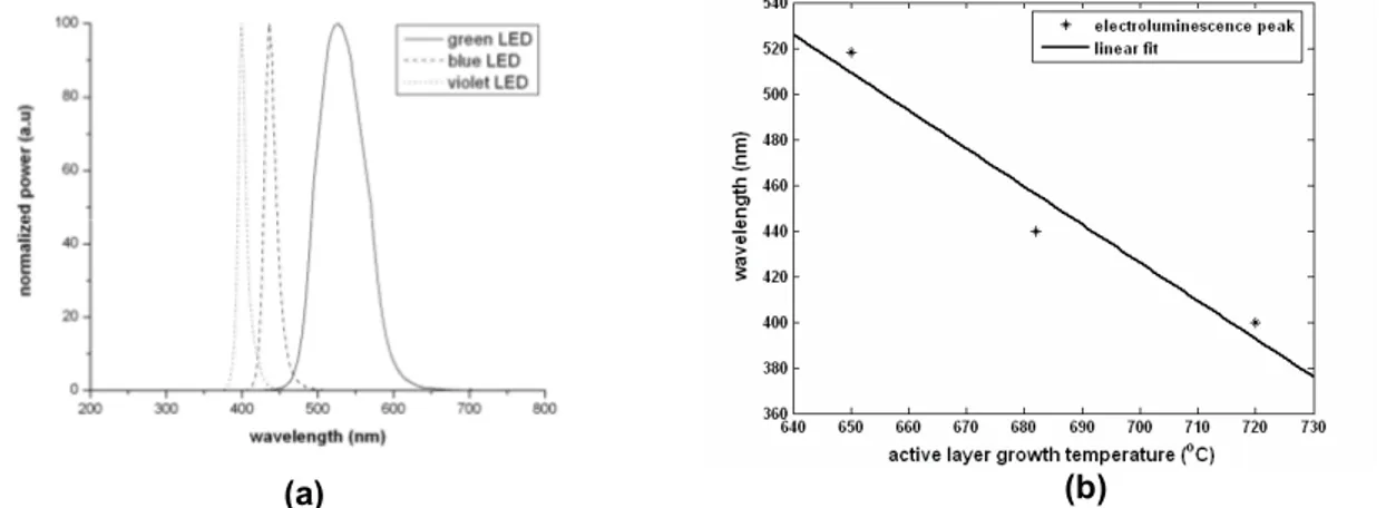
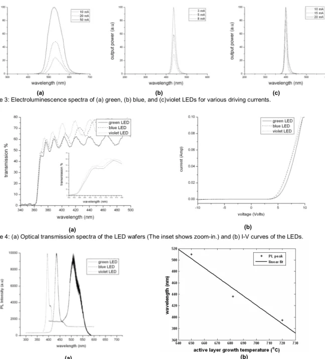
Figure 2a shows the electroluminescence (EL) spectra of the devices. EL peak shows a clear shift with the active layer growth temperature and exhibits a linear dependence on the temperature given by λ=1592-1.7T, where T is the active layer growth temperature in Celcius. The detected optical power for these devices exceeds 0.012 mW, 0.35 mW, and 0.245 mW for green, blue, and violet LEDs, respectively, for the same driving current level of 20 mA. The LEDs show increasing peak power with the increasing level of driving current as plotted in Fig. 3 (a, b, c).
(a) (b)
Figure 2: (a) Electroluminesce spectrum of the green, blue, and violet LEDs and (b) electroluminescence peak wavelength vs. active layer growth temperature, along the linear fit.
34 MC3
14:15 – 14:30
We also confirmed our spectral EL results with the transmission measurements shown in Fig. 4a. The relative positions of the bandedges show good agreement with the EL peak wavelengths. Photoluminescence (PL) measurements depicted in Fig. 5a also match the EL and transmission results. We find that the PL peak wavelengths depend on the growth temperature, again obeying the linear behavior λ=1600-1.6T, as sketched in Fig. 5b.
In conclusion, we report the epitaxial growth, fabrication, and characterization of violet, blue, and green LEDs based on a single InGaN/GaN quantum design with its EL peak (518nm-440nm-400nm) adjusted by the growth temperature (650°C-682°C-720°C, respectively). The EL, PL, and optical transmission measurements show good agreement, all revealing the linear dependence of the emission wavelength on the growth temperature.
(a) (b) (c)
Figure 3: Electroluminescence spectra of (a) green, (b) blue, and (c)violet LEDs for various driving currents.
(a) (b)
Figure 4: (a) Optical transmission spectra of the LED wafers (The inset shows zoom-in.) and (b) I-V curves of the LEDs.
(a) (b)
Figure 5: (a) Photoluminescence spectra of the LEDs and (b) PL peak wavelengths vs. active layer growth temperature, along with its linear fit.
Acknowledgements: This work is supported by EU MOON, EU NOE PHOREMOST and TUBITAK 104E114, 106E020, 105E065, and 105E066. H.V.D., E.O., and S.N. also acknowledge additional support from Turkish Academy of Sciences and TUBITAK.
References
[1] S. Nakamura, et al., Jpn. J. Appl. Phys., 34, 797 (1995).
[2] S. Nakamura, et al., The Blue Laser Diode: The Complete Story, Springer, NY (2000).