MICROSCOPIES
a thesis
submitted to the department of physics and the institute of engineering and science
of b˙Ilkent university
in partial fulfillment of the requirements for the degree of
master of science
By
Co¸skun Kocaba¸s
July 2003
Prof. Atilla Aydınlı (Supervisor) I certify that I have read this thesis and that in my opinion it is fully adequate, in scope and in quality, as a dissertation for the degree of Master of Science.
Assoc. Prof. Recai Ellialtıoˇglu I certify that I have read this thesis and that in my opinion it is fully adequate, in scope and in quality, as a dissertation for the degree of Master of Science.
Prof. H¨useyin Zafer Durusoy
Approved for the Institute of Engineering and Science:
Prof. Mehmet Baray,
INTEGRATED OPTICAL DISPLACEMENT SENSORS
FOR SCANNING FORCE MICROSCOPIES
Co¸skun Kocaba¸s
M. S. in Physics
Supervisor: Prof. Atilla Aydınlı
July 2003
In this thesis, we have studied the use of integrated optical waveguide devices acting as integrated displacement sensors on cantilevers for scanning probe microscopes. These displacement sensors include integrated optical waveguide devices such as Bragg gratings, ring resonators, race track resonators and waveguide Michelson interferometers fabricated on a cantilever to measure the displacement of the cantilever tip due to the forces between surface and the tip. The displacement of the cantilever tip is measured directly from the change of the transmission characteristics of the optical device. As the cantilever tip displaces, the stress on the cantilever surface changes the refractive index of the materials that make up the integrated optical device which cause variations in its optical transmission characteristics. We have also studied an optical waveguide grating coupler fabricated on the cantilever for the same purpose. In two different embodiments of this device, light is either coupled in or out of the waveguide via the waveguide grating coupler. The displacement of the cantilever alters the direction of the scattered light and measuring the power of the scattered light with a position sensitive detector allows for the detection of cantilever
Keywords: Scanning Probe Microscopy, Scanning Force Microscopy, Mach-Zehnder interferometer, Ring resonator, Grating coupler, Displacement sensor, Integrated optics, Waveguide sensors.
TARAMALI UC
¸ M˙IKROSKOPLARI ˙IC
¸ ˙IN T ¨
UMLES¸˙IK OPT˙IK
ALGILAYICILAR
Co¸skun Kocaba¸s
Fizik Y¨uksek Lisans
Tez Y¨oneticisi: Prof. Atilla Aydınlı
Temmuz 2003
Bu tezde, t¨umle¸sik optik ı¸sık kılavuzu aygıtlarının taramalı u¸c mikrosko-plarında algılayıcı olarak kullanılması incelendi. Bragg kırınım aˇgı, halka ¸cınlacı, Mach-Zehnder giri¸sim ¨ol¸cerinden olu¸san bu algılayıcılar d¨uzlemsel yay ¨uzerine imal edilip y¨uzey ve iˇgne arasında olu¸san kuvvet nedeniyle sapmasını ¨ol¸cmek i¸cin kullanılmaktadır. D¨uzlemsel yayın sapması, ¨uzerine monte edilmi¸s optik aygıtın ı¸sık ge¸cirgenliˇgindeki deˇgi¸simden faydalanılarak ¨ol¸c¨ulmektedir. D¨uzlemsel yaya takılı olan iˇgnenin haraketi sırasında d¨uzlemsel yayın y¨uzeyinde olu¸san zor, optik aygıtın kırınım indisini deˇgi¸stirmesi sonucu optik ge¸cirgenlikteki deˇgi¸simlere sebep olmaktadır. Benzer ¸sekilde optik dalga kılavuzu kırınım aˇgı ¸cifleyicileri de algılayıcı olarak kullanılmı¸stır. Bu aygıtlar i¸ceri ve dı¸sarı ¸cifleyici olmak ¨uzere iki farklı durumda incelenmistir. D¨uzlemsel yayın sapması sonucu sa¸cılan ı¸sıˇgın doˇgrultusunda deˇgi¸smeler olu¸smakta ve sa¸cılan ı¸sıˇgın ¸siddeti konum duyarlı fotodetekt¨or ile ¨ol¸c¨ulebilmektedir. ¨Onerilen bu yeni tasarım sayesinde 10−4˚A−1 seviyesinde duyarlılık elde etmek m¨umk¨und¨ur.
optik, Dalga kılavuzu algılayıcıları .
I would like to express my deepest gratitude to Prof. Atilla Aydınlı for his guidance, moral support, friendship and assistance during this research.
I would also like to thank to Prof. A. Oral and Prof. Nadir Daˇglı from whom I have learned a lot.
I would like to thank my twin brother A¸skın for his help that has been invaluable for me.
I would like to thank ˙Isa Kiyat for his help during this work especially analysis of ring resonator.
I would like to thank Mehrdad Atabak from whom I have learned the principles of AFM.
I would like to thank to all Integrated Optics Group members Feridun Ay, ˙Isa Kiyat, A¸skın Kocaba¸s, Selcen Aytekin , ˙Imran Ak¸ca and Nuh Sadi Y¨uksek for their friendship and to keep my sprits high.
Ertuˇgrul C¸ ubuk¸cu, Engin Durgun, Deniz C¸ akir, Cem Sevik, Turgut Tut, Sinem Binicioˇglu, Ercan Avcı, Mustafa Kesir, S¨uleyman Tek, Necmi Bıyıklı helped to keep my spirits high all the time which I appreciate very much.
I am indebted to my family for their continuous support and care.
Abstract i ¨ Ozet iii Acknowledgement v Contents vi List of Figures ix
List of Tables xiii
1 Introduction 1
1.1 Scanning Probe Microscopy . . . 1
1.2 Displacement Sensors for SPM . . . 2
1.2.1 External Deflection Sensing Systems . . . 3
1.2.2 Integrated Deflection Sensing Systems . . . 4
1.3 Aim of This Study . . . 6
2 Theoretical Considerations 7 2.1 Overview of the Integrated Optical Sensors . . . 7
2.2 Design of the Waveguide Structures . . . 9
2.3 Beam Propagation Method . . . 12
2.4 Photo-elastic Effect . . . 13
2.5 Finite Element Method Analysis . . . 16
2.7 Transfer Matrix Method . . . 23
3 Mach-Zehnder Interferometers 27 3.1 Physical Considerations . . . 28
3.2 Mach-Zehnder Interferometer as a Displacement Sensor . . . 30
3.3 Waveguide Design . . . 33 3.4 Sensitivity Analysis . . . 34 3.5 Experimental Setup . . . 35 4 Bragg Gratings 36 4.1 Operation Principles . . . 37 4.2 Cantilever Design . . . 39
4.3 Bragg Grating Design . . . 41
4.4 Quarter-wave Shifted Bragg Grating . . . 44
4.5 Experimental Setup . . . 46
4.6 Sensitivity . . . 47
5 Micro-Ring Resonators 50 5.1 Physical Considerations . . . 50
5.2 Analysis and Design of Micro-Ring Resonators . . . 53
5.2.1 Ring Resonator Analysis: Single Bus System . . . 53
5.2.2 Ring Resonator Analysis: Double Bus System . . . 56
5.2.3 Waveguide Design . . . 56
5.2.4 Ring Resonator as Displacement Sensor . . . 58
5.3 Sensitivity Analysis . . . 61
6 Grating Couplers 65 6.1 Input and Output Grating Coupler . . . 66
6.2 Input and Output Grating Coupler as a Displacement Sensor . . . 70
7.3 Detector Noise . . . 78
8 Conclusions and Suggestions 81
2. 1 Different types of optical waveguides . . . 9 2. 2 Schematics of slab waveguide with refractive index of nf, ns, nc for
film, substrate and cover, respectively . . . 10 2. 3 Directions of electric and magnetic for Transverse Electric (TE)
and Transverse Magnetic (TM) polarization . . . 10 2. 4 (a)Geometry of the waveguide and (b) electric field distribution of
single mode GaAlAs/GaAs waveguide. nGaAlAs = 3.00, nGaAs =
3.37 . . . . 14 2. 5 Index ellipsoid and propagation direction of a wave . . . 15 2. 6 (a) Cantilever structure, (b) meshed geometry, (c) stress
distribu-tion on the cantilever for 100 ˚A displacement. . . . 21 2. 7 Longitudinal stress distribution on the cantilever, stress reaches
its maximum value at the supporting point of the cantilever and decreases linearly along the cantilever. . . 22 2. 8 Waveguide Bragg grating and its layer modelling . . . 24 2. 9 Electric field for three layers with different refractive index . . . . 24 3. 1 Schematics of Mach-Zehnder interferometer . . . 28 3. 2 Output intensity of Mach-Zehnder interferometer as a function of
the phase shift. Small variation of the phase shift results in the output intensity variation, at the quadrature point (Φ = π/2) maximum variation can be achieved . . . 29 3. 3 Schematic of Mach-Zehnder interferometer integrated on a cantilever. 31
the two arm in order to achieve steepest slope at z = 0 . . . . 32 3. 5 Waveguide structure for Mach-Zehnder interferometer w = 1µm
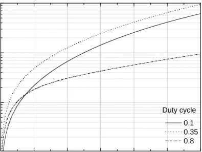
and H = 0.75µm . . . . 33 3. 6 Y junction . . . 34 4. 1 Schematics of cantilever integrated with a Bragg grating. . . 39 4. 2 Calculated coupling coefficient as a function of grating height for
three different duty cycles. . . 43 4. 3 Calculated coupling coefficient as a function of duty cycle. . . 44 4. 4 Calculated reflection spectrum for 250 µm long Bragg grating with
0.210 µm period and 0.1 µm grating height. . . . 45 4. 5 Calculated transmission spectrum for quarter-wave shifted Bragg
grating. Very narrow transmission band can be achieved (∆λ = 0.5˚A) . . . 46 4. 6 The normalized output intensity variation as a function of the
index change of the grating for different cavity lengths. Where L1,
L2, L3, L4 are 101λ4, 201λ4, 301λ4, 501λ4, respectively. . . 47
4. 7 The normalized output intensity variation as a function of the cantilever displacement for 200 and 1000 µm long cantilevers thickness of 5 µm and width of 50 µm. . . . 48 5. 1 Sensor concept based on a ring resonator. The optical power
modulation takes place as position of resonance dip shifts. Inset shows the variation of the output intensity. . . 51 5. 2 A schematic illustration of the operational principle for the
integrated micro-ring resonator displacement sensor, (a and c) shows the cantilever for unbent and bent condition, (b and d) shows the field distribution on the ring resonator on the cantilever. 52 5. 3 Schematic representation of single bus (a) and double bus (b) ring
resonator and the relevant propagating field amplitudes. . . 54
race-track resonators are useful for increasing the accumulated phase shift. . . 59 5. 6 Calculated stress distribution on the ring resonator as a function
of the angle as measured from the major symmetry axis of the cantilever. . . 60 5. 7 Transmission spectrum of single bus and double bus ring resonators
for both with (SBcr and DBcr) and without (SB and DB) critical
coupling condition is achieved, respectively. The increase in steepness of the dips when critical coupling is achieved is clearly observed. . . 62 5. 8 Transmitted intensity variation with cantilever displacement for
single and double bus ring resonator with (SBcr, DBcr ) and
without (SB, DB) critical coupling condition achieved. The best results are obtained under critical coupling condition. . . 63 5. 9 Sensitivity vs wavelength for single bus with critical coupling
achieved. . . 64 6. 1 Schematics of the input grating coupler, amplitude of the incident
light is shown with a Gaussian. function . . . 66 6. 2 k-space diagram of the input grating coupling diffracted, refracted
and guided modes are shown. . . 67 6. 3 Normalized coupling efficiency versus incidence angle for a grating
coupler with 300 grooves. . . 68 6. 4 Schematics of an output grating coupler. . . 69 6. 5 Scattering mechanism of an output grating coupler . . . 70 6. 6 Schematics of a cantilever integrated with an input grating coupler 71 6. 7 Normalized normalized coupling efficiency vs incidence angle for
gratings of length of 200 µm and 400 µm . . . 71 6. 8 Normalized output intensity vs cantilever displacement. . . 73
8. 1 1D array of cantilever integrated with grating output coupler (a) and input coupler (b). . . 82
2.1 Stress optic coefficients for waveguide materials. . . 16 2.2 Mechanical properties of some materials. . . 19 3.1 Calculated displacement sensitivities. . . 35 5.1 Calculated displacement sensitivities for single and double bus ring
resonators with (SBcr, DBcr) and without (SB, DB) critical coupling. 63
7.1 Calculated displacement sensitivities and shot noise limited minimum detectable distances for 100µW optical power and 1 kHz band width. . . 80
Introduction
1.1
Scanning Probe Microscopy
Scanning probe microscope (SPM) is an instrument that measures the spatial variation of the local properties of a surface. SPM is a very powerful tool to produce highly detailed three dimensional images of a surfaces. Not only the topographic image but also other images of physical properties such as friction forces, temperature, magnetic field, electric field and charge of the surface can be determined using different configurations of the SPM.
The most important parameter for a microscope is the resolution. Resolution (or strictly speaking resolving power) is defined as the closest spacing of two points which can be resolved by a microscope to be separate entities. The resolution of conventional optical microscopes are limited by the diffraction of light and is typically of the order of a micrometer. In the 1930s, electron microscopes were developed which uses an electron beam instead of light rays and nanometer order resolution was obtained. However, the atomic scale resolution was still impossible. In 1982 Gerd Binning and Heinrich Rohrer [1] invented the scanning tunnelling microscope (STM) and they achieved atomic resolution and they were awarded the Nobel Price. Invention of STM has stimulated the development of more than two dozen types of SPMs. Atomic force microscope (AFM) [2] , lateral force microscope (LFM) [3] , magnetic force microscopes (MFM) [4] , near field
scanning optical microscope (NSOM) [5] are some of the different aspects of the SPM.
The main principles of the scanning force microscopes are similar, a sharp pyramidal tip mounted on a cantilever is brought close proximity to the surface and attractive or repulsive forces between the surface and the sharp tip causes the cantilever to bend. Monitoring the bending of the cantilever, it is possible to determine the image of the surface. The key component of the force microscope is a cantilever with the tip. The tip must be sharp enough to achieve high resolution and the cantilever must have appropriate properties for the type of operation selected. Three types of operations are most commonly used: 1) contact mode, the tip contacts with the surface and the force constant of the cantilever has to be low enough to avoid the damage on the sample, 2) non-contact mode, the tip is brought in close in proximity of the surface and vibrates near its resonant frequency, for which large force constant cantilevers are preferred and 3) intermittent contact mode, here the cantilever vibrates with its resonant frequency and the tip periodically touches the surface for which cantilevers with high force constant are preferred [6].
1.2
Displacement Sensors for SPM
Many scanning probe microscopies require the measurement of the displacement of the cantilever with high sensitivity. A good example is scanning force microscope [2] , based upon the principle of sensing the forces between a tip and a surface. These forces induce the displacement of the tip mounted on the cantilever. There is a great need to determine the displacement of the cantilever with high sensitivity to work out the attractive and repulsive forces between surface and the tip. There are many different deflection sensing systems to determine the cantilever deflection. These systems can be categorized into two main groups; external and integrated deflection detection systems. All these systems have advantages and disadvantages over each other. In this chapter, some of these systems will be discussed briefly. There are many other methods
and the detailed information can be found in the reference cited [7] .
1.2.1
External Deflection Sensing Systems
External detection systems use external physical components to measure the deflection of the cantilevers. In this section, principles advantages and disadvantages of some of these methods will be discussed. External systems are commonly used due to their high sensitivity, however these techniques require the use of precisely aligned optical components which limits the surface area and they are not very suitable for UHV environment due to their complexity.
Optical Lever Detection
Most widely used technique is the optical lever technique [8,9] . In this technique, an external collimated laser light is reflected from the cantilever surface and detected with a position sensitive detector (PSD). PSD is placed at a large distance from the cantilever. A differential amplifier is used with the PSD. As the cantilever deflects, the intensity of the light falling on the detectors differs and by monitoring the output of the differential amplifier, which is a linear function of the cantilever displacement, it is possible to detect the displacement. The resolution of this method is about 0.1 ˚A. Although this method is very simple
and cheap, it has low sensitivity and requires alignment during the surface scan and it is not very suitable for cantilever arrays.
Interferometric Detection
A highly sensitive technique is the interferometric detection which uses a cleaved end of an optical fiber and the back side of the cantilever as a Fabry-Perot interferometer [10–12] . As the cantilever displaces, the spacing between the fiber and cantilever surface differs and the reflection spectrum of the Fabry-Perot changes. The reflected light produces a photocurrent on the photo-detector and this photocurrent is used to image the force acting on the tip. Using this technique, it is possible to achieve ± 0.01˚A resolution, however, it requires
accurately positioning the fiber to the cantilever and keeping the alignment during the surface scan which limits the scan area and this method is also not suitable for cantilever arrays.
Tunnelling Detection
This method was firstly used by Binning et. al. [2] Tunnelling detection
method uses the tunnelling of the electrons from the conducting cantilever to the conducting tip. The application of the bias voltage between tip and cantilever produces a tunnelling current though the air gap. Tunnelling current exponentially decreases with the tip-cantilever separation. Tip-cantilever separation is about several angstroms. As the cantilever displaces, the tunnelling current decreases, and by monitoring the tunnelling current it is possible to determine the cantilever displacement.
Interdigital Detection
A further method is to use two sets of interdigitated fingers [13,14] , one reference set being attached to the substrate from which the cantilever extends and the other movable set being attached to the tip of the cantilever. The interdigitated fingers form an optical phase grating. The deflection of the cantilever is measured by directing a light beam onto the optical phase grating and measuring the diffracted light in reflection. This method provides the highest sensitivity up to date, ± 0.002 ˚A resolution is possible however, it requires alignment of laser
beam and also the photo-detector. This method was also demonstrated for 5 × 1 cantilever arrays.
1.2.2
Integrated Deflection Sensing Systems
Integrated deflection sensing systems use an integrated sensor on a cantilever and measure the changes in a physical property of the sensor due to the bending of the cantilever. These sensors are very compact and they are individually addressable which allows them to be used in cantilever arrays. The main problem
of the integrated sensors is their sensitivity. They generally have two orders of magnitude less sensitivity than the external sensors. There is still the need to have highly sensitive integrated sensors.
Piezo-resistive Sensors
This method was firstly introduced by Tortonese et. al. [6] in 1991. Piezoresistive effect was used for sensing mechanism. The variation of resistivity with applied stress is known as piezoresistive effect. A piezoresistive element integrated on the cantilever is used to sense the generated stress on the surface due to the bending of the cantilever. This method is very compact and it does not require any alignment and also it is suitable for cantilever arrays, but it has three orders of magnitude less sensitivity than the other methods.
Piezoelectric Sensors
In this method [16], a cantilever made up of piezoelectric material, such as lead zirconate titanate (PZT), zinc oxide (ZnO), piezoelectric polymer (PVDF), is used , or piezoelectric film is sputtered on a cantilever and electrodes are made on the upper and lower surface. As the cantilever displaces, a voltage is generated between the electrodes due to piezoelectric effect. By measuring the generated voltage it is possible to determine the cantilever displacement. This method can also be used as an integrated actuator to control the cantilever displacement. Integrated Transistor Sensors
An integrated MOS transistor was used as a force sensor by Akiyama et al. [17] in 1998. When the channel of the MOS transistor is subjected to stress, the carrier mobility changes, resulting in a changing source-drain current. The MOS transistors and read out circuit can be fabricated with conventional CMOS process. The channel of the transistor is at the surface, where stress gets its maximum value, therefore the sensitivity of this sensor is slightly higher than the piezoresistive sensors.
Capacitive Sensors
This method uses the capacitive lever displacement detection [18, 19]. Force induced cantilever displacements yields capacitive changes by changing the electrode spacing. Compared to the other integrated sensors, this sensor has high sensitivity. Capacitive detection is also interesting because it is free of parasitic resistive noise.
1.3
Aim of This Study
The main goal of this thesis work is to design and analyze highly sensitive integrated optical waveguide sensors for scanning probe microscopes to measure cantilever displacement. It is another objective of this thesis work to provide displacement sensors compatible with cantilever arrays which are suitable for nano-lithography systems and data storage technology. The novel design proposed in this work provide displacement sensors which do not require any tedious alignment of laser. The advantage of the present sensors over the prior work is that they provide for simple and compact integrated optical waveguide displacement sensors that measure the cantilever displacement without any or little alignment.
Theoretical Considerations
This chapter is devoted to theoretical background for the design of integrated optical displacement sensors. Formalism and the basic principles of the computational methods which will be extensively used during the next chapters will be studied.
2.1
Overview of the Integrated Optical Sensors
The fiber optic and integrated optic technologies for measurement systems is very attractive. The integrated optic (IO) sensors have many advantages over their electronic counterparts. The main advantage of IO sensors is that it is possible to fabricate several components on a single chip which provides very compact and stable systems. Guided wave structures are immune to electromagnetically active environments and they have higher sensitivity than the electronic sensors. Recently, there have been many studies on the IO pressure sensors, bio-sensors, temperature sensors and strain sensors. These sensors consist of integrated optical devices such as Mach-Zehnder interferometers [20] , Michelson interferometers [21] , Bragg gratings [22] , directional couplers [23] , and ring-resonators [24] , whose transmission characteristics change due to external effects. The integrated optic sensors mostly use the two beam interference structure. An external physical value to be measured induces a phase
shift between two guided beams and this phase shift produces intensity change at the output of the sensor. By monitoring the intensity changes the external physical value is measured.
In this thesis, we introduce integrated optical detection method for scanning force microscopies. In the first chapter, different detection mechanisms were discussed. Considering other detection methods, integrated optical method has many advantages over others. First, an integrated sensor does not require any alignment of the laser and detector during surface scanning and it is possible to scan large areas. Second, integrated sensors are suitable for cantilever arrays due to their compactness, simplicity and potential for mass production. Another important aspect of the integrated sensors is that they provide individually addressable operation. It should also be mentioned that integrated sensors such as piezo-resistive ones [6] have less sensitivity (about 10−7˚A−1) than
the external sensors such as optical levers [8] (about 10−5˚A−1). Using an
integrated optical sensor, we expect to achieve as high sensitivity as external sensors. Integrated optical devices can be inexpensive and they can be used in harsh environments such as UHV systems and electromagnetically active environments. Integrated optical method is based on the detection of the changes of the transmission characteristics of an integrated optical devices due to the deflection of the cantilever. We will apply different types of integrated optical devices for displacement detection. Basically, we can categorize these devices into two groups: in the first group, transmission characteristics of the optical device, which is integrated on the cantilever, changes due to the photo-elastic effect and elongation of the optical path, in the second group the transmission characteristics changes due to the change of the coupling efficiency which alters the transmission of the optical device. In this chapter, theoretical background and formalism will be given and in the next chapters analysis of different types of integrated optical devices such as, Mach-Zehnder interferometer, Michelson interferometer, micro-ring resonator, Bragg grating and grating input and output coupler will be discussed thoroughly.
2.2
Design of the Waveguide Structures
Waveguide structures are the central part of the integrated optical devices. Detailed analysis of waveguide structures can be found in the references cited [25, 26] . In this section basic principles of the waveguide structures and the design for the sensor application will be discussed. Basically, thin films deposited on a dielectric substrate are used as optical waveguide if the film refractive index is higher than the substrate index. Basic waveguide structures are given in the Figure 2. 1. The simplest optical waveguide structure is the step-index slab waveguide. The slab waveguide consists of a high index dielectric layer surrounded with low index dielectric layers. The guiding layer has a finite thickness in the x direction and infinite in yz plane which is shown in Fig. 2. 2. In order to achieve total internal reflection in the guiding layer, the index of refraction of the substrate and the cover layer must be smaller than the guiding layer. If the cover and the substrate materials have the same index of refraction, this waveguide is called a symmetric, otherwise it is called an asymmetric waveguide. The electromagnetic analysis of the optical waveguide structures
Figure 2. 2: Schematics of slab waveguide with refractive index of nf, ns, nc for
film, substrate and cover, respectively
E
H
k
k
E
H
x
z
Transverse Electric
(TE)
Transverse Magnetic
(TM)
.
Figure 2. 3: Directions of electric and magnetic for Transverse Electric (TE) and Transverse Magnetic (TM) polarization
are based on the solving the Maxwell equations using the suitable boundary conditions. The solution of the Maxwell equations gives the specific propagation direction and the electromagnetic field distributions which is called modes of the waveguide. Consider an asymmetric waveguide such that nf > ns > nc
with the guiding layer thickness of h. During the analysis we choose z as the propagation direction and x as the normal direction of the waveguide plane. For slab waveguide, rectangular coordinate system is the most suitable coordinate system because the electromagnetic fields can be uncoupled to Ex, Ey and Ez
which simplifies the analytic solution. The orientation of the electric fields have two different polarizations, transverse electric (TE) and transverse magnetics (TM). Figure 2. 3 depicts the two different polarizations for slap waveguide.
First, we will solve wave equation for TE polarization and the solution for the TM polarization is similar when the electric fields are replaced with magnetic fields. For TE polarization E field is polarized along the y direction and the light source which excite the waveguide has the frequency of w0. In order to find the
allowed modes for the waveguide, wave equation must be solved for each layer and they must be combined with the boundary conditions. The wave equation for electromagnetic waves in a dielectric medium can be written as
∇2E
i− µε
∂2E
i
∂t2 = 0 (2. 1)
Here the subscription refers to the ithcomponent. To find the solution, we have to
use the separation of variables techniques in cartesian coordinate system and we get the scalar wave equation for each component and we expect the trial solution as
Ey(x, z, t) = Eye−jβizejw0t (2. 2)
where βi is the propagation coefficient along the z direction. Inserting the trial
solution into the Eq. 2. 1, we get
∂2E
y
∂x2 + (k 2
0n2i − β2)Ey = 0 (2. 3)
We have to solve this equation for three layers with the refractive indices ns, nc, nf.
From the Eq. 2. 3 we get the transverse field amplitude in the exponential form. Two cases must be considered, i) β > k0ni and ii) β < k0ni. For β > k0ni
transverse field amplitude, which is called the evanescent field, is
Ey = E0e± √ β2−k2 0n2i (2. 4) and for β < k0ni Ey = E0e±j √ k2 0n2i−β2 (2. 5)
which is an oscillating field. Our aim is to find the allowed β values. In order to do this we should write the field amplitudes for three layers and matching them at the boundaries considering the continuity of the tangential electric and
magnetic fields. The field amplitudes for three layers are
Ey(x) = Ae−γcx 0 < x (2. 6)
Ey(x) = Bcos(κx) + Csin(κx) − h < x < 0
Ey(x) = Deγsx x < −h
where A,B,C,D are the coefficients to be determined. Applying the boundary conditions at the two interfaces, we get a transcendental equation for β,
tan(hκf) = γc+ γs κf(1 − γκcγ2s f ) (2. 7) here γ = qβ2− k2 0n2i and κ = q k2
0n2i − β2. The solution of the Eq. 2. 7
gives discrete values of β. The physical meaning of β is the component of the wavevector along the propagation direction. This means that the guided light propagates at certain angles along the z direction.
2.3
Beam Propagation Method
In the previous section we have defined the fundamentals of the optical waveguides. In this section we will describe the numerical solutions for more complicated structures using Beam Propagation Method (BPM). BPM is the most widely used propagation technique for modelling the integrated and fiber optic photonic devices. For device simulation we have used commercial software package BeamPROP [27]. In the BPM the exact wave equation is approximated for monochromatic waves and it is solved numerically. By neglecting the polarization of the wave, we get a three-dimensional scalar wave equation (Helmholtz Equation) which is the fundamental equation to be solved by BPM. The scalar wave equation is written as
∂2E ∂x2 + ∂2E ∂y2 + ∂2E ∂z2 + k 2n(x, y, z)2 = 0 (2. 8)
Electric field can be separated in two parts; the envelope term Φ(x, y, z) which is a slowly varying function and the rapidly varying term e−jkn0z where z
is the propagation direction. Another approximation is the weakly guiding approximation (n2 − n2
0) = 2n0(n − n0). Substituting these in to the Eq.2. 8
we get ∂Φ ∂z = −j 1 2kn0 ∇2Φ − jk(n − n0)Φ (2. 9)
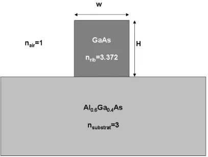
This equation is solved by standard numerical techniques. Firstly Φ is defined only as discrete points on a grid. Differentiation is defined as finite differential and the goal is to derive the numerical equation that determines the fields at the next z plane. Gaussian launch field is taken as initial field at the initial z plane and using the numerical equation the field is propagated along the z direction. BPM provides accurate results under certain conditions. These conditions are that, the refractive index of the device must be slowly varying function of z and the propagation is restricted to a narrow range of angles. S-shaped bend waveguides, tapered waveguides, directional couplers, branching and combining waveguides can be simulated. Also the modes of a waveguide (field distributions) can be obtained. Fig.2. 4 illustrates the electric field distribution of an GaAlAs/GaAs waveguide structure obtained from BPM. More detailed information can be found in the references cited [28].
2.4
Photo-elastic Effect
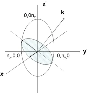
Photo-elastic effect is the change in the refractive index of a material under applied stress. This phenomenon was first discovered by Sir David Brewster in 1815 and systematically investigated by Pockel. During the investigation of the photo-elastic effect, formalism of index ellipsoid plays the central part. Index ellipsoid defines an ellipse in which the distance from the origin to the surface of the ellipsoid represents the magnitude of the refractive index of the crystal in any direction. Figure 2. 5 represents the index ellipsoid where k is the wavevector and x0, y0, z0 represents the principle directions in the crystal. Equation for the
-2.0 -1.5 -1.0 -0.5 0.0 0.5 1.0 1.5 2.0 -1.0 -0.5 0.0 0.5 1.0 V e rt ica l D im e n si o n Horizantal Dimension (µm) (a) (b)
Figure 2. 4: (a)Geometry of the waveguide and (b) electric field distribution of single mode GaAlAs/GaAs waveguide. nGaAlAs= 3.00, nGaAs = 3.37
ellipsoid can be written as
x02 n2 x + y 02 n2 y +z 02 n2 z = 1 (2. 10)
If a wave propagates in k direction, the effective index for the wave depends on the polarization of the electric fields, and it lies in the circle shown in the Figure 2. 5. When external stress applied on the material, the dielectric tensor (1
n2) is
transformed like a second rank tensor and it can be written as ∆( 1 n2)i = 6 X j=1 pi,jSj (2. 11)
where pi,j represents the strain optic coefficients and Sj represents the present
Figure 2. 5: Index ellipsoid and propagation direction of a wave respectively. From Eq. 2. 11 we can get
∆n = −n3 2 6 X j=1 pi,jSj (2. 12)
Strain can also be written in terms of the stress components and we can write Eq.2. 12 in terms of the stress and we get
∆ni =
6
X
j=1
Cj,iσj (2. 13)
where Cj,i are the photo-elastic coefficients and σi are components of the stress.
For isotropic medium Cj,i have two different values; longitudinal photo-elastic
constant CL and transverse photo-elastic constant CT. Using these constants, we
can write refractive index changes for each direction as,
∆nx = CLσx+ CT(σy+ σz) (2. 14)
GaAs Si SiO2 Si3N4
CL (P a−1) 1.7 10−11 1.56 10−11 −0.75 10−12 −5.3 10−12
CT (P a−1) 1.0 10−11 −0.45 10−11 −4.1 10−12 −1.8 10−12
Table 2.1: Stress optic coefficients for waveguide materials.
∆nz = CLσz+ CT(σy + σx) (2. 16)
CL and CT can be written as
CL = −n3 2E (p11− 2νp12) (2. 17) CT = −n3 2E (−νp11+ (1 − ν)p12) (2. 18)
where p11 and p12 are the strain optical coefficient, n is the refractive index, E is
the Young’s Modulus and ν is the Poisson ratio of the material. We can make an analogy between the photo-elastic effect and the electro-optic effect. They both deform and rotate the index ellipsoid, but whereas photo-elastic effect is universal and it can be observed in symmetric and asymmetric crystals such as Si and GaAs, electro-optic effect can only be observed in asymmetric crystals (without inversion symmetry) such as GaAs (not Si). Quadratic electro-optic effect (Kerr effect) is also universal like as photo-elastic effect [29]. In Table 2.1 we summarize the stress optic coefficients for different materials. GaAs and Si have large stress optic coefficients.
2.5
Finite Element Method Analysis
Finite Element Method (FEM) was firstly developed for the stiffness analysis of airplanes. Stress analysis is the most common application of FEM. There are many formulations that are used to solve FEM problems. Two of them are minimum total potential energy formulation, weighted residual formulation . We have used total potential energy formulation (TPEF). TPEF is the common
method for solid mechanics. When the external forces applied on a structure, structure deforms and the work done by the external forces is stored as elastic energy (strain energy). Deformation of the solid (displacement) can be written as
~δ = u(x, y, z)ˆi + v(x, y, z)ˆj + w(x, y, z)ˆk (2. 19) Strain vector has six components and can be written from the displacement as
εxx = ∂u ∂x (2. 20) εyy = ∂v ∂y εzz = ∂w ∂z γxy = ∂u ∂y + ∂v ∂x γyz = ∂v ∂z + ∂w ∂y γxz = ∂u ∂z + ∂w ∂x
For elastic materials there is a relationship between stress and strain according to the Hooke’s Law and given by the following equation
εxx = 1 E[σxx− υ(σyy− σzz)] (2. 21) εyy = 1 E[σyy− υ(σxx− σzz)] εzz = 1 E[σzz− υ(σxx− σyy)] γxy = 1 Gτxy γyz= 1 Gτyz γzx= 1 Gτzx
where E is the Young’s modulus and G is the shear modulus. Potential energy can be written as (strainenergy) = 1 2 Z (stress)T(strain)dV (2. 22)
The main goal is to minimize this integral equation. Structure is firstly discretized into small elements and the solution of the problem is approximated in each element with suitable shape functions and the unknown constant (to be determined) at the nodal points. Applying this approximation and minimizing the integral by taking the derivative for each unknown constant, the entire problem is reduced to a matrix equation. The most important thing that has to be considered is the shape function and the element shape. More detailed information can be found in the references cited [26, 31].
2.5.1
Cantilever Design
Fundamental mechanical parameters of an AFM cantilever are its spring constant and resonant frequency. The optimal values of these parameters depend on the mode of the operations, namely contact mode, non-contact mode, and intermittent contact mode. GaAs has a large photo-elastic constant which makes it a suitable material for fabrication of integrated optical devices and cantilever. Other materials such as Si3N4 and Si can also be used with varying sensitivities.
Our design is based on rectangular cantilevers which are compatible with well established micromechanical fabrication technology. For a rectangular cantilever, spring constant and resonant frequency can be written as,
k = Ewt3 4l3 (2. 23) and f0 = t l2( E ρ) 1/2 (2. 24)
respectively. Here E is the Young’s modulus, ρ is the density of the cantilever material and t is the thickness, l is the length, w is the width of the cantilever. Typical micromachined cantilevers for AFM have lengths of 100 µm to 400 µm,
GaAs Si SiO2 Si3N4
Y oung0sModulus (GP a) 85 130 75 85 − 105
P oisson Ratio 0.31 0.279 0.17 0.24 Table 2.2: Mechanical properties of some materials.
widths of 20 µm to 50 µm and thicknesses of 0.4 µm to 10 µm. A large spring constant is preferable for non-contact mode and intermittent mode operations. On the other hand, low force constant is preferable for contact mode operations. The resonant frequency is required to be a few kHz in order to minimize the external effects [48]. During the analysis we choose a rectangular cantilever length of 200 µm width of 50µm and thickness of 5 µm. The resonance frequency is 50 kHz, the spring constant is 16 N/m. In Table 2.2, mechanical properties of different materials are summarized.
2.5.2
Finite Element Method Stress Analysis of the
Cantilever
In any cantilever design, the measurement of the displacement of the cantilever with high sensitivity is the essential task. The design of the cantilever and the type of the integrated sensor plays a fundamental role to increase the sensitivity. Bending the cantilever generates stress which is the necessary physical quantity used to characterize the displacement of the cantilever. Photo-elastic effect is used for the sensing mechanism; stress generated on the cantilever changes the refractive index of the waveguide where the optical sensor is loaded. Furthermore, sensing the generated stress using integrated optical devices requires materials suitable for such devices with large stress optic coefficients. A good candidate is GaAs. Applying mechanical stress to GaAs results in variation of local index due to photo-elastic effect, therefore we will use GaAs as a cantilever material. Since the displacement of the tip causes mechanical stress along the cantilever, maximizing the stress on the sensing element will maximize the performance. Obtaining the generated stress is the essential task. The stress distribution on the rectangular cantilever can be written analytically. As the cantilever bends,
stress reaches its maximum value at the supporting point and decreases linearly along the cantilever. Therefore, the sensing element is placed at the supporting point where
σmax =
3Et
2l2 z (2. 25)
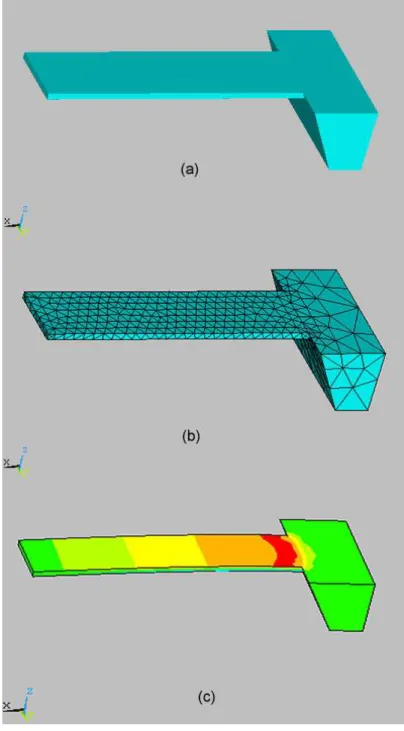
in which, E is the Young’s Modulus, t is the thickness, l is the length and z is the displacement of the cantilever. To obtain more accurate results for complicated geometries Finite Element Method (FEM) analysis is employed. We have used general purpose FEM software program ANSYS. FEM analysis consist of four steps of, drawing the structure, meshing, applying boundary condition, and solving the static equation. In Fig. 2. 6 these steps are illustrated. Fig. 2. 6a represent the cantilever with length of 200 µm, width of 50 µm and thickness of 5 µm. Cantilever is fixed to a substrate from one end and the other end is free. Fig. 2. 6 b represents the meshed geometry. The meshing has to be increased near the supporting point where the optical device will be placed. Fig. 2. 7 shows the stress distribution on the cantilever for 100 ˚A displacement. Longitudinal stress
is much larger than the transverse stress and in our calculation we can neglect the transverse stress. Longitudinal stress reaches its maximum value (1.5 105P a) at
the supporting point of the cantilever and decreases linearly along the cantilever. There is good agrement between the FEM results and the analytical expression for stress distribution.
2.6
Coupled Mode Theory
Coupled Mode Theory (CMT) will be used for the design of the grating to calculate the coupling coefficient. CMT describes how energy exchange occurs between two guided modes in an integrated optical device. There are much similarities between the perturbation theory in quantum mechanics and the CMT for integrated optics. In an ideal waveguide (no perturbation) the amplitude of a guided mode does not change along the waveguide. If there is a perturbation, the ideal mode starts to couple to other guided or radiative modes and the amplitude decreases. Consider a multi mode waveguide. For each mode transverse electric
Figure 2. 6: (a) Cantilever structure, (b) meshed geometry, (c) stress distribution on the cantilever for 100 ˚A displacement.
field amplitude can be written as
Eyi(x, z, t) = 1
2Aiξyi(x)e
-50 0 50 100 150 200 0.0 2.0x10⁴ 4.0x10⁴ 6.0x10⁴ 8.0x10⁴ 1.0x10⁵ 1.2x10⁵ 1.4x10⁵ 1.6x10⁵ S tr e ss (P a ) Distance (µm)
Figure 2. 7: Longitudinal stress distribution on the cantilever, stress reaches its maximum value at the supporting point of the cantilever and decreases linearly along the cantilever.
The subscription i represent different modes in the waveguide and Ai is the
amplitude and ξyi(x) is the normalized amplitude for the modes. If there is no change in the dielectric constant ( refractive index) or in the dimension along the waveguide, different modes do not couple each other, they are completely independent. If there is a perturbation, this makes the modes couple to each other and energy exchange starts. The perturbation can be in two different ways; refractive index may change along the waveguide or an electric field from a second source appears in the waveguide and it may excite the mode and the field amplitudes increases along the waveguide. Perturbation introduces an extra term in the electric flux. Electric flux for unperturbed condition can be written as
D = ²E = ²0E + P (2. 27)
Where P is the polarization in the dielectric. The effect of the perturbation increases the electric flux and the electric flux is modified as
if we substitute this equation into the wave equation we get ∇2Ey = µ² ∂2E y ∂t2 + µ ∂2P pert ∂t2 (2. 29)
If we substitute Eq.2. 26 in to this equation and with simple algebra we can drive the famous mode coupling equation between the modes which propagates in positive and negative directions as
∂A+i ∂z e j(βz+ωt)−∂A−i ∂z e j(βz+ωt)+ c.c. = −j 2ω ∂2 ∂t Z ∞ −∞Ppert(x).ξi(x)dx (2. 30) Where A+
i and A−i is the amplitudes for modes propagating in positive and
negative directions. This is the fundamental equation that determines the contra-directional mode coupling. More advanced theories are being developed. Detailed analysis of CMT can be found in references cited [25, 26] .
2.7
Transfer Matrix Method
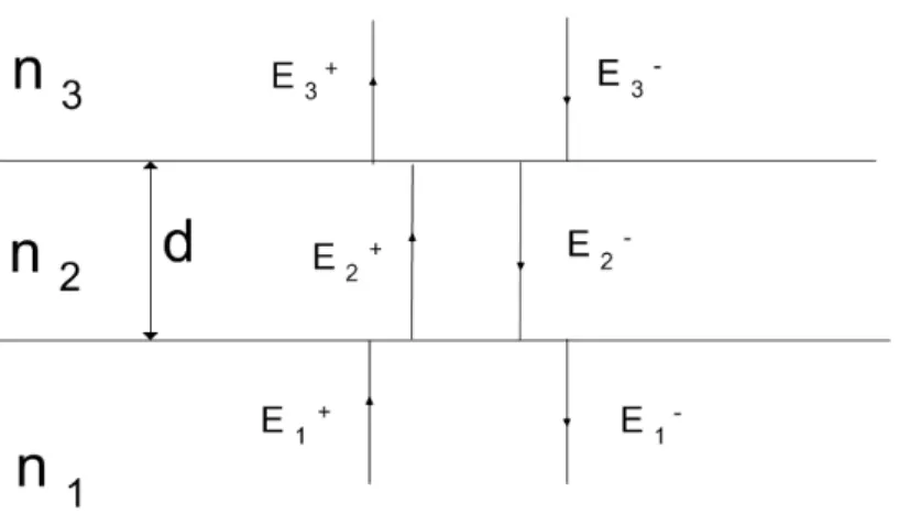
Spectral response of a Bragg grating can be calculated with Transfer Matrix Method (TMM) [30]. Surface corrugation introduces an effective index change and the grating structure can be modelled as a multilayered periodic structure. Figure 2. 8 represents a grating and its multilayered model. First, we study transmission and reflection from a single interface and we get a matrix relationship between the electric fields of the two medium. Then we will extend this concept to the periodic structure by multiplying the matrices for each layer. Figure 2. 9 shows a thin film with thickness of d and refractive index of n2. The electric
fields for three layers are written as
E = ˆ yE+ 1 e−jk1x+ ˆyE1−ejk1x x > 0 ˆ yE+ 2 e−jk2x+ ˆyE2−ejk2x 0 < x < d ˆ yE+ 3 ejk3de−jk3x+ ˆyE3−e−jk3dejk3x x > d (2. 31)
where ki = ω/c = k0ni i = 1, 2, 3 and n1, n2, n3 are the refractive index of each
layer. And we can write magnetic field as
~ H = 1
Figure 2. 8: Waveguide Bragg grating and its layer modelling
Figure 2. 9: Electric field for three layers with different refractive index using the continuity of tangential electric and magnetic field components at the boundary,
E+
n1(E1+− E1−) = n2(E2+− E2−)
If we introduce matrix notation E + 1 E− 1 = S1 E + 2 E+ 2 = 1 t1 1 r1 r1 1 E + 2 E− 2 (2. 34)
here r1and t1are the reflection and transmission amplitudes. They can be written
as r1 = n1− n2 n1+ n2 (2. 35) t1 = 2n1 n1+ n2 (2. 36) we can write the same equations for the second interface with an extra phase term and E + 2 E− 2 = S2 E + 3 E+ 3 = 1 t1 ejδ2 r2ejδ2 r2e−jδ2 e−jδ2 E + 3 E− 3 (2. 37)
phase term is δ2 = k2d = k0n2d2. We define the ratio of the E3+ and E11 to the
E1+ as t = E3+
E1+ and r = E−1 E+1 . E
−
1 is the amplitude of reflected light and E3+ is the
amplitude of transmitted light. Transfer matrix can be written as S = a b c d and we get r = c a and t = 1
a. Transmission and reflection of the layer are the
ratio of the transmitted power and reflected power to the incident power which is the square of electric field and
T = n3 n1
|t|2 (2. 38)
R = |r|2 (2. 39)
It is obvious that if there is no absorbtion R + T = 1 should be satisfied. Matrix method can be extended to multilayered structures. The aim is to find the total transfer matrix by multiplying the transfer matrices for each layer
ST otal = N
Y
i=0
Si (2. 40)
and transmission of multilayered structure is obtained. This method is very suitable to calculate the spectral response of the Bragg grating.
Mach-Zehnder Interferometers
In this chapter we will discuss the use of Mach-Zehnder interferometer (MZI) as a displacement sensor for scanning force microscope. Mach-Zehnder interferometer is integrated on a cantilever and this provides integrated optical interferometric displacement detection. In Section 3.1 theoretical basis and operational principles of MZI will be discussed. In Section 3.2 integration of the MZI with a cantilever will be discussed, transmission characteristics of MZI will be studied. In Section 3.3 waveguide design considerations will be given. In Section 3.4 sensitivity analysis of the sensor will be given. In Section 3.5 basic experimental setup will be proposed.
Figure 3. 1: Schematics of Mach-Zehnder interferometer
3.1
Physical Considerations
Mach-Zehnder interferometer (MZI) is one of the most commonly used integrated optical devices in sensor applications. MZI is based on the interference of two coherent beams. For a waveguide structure, guided light is split into two single mode waveguides by a 3-dB Y junction. Split beams travel different paths and then recombine at an other Y-junction. If the optical path lengths of the two arms differ, there exist a phase difference between the two guided beams and when they recombine, they interfere and the intensity of the light at the output port will change as a function of the phase shift and given as
Iout = I0
2(1 + cos(Φ)) (3. 1)
where I0 is the input intensity and Φ is the phase shift between the two arms.
When the phase shift is equal to π, the two beams interfere destructively and the output will be zero. Figure 3. 1 illustrate the MZI. For sensor applications one of the arms is used as a sensing arm and external physical value introduces optical path difference on the sensing arm leading to interference. For a pressure sensor, sensing arm is located on a suspended diaphragm. When the diaphragm is subject to an applied pressure, the diaphragm deflects and two simultaneous effects introduce phase shift on the sensing arm. The first effect is the photo-elastic effect, which changes the refractive index of the waveguide and the second
0.0 0.2 0.4 0.6 0.8 1.0 π/2 Iou t
Phase Shift (rad)
Figure 3. 2: Output intensity of Mach-Zehnder interferometer as a function of the phase shift. Small variation of the phase shift results in the output intensity variation, at the quadrature point (Φ = π/2) maximum variation can be achieved is the extension of the path length. The phase shift can be written by adding the two contributions as follows;
Φ = β∆L +
Z
LδβdL (3. 2)
here β is the propagation constant of the single mode waveguide and it can be written as β = nef f2πλ , nef f is the effective index of the waveguide, ∆L is the
path elongation and δβ is the change of the propagation constant due to the photo-elastic effect. Fig. 3. 2 shows the output intensity variation as a function of the phase shift between the two arms. The sensitivity of the interferometer is defined as the output intensity variation per unit physical value such as pressure.
dIout I0dP
= sin ΦdΦ
dP (3. 3)
where P is the applied applied physical value. Two things should be noted for Fig. 3. 2. First there is a very linear region between Φ = π/3 and Φ = 2π/3, secondly
this region has the steepest slope. Clearly, the maximum sensitivity occurs in this region with Φ = π
2 where the slope of the output intensity is maximum and
it is called quadrature point. In order to increase sensitivity MZI must be biased to quadrature point by introducing π/2 phase shift.
3.2
Mach-Zehnder Interferometer as a
Dis-placement Sensor
The operational principle of the displacement sensor is simple, a single mode waveguide is divided into two arms with a Y-junction and one of the arm is placed on the cantilever and the other arm is placed on fixed side of the substrate and these two arms are combined with another Y-junction. Fig. 3. 3 represents the top view of the MZI integrated on the cantilever. As the the cantilever displaces, a phase shift is produced between the the two arms and the two beams interfere. As stated before, we can write the phase shift as
Φ = β∆L + Z LδβdL = β∆L + Z L∆nef f 2π λ dL (3. 4)
here there are two contributions; photo-elastic effect and path elongation. They can be additive or subtractive. If the cantilever bends in negative z direction optical path of the waveguide on the upper surface of the cantilever increases (∆L > 0) and stress is positive (tensile). On the other hand, change of refractive index under the tensile stress will be negative or positive depending on the value of the stress optic coefficient of the cantilever. Longitudinal stress optic coefficient for GaAs is positive. This means, under the tensile stress refractive index increases. For SiO2, Si3N4 and Si longitudinal stress optic coefficient is
negative and refractive index decreases under tensile stress. As a result GaAs is the most suitable material for our purpose. Other materials may also be possible with varying sensitivities. As stated before, longitudinal stress is dominant and it decreases linearly along the cantilever and we can write
σ(x) = σmax
(Lcan− x)
Lcan
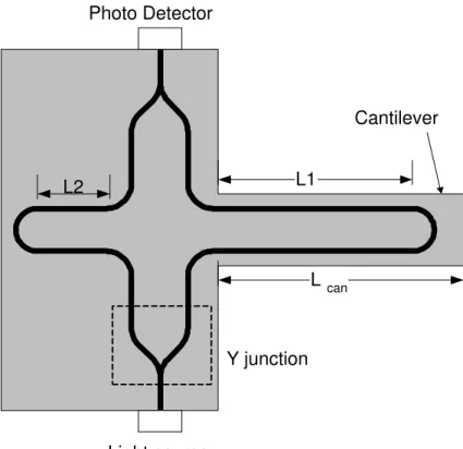
Y junction Photo Detector Light source L can L1 L2 Cantilever
Figure 3. 3: Schematic of Mach-Zehnder interferometer integrated on a cantilever.
where Lcan is the cantilever length and x is the distance from the supporting
point. Using photo-elastic effect, index change can be written as ∆nef f = CTσmax(Lcan− x)
Lcan (3. 6)
Using FEM, we can calculate the stress distribution and the path elongation on the cantilever. Also an analytical expression can be written for maximum stress and inserting into Eq. 3. 4 we get
Φ = β∆L + 4πCTσmax λ Z LM ZI 0 (Lcan− x) Lcan dL (3. 7)
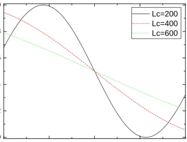
-2 -1 0 1 2 0.0 0.2 0.4 0.6 0.8 1.0 N o rm a lize d o u tp u t in te n si ty Cantilever displacement (µm) Lc=200 Lc=400 Lc=600
Figure 3. 4: Output intensity of Mach-Zehnder interferometer as a function of the cantilever displacement for three different cantilever lengths. The interferometer is unbalanced by changing the path length of the two arm in order to achieve steepest slope at z = 0
where LMZI is the length of the MZI and CT is the transverse stress optic
coefficient. Using σmax we get phase difference between the two arms as,
Φ = 2πnef f λ ∆L + 4πCT λ 3Et 2L3 can z Z LM ZI 0 (Lcan− x)dL (3. 8)
∆L is the path elongation and it was calculated using FEM for a GaAs cantilever with length of 200 µm and thickness of 5 µm, ∆L = 0.019 z where z is the displacement of the cantilever. ∆L is proportional with thickness and inversely proportional with length of the cantilever. From Eq. 3. 8 it is seen that the phase difference is a linear function of the displacement of the tip (z ). As the cantilever displaces, the output intensity of the interferometer changes. Fig. 3. 4 shows the output intensity as a function of the cantilever displacement for different cantilever lengths. It is seen that, output intensity is linear about z = 0.
Figure 3. 5: Waveguide structure for Mach-Zehnder interferometer w = 1µm and
H = 0.75µm
order to get maximum sensitivity, the phase shift can be biased by changing the length of the two arms. For maximum sensitivity L1− L2 = 8nλef f is chosen.
3.3
Waveguide Design
Waveguide design is the central part of the interferometer. The interferometer can be divided into two parts; Y-junction and the curved waveguide on the cantilever. The waveguide must be single mode. Multimode waveguide decreases the visibility of the interferometer which also decreases the sensitivity. High index contrast must be chosen in order to decrease bending losses.
Fig. 3. 5 shows the single mode waveguide structure for w = 1 µm and H = 0.75 µm. Stress reaches its maximum value at the surface and to get homogenous stress H must be small compared to the cantilever thickness. Bending losses are another important design consideration. Fundamental limitation is the bending of the waveguide on the cantilever with radius of less than 25 µm. Above waveguide
Figure 3. 6: Y junction
structure provides bending loss of less than 10 dB for R > 9µm radius. Another important design consideration is the Y-junction. We choose a standard s-bend Y junction, the angle of the junction must be less than 1 degree in order to support adiabatic transition of the mode. For this structure, radiation loss is negligible due to the high index contrast. Fig. 3. 6 shows a typical Y junction where the radius of curvature is about 50000 µm and distance d is 50 µm. The input straight waveguide must be long enough to eliminate the radiative modes before the Y-junction.
3.4
Sensitivity Analysis
Sensitivity of the microscope is one of the parameters that defines the performance of the microscope. The resolution of a scanning microscope is directly related to the sensitivity and the noise of the system. Sensitivity is defined as the normalized output intensity variation per unit displacement of the cantilever and it can be written as
Sd=
∆I
I0∆z
(3. 9) here ∆I is the output intensity variation and ∆z is the displacement of the cantilever. This sensitivity is called displacement sensitivity and we can also
Lcan(µm) 200 500 500 1000
LM ZI(µm) 150 150 300 700
Sd(˚A−1) 6.9 10−5 2.0 10−5 2.6 10−5 1.4 10−5
Table 3.1: Calculated displacement sensitivities.
define force sensitivity as the output intensity variation per unit force applied on the cantilever such as,
Sf =
∆I
I0∆F
(3. 10) Sensitivity can be calculated by taking the derivative of the output intensity as a function of the cantilever displacement. The important thing that has to be considered is that, the microscope must work at the most sensitive region where the slope is maximum. It should also mentioned that if we bias the phase difference by adjusting the path lengths, linear output can be achieved over a longer range ( ∼ 1 µm) which means constant sensitivity. The calculated displacement sensitivities are summarized in Table 3.1.
3.5
Experimental Setup
Experimental setup for this method is simple. It requires a light source and a photodetector. Another advantage of the MZI is that it is a broad band interferometer. The output intensity does not change due to the wavelength variation of the light source. Intensity variation of light source is the main noise source of the system. To eliminate the intensity variation a directional coupler can be used with a differential amplifier.
Bragg Gratings
In this chapter a Bragg grating (BG) will be introduced as a displacement sensor for scanning force microscopes. BG is placed on the cantilever near the supporting point and as the cantilever displaces the generated stress changes the reflection spectrum of the BG. Using a narrow band light source it is possible to detect the displacement directly from the intensity modulation. In Section 4.1 basic operational principles will be discussed. In Section 4.2 cantilever design consideration will be given. In Section 4.3 design of Bragg Grating will be discussed.
4.1
Operation Principles
Bragg gratings (BG) are extensively used as a wavelength selective elements in optical devices. A BG is formed by creating a periodic corrugation or refractive index modulation in optical waveguides or fibers. BGs are useful because of their frequency dependent reflection spectrum. They are, in general, characterized by a central wavelength and the bandwidth of the reflection band. These structures can be thought of as one dimensional diffraction gratings which diffract light from a forward travelling mode into a backward travelling mode. From the well known Bragg condition, the central wavelength of the grating can be written as
λB = m2nef fΛ (4. 1)
where nef f is the effective index of the structure and Λ is the period of the grating
and m is an integer number. The bandwidth of BG, ∆ν, is proportional to the effective index modulation ∆nef f and is approximately given by
∆ν
ν =
∆n
nef f
(4. 2) The effect of the grating on the propagation of light in the waveguide can be modelled using coupled-mode theory (CMT). CMT [26] predicts that the peak reflectivity of a BG is given by
Rmax = tanh2(κL) (4. 3)
where L is the grating length and κ is the grating strength (coupling coefficient). Waveguide Bragg gratings can be formed by physically corrugating the waveguide surfaces as is done in DFB lasers. Reflection spectrum of BG depends on the effective index of the waveguide, any variations of the refractive index result in change of reflection spectrum. Therefore, Bragg gratings have been applied to sense a number of physical values including strain [32], temperature [33] and magnetic fields [34]. These applications are based on the same principle, i.e: measurement of Bragg wavelength shift caused by external effects. In all these methods, a broad band optical source such as a LED, or a superfluorescent device
is used as the light source. To measure the shift in wavelength, external spectrum analyzers are employed. Recently many signal-processing methods are developed to directly measure the intensity modulation of the reflected light [35]. In one method, a light source with a very narrow spectral width such as DFB laser, is used in conjunction with a BG. Typically a BG has much larger spectral width (0.5 nm) than a DFB laser (∼ 1 pm). If the laser wavelength coincides within the reflection spectrum of the BG, the reflected light associated with the laser can be detected at the output. The output intensity at the detector is proportional to the overlap integral of the function f (λ − λL) and g(λ − λg) representing the
spectral characteristics of the laser and BG, respectively [35]. Assuming these functions as Gaussians, we can write,
f (λ − λL) = P0 2 ∆λL s ln2 π exp[−4ln2( λ − λL ∆λL )2] (4. 4) g(λ − λg) = Rexp[−4ln2( λ − λg ∆λg )2] (4. 5)
where ∆λL and ∆λg are the spectral widths and λL and λg are the central
wavelengths of laser and grating, respectively and P0 is the total power of the
laser and R is the reflectivity of the grating. The overlap integral can be written as
Iout =
Z ∞
0 f (λ − λL)g(λ − λg)dλ (4. 6)
Since spectral width of BG, ∆λg, is much larger than that of the laser, ∆λL, Iout
is Iout ' P0g(λL− λg) (4. 7) Iout = P0Rexp[−4ln2( ∆λc ∆λg )2] (4. 8) where ∆λc= λL− λg (4. 9)
Defining Bragg wavelength as;
we can write,
Iout = P0Rexp[−4ln2(
λL− 2nefΛ
∆λg
)2] (4. 11)
From Eq. 4. 11 it is clearly seen that output intensity depends on the effective index of the grating. Any changes in effective index of the grating due to external effects, modulates the output intensity. From this modulation, it is possible to determine the external physical quantity. The most sensitive operation can be achieved by tuning the laser wavelength such that ∆λc= ∆λg/2 where the slope
of reflection onset is maximum. Among the advantages of this method are that, it does not require any spectrum analyzer or a filter, it is optical and integrated. It should also be mentioned that Ioutstrongly depends on the reflection spectrum.
Narrow band-width provides higher intensity variation with small index change.
4.2
Cantilever Design
In any cantilever design , the measurement of the displacement of the cantilever with high sensitivity is the essential task. The design of the cantilever and the type of the integrated sensor plays a fundamental role to increase the sensitivity. Perviously, much work have been done to enhance the sensitivity of AFM [36]. Bending of the cantilever generates stress which is the necessary physical quantity used to characterize the displacement of the cantilever. Figure 4. 1 shows the
Fiber
Figure 4. 1: Schematics of cantilever integrated with a Bragg grating. schematics of the cantilever integrated with a Bragg grating. Bragg grating is loaded on the supporting point of the cantilever. Photo-elastic effect is used for