Formation of quantum structures on a single nanotube by modulating hydrogen adsorption
O. Gu¨lseren,1T. Yildirim,2and S. Ciraci11
Department of Physics, Bilkent University, Ankara 06800, Turkey
2NIST Center for Neutron Research, National Institute of Standards and Technology, Gaithersburg, Maryland 20899, USA 共Received 17 October 2002; revised manuscript received 2 June 2003; published 18 September 2003兲
Using first-principles density functional calculations we showed that quantum structures can be generated on a single carbon nanotube by modulating the adsorption of hydrogen atoms. The band gap of the hydrogen-free zone of the tube widens in the adjacent hydrogen covered zone. The sudden variation of the band gap leads to band offsets at the conduction- and valence-band edges. At the end, the band gap of the whole system is modulated along the axis of the tube, which generates quantum wells or quantum dots. Specific electronic states are confined in these quantum wells. The type and radius of the nanotube and the extent and sequence of hydrogen-free and hydrogen-covered zones can provide several options to design a desired optoelectronic nanodevice.
DOI: 10.1103/PhysRevB.68.115419 PACS number共s兲: 73.22.⫺f, 73.40.Lq, 61.48.⫹c, 73.20.Hb
I. INTRODUCTION
Novel properties and fundamental effects of electrons have been revealed in lower-dimensional quantum structures, such as multiple quantum wells, quantum dots, etc. During last two decades several new electronic devices have been developed from these quantum structures.1Fabricating even smaller and more efficient devices is now the prime drive towards nanotechnology and molecular electronics. One of the grand challenges of research on carbon nanotubes2 has been the realization of nanometer optoelectronic devices. To this end single-wall carbon nanotubes 共SWNT’s兲 have been explored actively with the motivation of finding a new de-vice application.3–7In particular, important effects of the ad-sorption of foreign atoms共i.e., functionalization兲 on the elec-tronic properties have been observed. Remarkable changes in the electrical resistance and thermoelectric power of a SWNT upon exposure to gaseous molecules such as NO2, NH3, and O2 have been exploited to form chemical sensors.3,4
In this paper we present a quantum well structure gener-ated by the modulating adsorption of hydrogen atoms on a semiconducting SWNT. It is known that a SWNT can be either a metal or a semiconductor depending on its chiral vector and radius, but may become a semiconductor even with a larger band gap, when it is exohydrogenated.8,9 Hence, our idea of forming quantum structures on a SWNT exploits this important effect of hydrogenation. Electrons or holes can be confined in a hydrogen-free region of SWNT’s sandwiched between two regions, which are uniformly hy-drogenated.
II. MODEL AND METHOD OF CALCULATION
These findings are obtained from extensive state-of-the-art, first-principle density functional calculations10within the generalized gradient approximation11 for fully optimized atomic positions as well as the lattice constant. The predic-tive power of the density functional theory was proved in earlier studies related to the atomic structure, energetics, and electronic structure of various carbon nanotubes.8,9,12 We
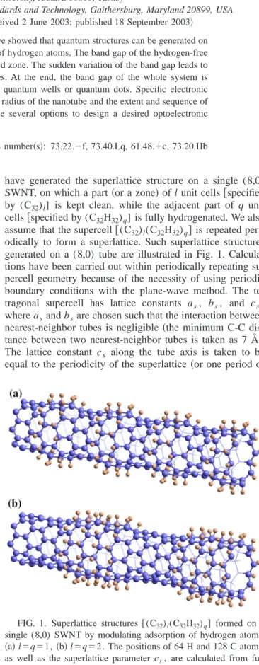
have generated the superlattice structure on a single (8,0) SWNT, on which a part共or a zone兲 of l unit cells 关specified by (C32)l] is kept clean, while the adjacent part of q unit cells关specified by (C32H32)q] is fully hydrogenated. We also assume that the supercell关(C32)l(C32H32)q兴 is repeated peri-odically to form a superlattice. Such superlattice structures generated on a (8,0) tube are illustrated in Fig. 1. Calcula-tions have been carried out within periodically repeating su-percell geometry because of the necessity of using periodic boundary conditions with the plane-wave method. The te-tragonal supercell has lattice constants as, bs, and cs, where asand bsare chosen such that the interaction between nearest-neighbor tubes is negligible 共the minimum C-C dis-tance between two nearest-neighbor tubes is taken as 7 Å兲. The lattice constant cs along the tube axis is taken to be equal to the periodicity of the superlattice共or one period of
FIG. 1. Superlattice structures 关(C32)l(C32H32)q兴 formed on a
single (8,0) SWNT by modulating adsorption of hydrogen atoms. 共a兲 l⫽q⫽1, 共b兲 l⫽q⫽2. The positions of 64 H and 128 C atoms, as well as the superlattice parameter cs, are calculated from full
using ultrasoft pseudopotentials for carbon atoms,13the total energy converges within 0.5 meV/atom. Owing to the very large lattice constants of the supercell, k-point sampling is done only along the tube axis by using the Monkhorst-Pack special k-point scheme14 with 0.02 Å⫺1 k-point spacing.
Fully relaxed geometries are obtained by optimizing all atomic positions 共as many as 96 for l⫽q⫽1 and 192 for l
⫽q⫽2) and the lattice constant 共or superlattice parameter兲
csalong the tube axis until the maximum force and stress are less than 0.01 eV/Å and 0.1 GPa, respectively. Using the atomic structure determined from the optimization of the su-perlattice, l⫽q⫽2, in particular those of the atomic posi-tions at the interface between hydrogenated and bare SWNT, we studied superlattices having larger lattice parameter. This way, we were able to treat relatively longer periodic quantum structures including large numbers of atoms共i.e., 120 C and 64 H atoms corresponding to l⫽3, q⫽2 and also 120 C and 96 H atoms corresponding to l⫽2, q⫽3, with cs⬃5c) without further structure optimization. Hence, we have stud-ied four different superlattices with different periodicities, i.e., l⫹q⫽2, 4, and 5.
III. FORMATION OF QUANTUM STRUCTURES BY BAND-GAP MODULATION
First we demonstrate how the electronic structure is modulated periodically in direct space so that a multiple-quantum-well structure共MQWS兲 is generated on a prototype zigzag (8,0) SWNT. The bare (8,0) SWNT is a semiconduc-tor with a direct band gap, Eg0⫽0.64 eV. Unsaturated * states of carbons are active sites for the adsorption of hydro-gen atoms. A single hydrohydro-gen atom is adsorbed on top of each carbon and completes the fourth covalent bond. The adsorption changes the planar s p2bonding on the cylindrical surface to a local s p3-like bonding. The resulting structure is stable by an energy gain of 2.5 eV. This binding energy is relatively higher than the binding energy of H on the graphene due to curvature effects.12,15Owing to the coupling between nearest-neighbor H atoms, saturation of all carbon atoms with hydrogens appears to be even more stable with an average binding energy Eb⬃2.7 eV/atom. Exohydrogena-tion共i.e., saturation of all C atoms of a SWNT externally by H atom兲 gives rise to remarkable effects on the atomic and electronic structure. For example the C-C bonds are length-ened, bond angles change, and the radius of the tube expands by 16%. More importantly, the band gap of the bare (8,0) tube increases from Eg0⫽0.64 eV to EgH⫽2.1 eV. More-over, it is found that the conductance is sensitive to hydrogen adsorption.16,17
conducting 共8,0兲 SWNT a semimetal, the 共9,0兲 tube 共which normally has a very small band gap兲 becomes a semiconduc-tor with a large band gap.
Based on the above discussion, the zone of the SWNT which is kept clean and the zone which is hydrogenated are expected to have different band structure. This is the most crucial aspect that we have to explore. Normally, in the band continua, states in (C32)l 共i.e., specified by l) zone are ex-tended to the adjacent (C32H32)q 共i.e., specified by q) zone. These are propagating 共itinerant兲 states and have com-parable integrated probability 共or charge density兲, in both adjacent zones. Defining l⫽兰l兩⌿n,k(r)兩2dr and q
⫽兰q兩⌿n,k(r)兩2dr, l⬃q for propagating states. On the other hand, if the energy of a state in one 共say, in the hydrogen-free l) zone of the superlattice coincides with the band gap of the adjacent共hydrogenated q) zone, this particu-lar state cannot propagate and has to be confined to the zone it belongs to. Accordingly,lⰇqare very much different. In the past, these confined states have played a central role in optoelectronic device applications of MQWS’s based on semiconductor superlattices such as GaAs-AlGaAs.1At this point, the following three questions have to be addressed before we conclude whether MQWS’s can be realized from the above superlattice structure: 共i兲 Does the hydrogenated region persist or else adsorbed hydrogens can diffuse away to degrade the superlattice structure?共ii兲 What should be the extent of the zones (C32)l and (C32H32)q in order their elec-tronic structure and hence their band gaps to be distinguish-able from each other? 共iii兲 How are the bands aligned, and hence how is the energy band diagram modulated along the nanotube?
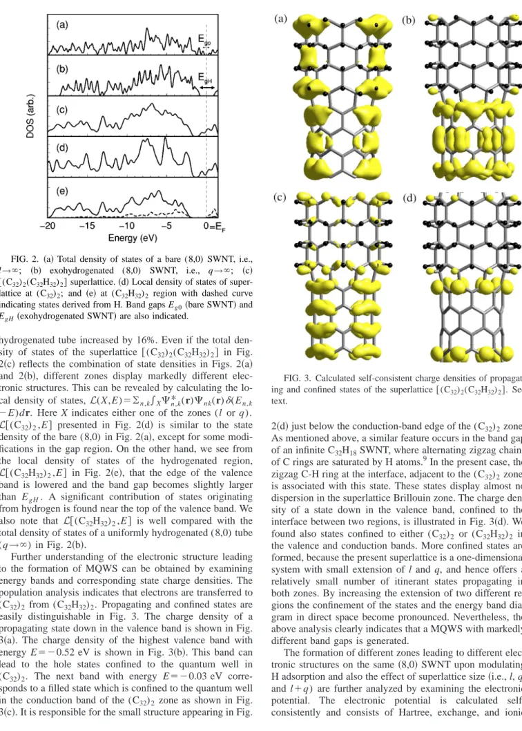
Starting from the first question, we found that the fully hydrogenated zone (C32H32)q is stable, since H atoms re-mained bound to the carbon atoms at the end of full structure optimization. Our static calculation at T⫽0 K did not yield diffusion of H towards the neighboring (C32)l regions. For the second question, the analysis of the charge density for various states suggests that indeed two different electronic structures can be realized in l and q zones of SWNT’s, which are as short as two unit cells. The differences of the elec-tronic structure become pronounced when the extension of (C32)l and (C32H32)q becomes longer. It is, therefore, con-cluded that an (8,0) SWNT as short as a few nanometers is sufficient to make an electronic device. Our arguments are better clarified by the calculated total and local density of states in Fig. 2. Comparison of Figs. 2共a兲 and 2共b兲 shows how the band gap of a bare (8,0) SWNT becomes wider as a result of exohydrogenation. The width of the valence band decreases by⬃2.5 eV, because the radius of the underlying
hydrogenated tube increased by 16%. Even if the total den-sity of states of the superlattice 关(C32)2(C32H32)2兴 in Fig. 2共c兲 reflects the combination of state densities in Figs. 2共a兲 and 2共b兲, different zones display markedly different elec-tronic structures. This can be revealed by calculating the lo-cal density of states, L(X,E)⫽兺n,k兰X⌿n,k* (r)⌿nk(r)␦(En,k
⫺E)dr. Here X indicates either one of the zones (l or q). L关(C32)2,E兴 presented in Fig. 2共d兲 is similar to the state density of the bare (8,0) in Fig. 2共a兲, except for some modi-fications in the gap region. On the other hand, we see from the local density of states of the hydrogenated region,
L关(C32H32)2,E兴 in Fig. 2共e兲, that the edge of the valence band is lowered and the band gap becomes slightly larger than EgH. A significant contribution of states originating from hydrogen is found near the top of the valence band. We also note that L关(C32H32)2,E兴 is well compared with the total density of states of a uniformly hydrogenated (8,0) tube (q→⬁) in Fig. 2共b兲.
Further understanding of the electronic structure leading to the formation of MQWS can be obtained by examining energy bands and corresponding state charge densities. The population analysis indicates that electrons are transferred to (C32)2 from (C32H32)2. Propagating and confined states are easily distinguishable in Fig. 3. The charge density of a propagating state down in the valence band is shown in Fig. 3共a兲. The charge density of the highest valence band with energy E⫽⫺0.52 eV is shown in Fig. 3共b兲. This band can lead to the hole states confined to the quantum well in (C32)2. The next band with energy E⫽⫺0.03 eV corre-sponds to a filled state which is confined to the quantum well in the conduction band of the (C32)2 zone as shown in Fig. 3共c兲. It is responsible for the small structure appearing in Fig.
2共d兲 just below the conduction-band edge of the (C32)2zone. As mentioned above, a similar feature occurs in the band gap of an infinite C32H18SWNT, where alternating zigzag chains of C rings are saturated by H atoms.9In the present case, the zigzag C-H ring at the interface, adjacent to the (C32)2 zone, is associated with this state. These states display almost no dispersion in the superlattice Brillouin zone. The charge den-sity of a state down in the valence band, confined to the interface between two regions, is illustrated in Fig. 3共d兲. We found also states confined to either (C32)2 or (C32H32)2 in the valence and conduction bands. More confined states are formed, because the present superlattice is a one-dimensional system with small extension of l and q, and hence offers a relatively small number of itinerant states propagating in both zones. By increasing the extension of two different re-gions the confinement of the states and the energy band dia-gram in direct space become pronounced. Nevertheless, the above analysis clearly indicates that a MQWS with markedly different band gaps is generated.
The formation of different zones leading to different elec-tronic structures on the same 共8,0兲 SWNT upon modulating H adsorption and also the effect of superlattice size共i.e., l, q, and l⫹q) are further analyzed by examining the electronic potential. The electronic potential is calculated self-consistently and consists of Hartree, exchange, and ionic FIG. 2. 共a兲 Total density of states of a bare (8,0) SWNT, i.e.,
l→⬁; 共b兲 exohydrogenated (8,0) SWNT, i.e., q→⬁; 共c兲
关(C32)2(C32H32)2兴 superlattice. 共d兲 Local density of states of super-lattice at (C32)2; and 共e兲 at (C32H32)2 region with dashed curve indicating states derived from H. Band gaps Eg0共bare SWNT兲 and EgH共exohydrogenated SWNT兲 are also indicated.
FIG. 3. Calculated self-consistent charge densities of propagat-ing and confined states of the superlattice 关(C32)2(C32H32)2兴. See text.
pseudopotentials, Ve(r)⫽VH(r)⫹Vx(r)⫹Vion(r). In Fig. 4 we present the planarly averaged electronic potential
V ¯ e共z兲⫽ 1 asbs
冕
Ve共x,y,z兲dxdy 共1兲and running average of the planarly averaged potential V
¯
r,e(z). Here z is parallel to the axis of SWNT, and in pla-narly averaging the integral is evaluated on the xy plane in the supercell. The running average is the average of V¯e(z) between z⫽zi and z⫽zi⫹z0, z0 being an appropriate sub-periodicity in the cell, such as the peak-to-peak distance of V
¯e(z). As seen in Fig. 4共a兲, the short periodicity l⫽q⫽1 is not sufficient to induce two adjacent zones with markedly different electronic structures. The zone corresponding to exohydrogenated SWNT’s is mixed with the interface region shown by a small peak, and the potential difference between two zones,⌬V, is not too large. In Fig. 4共b兲 the differences between two zones become pronounced, and ⌬V increases for the superlattice, l⫽q⫽2. Figures 4共c兲 and 4共d兲 indicate that the potential V¯r,e(z) becomes flatter as l and q increase from 2 to 3, and two adjacent zones display markedly differ-ent electronic structure. Increasing flattening of V¯r,e(z) with increasing l and q justifies our argument that the formation of quantum structures becomes pronounced for large superlat-tice periodicity. We calculated V¯r,e共1.0 eV, ⫺0.7 eV), 共1.56 eV, ⫺1.08 eV), 共1.37 eV, ⫺1.61 eV), and 共1.75 eV,
⫺0.94 eV) for the superlattices (l⫽1, q⫽1), (l⫽2, q ⫽2), (l⫽3, q⫽2), and (l⫽2, q⫽3), respectively.
Conse-quently, for the same superlattices⌬V is found to be 1.7 eV, 2.64 eV, 2.98 eV, and 2.69 eV. The charge transfer from the
ture and charge transfer at the interface and, also, resulting in the modification of the electronic potential. Experimental and theoretical methods have been proposed in the past to determine the band offsets and, hence, to obtain a band dia-gram perpetuating along the semiconductor heterostructures. A solution of this problem18 involves the following steps: First, the average electronic potentials corresponding to V
¯
r,e(z) for finite l and q, as well as for infinite (C32)l⫽⬁and (C32H32)q⫽⬁, are calculated. The actual atomic positions, especially those at the interface, and the charge transfer be-tween regions are of crucial importance for the band offsets and are incorporated self-consistently in the calculated aver-age electronic potential. Second, for the case of l⫽q⫽⬁ the energy difference between the edge of the valence band EV and average potential—i.e., ⌬EB兩l(q)⫽⬁⫽EV,l(q)⫽⬁
⫺V¯r,e兩l(q)⫽⬁—are calculated. We found ⌬EB for (C32)l⫽⬁ and (C32H32)q⫽⬁to be 2.62 eV and 3.91 eV, respectively. In the third step, one assumes that ⌬EB is unchanged for finite l and q, and determines the valence-band edges of a particu-lar superlattice with given l and q by adding ⌬EB兩l(q)⫽⬁ to the corresponding average potential values V¯r,eof the l and q zones. At the end, the energies of the valence-band edges of two adjacent zones 共i.e., hydrogen free and exohydroge-nated兲 are fixed. Then, the valence-band offset of the super-lattice is⌬EV⫽EV,l⫺EV,q. The energies of the conduction-band edges of the superlattice are determined by adding conduction-band gaps of different zones共calculated for l⫽⬁ and q⫽⬁) to the energies of the valence-band edges, i.e., EC,l⫽EV,l⫹Eg1and EC,q⫽EV,q⫹Eg2. Here, Eg1⫽Eg0 and Eg2⫽EgH in Fig. 2. The conduction-band offset is then determined by subtract-ing these latter energies, i.e.,⌬EC⫽EC,q⫺EC,l.
We note that the above procedure used to determine the band diagram of heterostructures may involve error bars in the short-periodicity superlattices, such as l,q⫽1. In these superlattices V¯r,e(z) is not flat, but exhibits a small variation with z. As seen in Fig. 2, the band gaps in the zones of small l and q can differ from the band gaps calculated for l⫽q
⫽⬁. Moreover, ⌬EB兩l(q) may be different from the corre-sponding values ⌬EB兩l(q). At least, ⌬EB varies with z for small l and q. Since the self-consistent-field 共SCF兲 calcula-tion of large-periodicity superlattices cannot be achieved with the present computational tools and our objective is only to show whether quantum structures can form, we apply the above procedure and use the results of our superlattice calculations to estimate the band offsets. In Fig. 5 we present our estimated values of band offsets for the superlattices (l
⫽q⫽2), (l⫽3; q⫽2), and (l⫽2; q⫽3). The superlattice
(l⫽q⫽1) does not allow us to make any estimation because FIG. 4. Averages of calculated self-consistent electronic
poten-tial of the superlattices. 共a兲 关(C32)1 (C32H32)1], 共b兲 关(C32)2 (C32H32)2], 共c兲 关(C32)3 (C32H32)2], and 共d兲 关(C32)2 (C32H32)3]. Dashed and thick lines are planarly averaged V¯e(z) and running averaged V¯r,e(z), respectively. Relatively higher-cell-averaged po-tential zones correspond to (C32)l. See text.
of the uncertainty in the determination of V¯r,e(z). For (l
⫽q⫽2), ⌬ECand⌬EV⬎0 indicate a type-I 共normal兲 band lineup and give rise to quantum wells in the conduction as well as in the valence band of the (C32)2 zone. This band diagram is consistent with the confinement of states in Figs. 3共b兲 and 3共c兲. It appears that the band gap Eg,l⫽2⬍Eg,l⫽⬁, and the first band with E⫽⫺0.03 eV is confined in the quan-tum well formed in the conduction band of (C32)2 as shown in Fig. 3共c兲. The band lineup of (l⫽3, q⫽2) is type II
共staggered兲, while (l⫽2, q⫽3) displays a normal band
lineup. We note that alternation of band lineups with super-lattice periodicity originates from small values of兩⌬EC兩. For long superlattice periodicity with large l and q it is expected that ⌬EV⬃1.4 eV and EC,l⬃EC,q.
We can check our estimated values by taking a more di-rect and practical approach and deduce the band offsets and resulting energy band diagram from the calculated electronic structure of the superlattice l⫽q⫽2. The energy band dia-gram in direct space is obtained by analyzing the characters and energy positions of the band structure and by examining the gaps of the local density of states shown in Fig. 2. Shifts of the bands corresponding to (C32)2 and (C32H32)2 zones and the resulting band offsets are already incorporated in the local density of states in Figs. 2共d兲 and 2共e兲. The band gaps at the hydrogen-free and exohydrogenated regions of the su-perlattice are different from the values corresponding to l
⫽⬁ and q⫽⬁ and are deduced from the local density of
states to be E ⫽2⬃0.5 eV and E ⫽2⬃2.3 eV,
respec-tively. The band offsets at the valence and conduction band are estimated to be⌬EV⫽⬃1.4 eV and ⌬EC⫽⬃0.4 eV, re-spectively. Keeping in mind that the value of ⌬EC is small and it may be within the error bars in short-periodicity su-perlattices, both procedures are seen to yield similar type of band alignment, i.e., type-I, normal band lineup.
V. DISCUSSION AND CONCLUSIONS
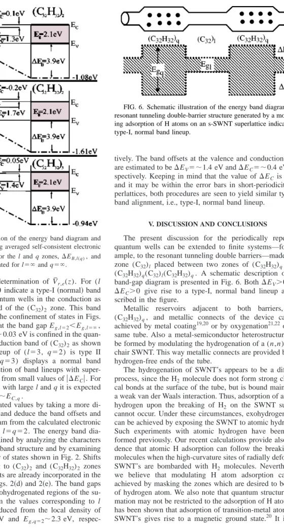
The present discussion for the periodically repeating quantum wells can be extended to finite systems—for ex-ample, to the resonant tunneling double barriers—made by a zone (C32)l placed between two zones of (C32H32)q, i.e., (C32H32)q(C32)l(C32H32)q. A schematic description of the band-gap diagram is presented in Fig. 6. Both ⌬EV⬎0 and
⌬EC⬎0 give rise to a type-I, normal band lineup as de-scribed in the figure.
Metallic reservoirs adjacent to both barriers, i.e., (C32H32)q, and metallic connects of the device can be achieved by metal coating19,20or by oxygenation21,22of the same tube. Also a metal-semiconductor heterostructure can be formed by modulating the hydrogenation of a (n,n) arm-chair SWNT. This way metallic connects are provided by the hydrogen-free ends of the tube.
The hydrogenation of SWNT’s appears to be a difficult process, since the H2 molecule does not form strong chemi-cal bonds at the surface of the tube, but is bound mainly by a weak van der Waals interaction. Thus, adsorption of atomic hydrogen upon the breaking of H2 on the SWNT surface cannot occur. Under these circumstances, exohydrogenation can be achieved by exposing the SWNT to atomic hydrogen. Such experiments with atomic hydrogen have been per-formed previously. Our recent calculations provide also evi-dence that atomic H adsorption can follow the breaking of molecules when the high-curvature sites of radially deformed SWNT’s are bombarded with H2 molecules. Nevertheless, we believe that modulating H atom adsorption can be achieved by masking the zones which are desired to be free of hydrogen atom. We also note that quantum structure for-mation may not be restricted to the adsorption of H atoms. It has been shown that adsorption of transition-metal atoms on SWNT’s gives rise to a magnetic ground state.20 It is ex-FIG. 5. Schematic illustration of the energy band diagram and
band offsets estimated by using averaged self-consistent electronic potentials V¯r,e(z) calculated for the l and q zones, ⌬EB,l(q), and
band gaps Eg1 and Eg2calculated for l⫽⬁ and q⫽⬁.
FIG. 6. Schematic illustration of the energy band diagram of a resonant tunneling double-barrier structure generated by a modulat-ing adsorption of H atoms on an s-SWNT superlattice indicatmodulat-ing a type-I, normal band lineup.
1Highlights in Condensed Matter Physics and Future Prospects, edited by L. Esaki, Vol. 285 of NATO Advanced Study Institute 共Plenum Press, New York, 1991兲.
2S. Iijima, Nature共London兲 354, 56 共1991兲.
3P.G. Collins, A. Zettl, H. Bando, A. Thess, and R.E. Smalley, Science 278, 100共1997兲.
4J. Kong, N.R. Franklin, C. Zhou, M.G. Chapline, S. Peng, K. Cho, and H. Dai, Science 287, 622共2000兲.
5L. Chico, V.H. Crespi, L.X. Benedict, S.G. Louie, and M.L. Co-hen, Phys. Rev. Lett. 76, 971共1996兲.
6A. Bezryadin, A.R.M. Verschueren, S.J. Tans, and C. Dekker, Phys. Rev. Lett. 80, 4036共1998兲.
7V. Derycke, R. Martel, J. Appenzeller, and Ph. Avouris, Phys. Rev. Lett. 80, 2773共2002兲.
8T. Yildirim, O. Gu¨lseren, and S. Ciraci, Phys. Rev. B 64, 075404 共2001兲.
9O. Gu¨lseren, T. Yildirim, and S. Ciraci, Phys. Rev. B 66, 121401 共2002兲.
10M.C. Payne, M.P. Teter, D.C. Allen, T.A. Arias, and J.D. Joan-nopoulos, Rev. Mod. Phys. 64, 1045共1992兲.
11J.P. Perdew, J.A. Chevary, S.H. Vosko, K.A. Jackson, M.R. Ped-erson, D.J. Singh, and C. Fiolhais, Phys. Rev. B 46, 6671
共1992兲.
12O. Gu¨lseren, T. Yildirim, S. Ciraci, and C. Kilic, Phys. Rev. B 65, 155410共2002兲; O. Gu¨lseren, T. Yildirim, and S. Ciraci, ibid. 65, 153405共2002兲.
13D. Vanderbilt, Phys. Rev. B 41, 7892共1990兲.
14H.J. Monkhorst and J.D. Pack, Phys. Rev. B 13, 5188共1976兲. 15O. Gu¨lseren, T. Yildirim, and S. Ciraci, Phys. Rev. Lett. 87,
116802共2001兲.
16A.N. Andriotis, M. Menon, D. Srivastava, and G.E. Froudakis, Phys. Rev. B 64, 193401共2001兲.
17A.N. Andriotis, M. Menon, and D. Srivastava, J. Chem. Phys.
117, 2836共2002兲.
18L. Colombo, R. Resta, and S. Baroni, Phys. Rev. B 44, 5572 共1991兲.
19V.M.K. Bagci, O. Gu¨lseren, T. Yildirim, Z. Gedik, and S. Ciraci, Phys. Rev. B 66, 045409共2002兲.
20E. Durgun, S. Dag, V.M.K. Bagci, O. Gu¨lseren, T. Yildirim, and S. Ciraci, Phys. Rev. B 67, 201401共2003兲.
21P.G. Collins, K. Bradley, M. Ishigami, and A. Zettl, Science 287, 1801共2000兲.
22S. Dag, O. Gu¨lseren, T. Yildirim, and S. Ciraci, Phys. Rev. B 67, 165424共2003兲.