HIGH SPEED AND HIGH EFFICIENCY INFRARED
PHOTODETECTORS
A DISSERTATION
SUBMITTED TO THE DEPARTMENT OF PHYSICS AND THE INSTITUTE OF ENGINEERING AND SCIENCES
OF BİLKENT UNIVERSITY
IN PARTIAL FULFILLMENT OF THE REQUIREMENTS FOR THE DEGREE OF
DOCTOR OF PHILOSOPHY
By
İBRAHİM KİMUKİN
DECEMBER 2004
I certify that I have read this thesis and that in my opinion it is fully adequate, in scope and in quality, as a dissertation for the degree of Doctor of Philosophy.
________________________________________ Prof. Ekmel Özbay (Supervisor)
I certify that I have read this thesis and that in my opinion it is fully adequate, in scope and in quality, as a dissertation for the degree of Doctor of Philosophy.
________________________________________ Asst. Prof. Oğuz Gülseren
I certify that I have read this thesis and that in my opinion it is fully adequate, in scope and in quality, as a dissertation for the degree of Doctor of Philosophy.
________________________________________ Assoc. Prof. Ahmet Oral
I certify that I have read this thesis and that in my opinion it is fully adequate, in scope and in quality, as a dissertation for the degree of Doctor of Philosophy.
________________________________________ Asst. Prof. Özgür Aktaş
I certify that I have read this thesis and that in my opinion it is fully adequate, in scope and in quality, as a dissertation for the degree of Doctor of Philosophy.
________________________________________ Prof. Tayfun Akın
Approved for the Institute of Engineering and Sciences:
________________________________________ Prof. Mehmet Baray,
Abstract
HIGH SPEED AND HIGH EFFICIENCY INFRARED
PHOTODETECTORS
İbrahim Kimukin
Ph. D. in Physics
Supervisor: Prof. Ekmel Özbay
December 2004
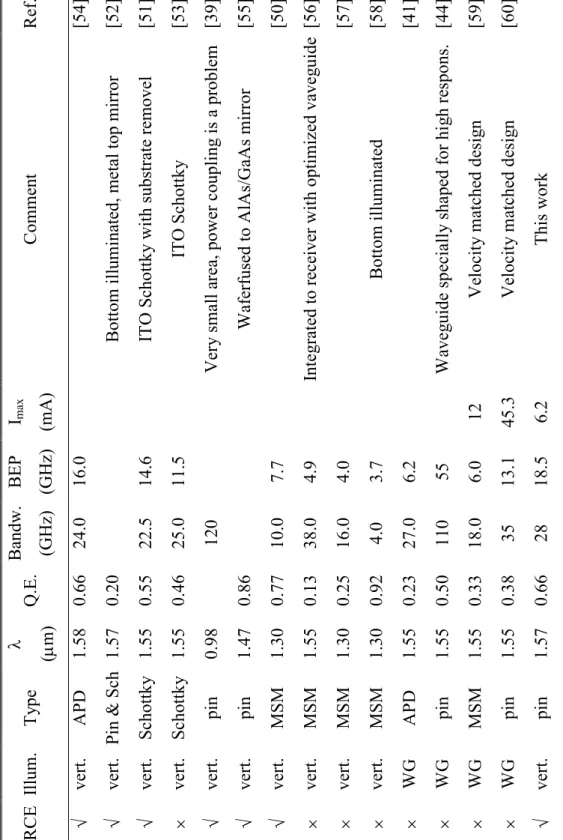
The increasing demand for telecommunication systems resulted in production of high performance components. Photodetectors are essential components of optoelectronic integrated circuits and fiber optic communication systems. We successfully used resonant cavity enhancement technique to improve InGaAs based p-i-n photodetectors. The detectors had 66% peak quantum efficiency at 1572 nm which showed 3 fold increases with respect to similar photodetector without resonant cavity. The detectors had 28 GHz 3-dB bandwidth at the same time. The bandwidth efficiency product for these detectors was 18.5 GHz, which is one of the best results for InGaAs based vertical photodetector.
The interest in high speed photodetectors is not limited to fiber optic networks. In the recent years, data communication through the air has become popular due to
ease of installation and flexibility of these systems. Although the current systems still operate at 840 nm or 1550 nm wavelengths, the advantage of mid-infrared wavelengths will result in the production of high speed lasers and photodetectors. InSb based p-i-n type photodetectors were fabricated and tested for the operation in the mid-infrared (3 to 5 µm) wavelength range. The epitaxial layers were grown on semi-insulating GaAs substrate by molecular beam epitaxy method. The detectors had low dark noise and high differential resistance around zero bias. Also the responsivity measurements showed 49% quantum efficiency. The detectivity was measured as 7.98×109 cm Hz1/2/W for 60 µm diameter detectors.
Finally the high speed measurements showed 8.5 and 6.0 GHz bandwidth for 30 µm and 60 µm diameter detectors, respectively.
Keywords: Photodetector, high speed, high efficiency, resonant cavity enhancement, infrared wavelengths.
Özet
YÜKSEK HIZLI VE YÜKSEK VERİMLİ KIZILÖTESİ
FOTODEDEKTÖRLER
İbrahim Kimukin
Fizik Doktora
Tez Yöneticisi: Prof. Ekmel Özbay
Aralık 2004
Telekomnikasyon sistemlerine ilginin artması yüksek performanslı elemanların üretimiyle sonuçlanmıştır. Fotodedektörler optoelektronik entegre devrelerin ve fiber iletiim sistemlerinin önemli bir parçasıdır. Resonant çınlaç arttırımı tekniğinini InGaAs temelli p-i-n tipi fotodedektörleri geliştirmek için kullandık. Dedektörlerin 1572 nm’deki %66 tepe kuantum verimi rezonatörsüz benzer bir dedektöre göre 3 kat fazladır. Dedektörler aynı zamanda 28 GHz 3-dB bantralığına
sahiptir, ki bu değerler InGaAs temelli düşey fotodedektörler için en iyi sonuçlardan biridir.
Yüksek hızlı fotodedektörlere ilgi sadece fiber optic ağlar ile sınırlı değildir. Yakın zamanda havadan data iletimi kolay kurulum ve değişken yapılarından dolayı populer hale gelmiştir. Hernekadar şu anda kullanılan sistemler 840 nm ve 1550 nm de çalışsa da, orta-kızılötesi dalagaboylarının avantajı yüksek hızlı lazer ve fotodedektörlerin üretimine sebep olacaktır. InSb temelli p-i-n tipi dedektörler orta-kızılötesi dalagaboylarında (3 ten 5 µm’ye) kullanılmak üzere üretilip testedildi. Dedektör katmanları yarı-yalıtkan GaAs altaşın üzerine moleküler ışın demeti metodu ile büyütüldü. Dedektörler sıfır volt civarında düşük karanlık akım ve yüksek dirence sahiptiler. 60 µm çaplı dedektörlerin hassasiyeti 7.98×109 cm
Hz1/2/W olarak ölçüldü. Son olarak yüksek hız ölçümlerine göre 30 µm ve 60 µm çaplı dedektörlerin hızları sırasıyla 8.5 GHz ve 6.0 GHz’tir.
Anahtar Kelimeler: Fotodedektör, yüksek hız, yüksek verim, resonant çınlaç arttırımı, kızılötesi dalgaboyları.
Acknowledgements
It is my pleasure to express my deepest gratitude to my supervisor Prof. Ekmel Özbay for his invaluable guidance, motivation, encouragement, confidence, understanding, and endless support. My graduate study under his supervision was my lifetime experience. It was an honor to work with him, and I learned a lot from his superior academic personality.
I would like to thank Prof. Orhan Aytür and Dr. Tolga Kartaloğlu for their help in high speed measurements in the infrared wavelengths. I would like to thank Prof. Cengiz Beşikçi, Selçuk Özer, and Orkun Cellek for their help in responsivity measurements of InSb photodetectors.
I also thank the members of the thesis committee, Asst. Prof. Oğuz Gülseren, Assoc. Prof. Ahmet Oral, Asst. Prof. Özgür Aktaş, and Prof. Tayfun Akın for their useful comments and suggestions.
I would like to thank all the former and present members of Advanced Research Laboratory for their continuous support. I want to especially thank the group members of the detector research team: Necmi Bıyıklı, Bayram Bütün,
Turgut Tut. It was a pleasure to work with these hard-working guys in the same group. Other special thanks go to Murat Güre and Ergün Kahraman for their technical help and keeping our laboratory in good condition.
Finally I would express my endless thank to my family for their understanding and continuous moral support. Very special thanks belong to my wife, Sevcan, for her endless moral support, understanding, and love.
Contents
Abstract Özet Acknowledgements Contents List of Figures List of Tables 1 Introduction 2 Theoretical Background 2.1 Photodetectors . . . 2.1.1 Photodetector Basics . . . 2.1.2 Photodetector Structures . . . i iii v vi xi xvii 1 5 5 6 10 vii2.1.3 Photodetector Operation . . . 2.2 Resonant Cavity Enhancement . . .
2.2.1 RCE Formulation and Optimization . . . 2.2.2 Standing Wave Effect . . . 2.3 Optical Design . . . 2.3.1 Transfer Matrix Method . . . 2.3.2 Distributed Bragg Reflectors . . .
3 Fabrication and Characterization
3.1 Basic Fabrication Steps . . . 3.1.1 Sample Cleaving . . . 3.1.2 Sample Cleaning . . . 3.1.1 Photolithography . . . 3.1.4 Development . . . 3.1.5 Etch . . . 3.1.6 Metallization . . . 3.1.7 Lift-off . . . 3.1.8 Thermal Annealing . . . 3.1.9 Dielectric Deposition . . . 3.2 Measurement Setups . . . 3.2.1 Reflection and Transmission Measurements . . . 3.2.2 Current Voltage Measurements . . . 3.2.3 Quantum Efficiency Measurements . . . 3.2.4 High Speed Measurements. . .
12 15 15 18 19 19 23 26 26 26 27 28 31 32 35 36 37 38 41 41 42 43 45 viii
4 InGaAs p-i-n Photodetector
4.1 Design . . . 4.2 Fabrication . . . 4.2.1 Large Area Photodetector Fabrication . . . 4.2.2 Small Area Photodetector Fabrication . . . 4.3 Measurements. . .
4.3.1 Current-Voltage Characteristics . . . 4.3.2 Responsivity Characteristics . . . 4.3.3 High-Speed Characteristics . . . 4.4 Conclusion . . .
5 InSb p-i-n Photodetector
5.1 Design . . . 5.2 Fabrication . . . 5.3 Measurements. . . 5.3.1 Current-Voltage Characteristics . . . 5.3.2 Responsivity Characteristics . . . 5.3.3 High Speed Characteristics . . . 5.4 Conclusion . . .
6 Conclusion and Suggestions for Further Research
Bibliography
A Frequency Response Calculation for a Photoetector
B TMM Based Detector Design
47 49 58 60 65 68 70 75 76 79 81 84 85 91 91 95 99 102 106 109 121 122 ix
C List of Publications 126
List of Figures
2.1 2.2 2.3 2.4 2.5 2.6 2.7 2.8 2.9 2.10 2.11 2.12 2.13 3.1 3.2 3.3Energy diagram of a p-i-n photodetector . . . Energy diagram of a Schottky photodetector . . . Cross-section of vertical illuminated photodetectors . . . Cross-section of edge illuminated photodetectors . . . Output current versus time for a constant illumination across the depletion region . . . Small signal equivalent circuit for photodetector . . . Generalized structure of a resonant cavity enhanced photodetector . . . . Electric field amplitudes at the interface . . . The propagation of wave inside the same medium . . . Electric field values before and after the structure . . . Reflection spectrum and phase difference of InP/Air DBR with 3 pairs Reflection spectrum and phase difference of InP/InAlGaAs DBR with 40 pairs . . . Transmission spectrum of Si/SiO2 notch filter centered to 1550 nm . . .
Photographs of some samples with fabricated photodetectors on them Photographs of the masks . . . Plots from the mask file (a) a photodiode with 100 µm diameter active
7 8 11 11 12 13 16 20 21 22 24 24 25 27 28 xi
3.4 3.5 3.6 3.7 3.8 3.9 3.10 3.11 3.12
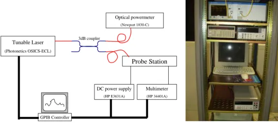
area, (b) development marks used in the p+ ohmic step, (c) p+ ohmic transmission lines and the development marks, and (d) alignment marks . . . Plot of the mask containing large area photodetectors. All the fabrication steps are shown aligned to each other. The mask contains around 115 photodetectors . . . Image-reversal photolithography (after reference [30]) . . . SEM picture wet etch profiles . . . (a) The current flow between the contacts. (b) The schematics of the model used for the ohmic contact characterization. (c) The p+ ohmic transmission line (center) is used for ohmic quality measurements. Also the alignment marks (up) and the development marks (bottom) can be seen . . . Pictures of equipments: (a) mask aligner, (b) surface profilometer, (c) thermal evaporator and RF sputter, (d) PECVD, (e) RIE, (f) RTA . . . . (a) The reflectivity measurement setup. The light source (blue) the fiber probe and the optical spectrum analyzer can be seen. (b) The reflectivity of the InGaAs based photodetector wafer . . . (a) The probe station. With the help of objectives, we can make contact to the pads of the photodetectors. (b) The sample on the probe station, where two DC probes touch the pads, while the active are is illuminated with the fiber . . . HP4142B and the computer control . . . Quantum efficiency measurement setup with the monochromator . . . .
29 30 31 33 38 40 42 43 43 44 xii
3.13 3.14 4.1 4.2 4.3 4.4 4.5 4.6 4.7 4.8 4.9 4.10
Quantum efficiency measurement setup with the tunable laser . . . High Speed measurement setup . . . Lattice parameter vs. energy gap of III-V compounds used with InP and GaAs based devices (after reference [61]) . . . Charge drift velocity as a function of electric filed strength for various semiconductors (after reference [61]) . . . (a) Lattice match conditions of quaternary compounds to InP (after reference [68]). (b) Energy gap of III-V compounds (after reference [69]) . . . Refractive index of (In0.52Al0.48As)χ(In0.53Ga0.47As)1-χ as a function of
wavelength for different values of χ (after reference [70]) . . . Spectral reflectivity of the bottom DBR calculated using TMM . . . The measurement (solid line) and calculation (dotted line) results for a region on the wafer where the shift was %4 . . . The n+ ohmic contacts before (a) and after (b) the RTA . . . The p+ ohmic contacts before the metal deposition (a) and after the RTA . . . (a) The color change on the surface is due to the variation of the etch depth (b) the mesa contour can be seen as a thin black line below the p contact . . . (a) The surface was covered with silicon nitride, and the photograph shows the surface after photolithography, (b) the surface of the sample after the HF etch and the cleaning. Some area on top of the contacts was open, and the sidewalls were covered . . .
45 46 48 52 53 55 56 59 61 62 62 63 xiii
4.11 4.12 4.13 4.14 4.15 4.16 4.17 4.18 4.19 4.20 4.21
(a, b) The photoresist before the metallization, (c, d) interconnect metals after the cleaning . . . SEM images of large area photodetectors . . . Cross-section of the sample (a) after airbridge metallization, and (b) after the liftoff of the metal . . . SEM picture of airbridges . . . 3D illustration of a fabricated photodetector . . . Pictures of small area photodetectors obtained with optical microscope and SEM . . . . . . (a) Current voltage characteristics of a 30 µm diameter photodetector, where the breakdown can be seen around -14 V bias. (b) The logarithmic plot of I-V characteristics of 30, 60, 100, 150, and 200 µm diameter photodetector (from bottom to top respectively) . . . (a) Dark current of photodetectors at 1 V reverse bias as a function of detector area. (b) Dark current density of photodetectors at 1 V reverse bias as a function of detector area. The linear decrease can be seen for detectors having 60 µm diameter . . . (a) Calculated differential resistance of the photodetectors with 30, 60, 100, 150, and 200 µm diameter (from top to bottom respectively). (b) The maximum differential resistance of photodetectors as a function of detector area . . . . . . (a) Calculated differential resistance of the photodetectors at zero bias. (b) R0A product as a function of detector area . . .
(a) The spectral quantum efficiency measurement for successive recess 64 65 67 68 68 69 71 72 73 74 xiv
4.22 4.23 5.1 5.2 5.3 5.4 5.5 5.6 5.7 5.8 5.9 5.10
etches. (b) The measurement and calculation of the spectral quantum efficiency with the peak at 1572 nm . . . (a) The photocurrent vs optical power measurement of the photodetectors under various bias voltages. (b) Log-Log plot of the previous data for 0 and 4 V bias voltages . . . (a) The temporal response of 5×5 µm2 area photodetector under 7 V
reverse bias. (b) The calculated frequency response of the photodetector . . . Spectral transmission of the atmosphere at the sea level . . . Lattice constant and energy gap of semiconductors . . . Details from InSb wet etch . . . Modified mesa isolation step used during the fabrication of InSb photodetectors . . . (a) Cross-section of a fabricated photodetector (b) Photograph of photodetector with 150 µm diameter . . . Current-voltage characteristics and differential resistance of 30 µm diameter photodetector at 300 K (dotted line) and 77 K (solid line) . . . Measured current-voltage characteristics of 60, 100, and 150 µm diameter photodetectors at 77 K . . . (a) Dark current at -0.5 V as a function of area, while (b) shows the dark current density (J0) as a function of area . . .
Calculated differential resistance (Rd) as a function of bias voltage . . .
(a) The zero bias differential resistance (R0) as a function of detector
area. (b) Resistance-area product (R0A) as a function of detector area .
77 78 80 81 85 87 88 90 92 92 93 94 95 xv
5.11 5.12 5.13 5.14 5.15 5.16 5.17 5.18
Responsivity of the photodetectors at 1550 nm as a function of the reverse bias. The inset shows the spectral responsivity measurement under different reverse bias voltages ranging from 0.2 to 0.6 V . . . Spectral simulation results for optical reflection and absorption in the p+ and n- InSb layers . . . Picture of the setup from Electrical Engineering of METU . . . Results of the spectral responsivity measurements are shown for 80 µm (solid line) diameter and 60 µm (dotted line) diameter photodetector . . . (a) The schematic diagram of the optical parametric oscillator, (b) pictures of the experimental setup . . . Temporal response of a 30 µm diameter detector under (a) 0.5V, (b) 1.0V, and (c) 2.5V bias . . . Temporal response of a 60 µm diameter detector under (a) 0.5V, (b) 1.0V, and (c) 2.5V bias . . . Fast Fourier Transform of the temporal responses of the photodetectors. Results for (a) 60 µm diameter and (b) 30 µm diameter photodetectors as a function of bias are shown. (c) 3-dB bandwidth of the 30 and 60 µm diameter photodetectors as a function of applied bias
96 97 98 99 100 103 104 105 xvi
List of Tables
3.1 3.2 3.3 4.1 4.2 4.3 4.4 4.5 5.1 5.2 5.3Etch rates of some recipes used in our processes . . . Etch rates of some recipes used in RIE etch . . . Growth conditions and properties of dielectric films . . . Comparison of this work with the previous research . . . Optical properties of various III-V semiconductor compounds . . . Band discontinuities of some heterostructure systems . . . Epitaxial structure of the InGaAs based pin detector wafer . . . Etch rates of some common etchants. The rates are indicated as nm/sec. Stop means no etch . . . Gases and their absorption properties . . . Properties of some low energy gap semiconductors . . . Epitaxial layers of InSb p-i-n photodetector . . .
33 34 41 50 51 52 57 61 82 83 85 xvii
Chapter 1
Introduction
The invention of the telephone led to an enormous world wide telecommunication network. Especially during and after the Second World War, the demand for the calling services resulted to both cheaper and faster services. The invention of the first solid-state transistor in 1947, and then the integrated circuit opened the age of computing and communication [1]. In 1960's researchers developed the first laser [2].
The development of the first commercially feasible optical fiber in 1970's made the fiber optic communication a promising candidate for telecommunication [3]. In the early 1980's satellites capable of carrying nearly 100,000 simultaneous calls are used for telephone calls. Demand for the faster, cheaper, and less noisy communication made the first transatlantic undersea fiber-optic telephone cable possible that replaced the copper one that had been installed in 1956. That was the first fiber-optic revolution in telecommunication.
The second revolution came with the introduction of wavelength division multiplexing (WDM). Telephone companies has laid cables containing 24 to 36 fibers with 2.5 Gbit/s rate, many had been reserved as “dark fiber”. But the tremendous traffic has crowded these cables that once seemed so
CHAPTER 1. INTRODUCTION 2
voluminous. This demand was due to the growth of the Internet, and the demand for more information transform for entertainment and communication. In the mid 1990's, companies began using systems capable of transmitting at four wavelengths, and soon this number increased to eight. Nowadays, systems with 40 channels of 10 Gb/s, or 80 channels of 2.5 Gb/s are available to be used with dispersion managed fibers [4].
This high demand for better fiber optics communication systems led scientist and engineers to work on components like lasers, modulators, photodetectors, optical amplifiers, and optical fibers. The optical fiber offers an operation bandwidth up to tens of THz. The research effort in optoelectronics is devoted to fully exploit the fiber bandwidth. This can be possible with high performance components.
Due to the properties of the commercial silica based fibers, optoelectronic research focused at three wavelengths, where the minimum attenuation occurs [5]. First one is located at 850 nm, which is called the first optical window. GaAs based detectors are usually used for the detection. Local area networks use this window, because the high loss in this wavelength prohibits the communication for long distances. These systems need only multimode fiber and transmitter, hence they are cheap. On the other hand, the second and the third windows are located at 1310 and 1550 nm respectively. The loss in these wavelengths is much less than the first optical window. Due to low loss, these wavelengths are used for long distance fiber optic communication. These systems require high speed modulator, detectors, and repeaters. Semiconductor based photodiodes demonstrate excellent features to fulfill the requirements of high speed optoelectronic receivers. GaAs and InGaAs are the most studied materials for high speed photodetection. Photodetectors have been demonstrated bandwidth capabilities as high as 200
CHAPTER 1. INTRODUCTION 3
GHz [6-9]. However, the efficiencies of these detectors have been less than 10%, due to thin absorption layer needed for short transit time.
Resonant cavity enhanced (RCE) photodetectors offer the possibility of overcoming this limitation of bandwidth-efficiency product of conventional photodetectors [10]. The RCE photodetectors are based on the enhancement of the optical field inside a Fabry-Perot cavity. This enhancement allows the usage of thinner active layers, which minimizes the transit time without sacrificing the quantum efficiency. This thesis reports the development of high efficiency photodetectors with the use of RCE effect in variety of our detectors. Chapter 2 reviews the theory of photodetectors. It also examines the transport of carriers, and the high speed design. The chapter summarizes the theory of resonant cavity enhancement (RCE) and presents the simulation results of the RCE photodetectors. Finally it includes the techniques used for the optical design of multilayer photodetectors.
Chapter 3 gives the details of the fabrication steps. Details of the fabrication steps are also given. This chapter also includes the measurement setups and procedures used during the characterization.
Chapter 4 explains the design, fabrication and characterization of InGaAs based pin type photodetector. This detector includes RCE design for the operation around 1550 nm. The fabrication procedure is given with details. The results of the current-voltage, responsivity, and high-speed measurements are given at the characterization part.
Chapter 5 is devoted to InSb based photodetectors. Design, fabrication and measurement details are presented. This detector was designed for the operation in the 3–5 µm wavelength range, so that can be used for detection in the mid-infrared region. The design and fabrication were done at Physics Department of Bilkent University. Some of the measurements were done in
CHAPTER 1. INTRODUCTION 4
collaboration with the Electrical and Electronics Engineering Department of Bilkent University and Middle East Technical University.
Chapter 2
Theoretical Background
This chapter briefly explains the photodetector operation and the resonant cavity enhancement (RCE) technique that is used to achieve higher responsivity. Also design basics are presented. Section 2.1 explains the operation of a semiconductor junction photodetector. Basic formulation of the RCE technique is presented in Section 2.2. Finally, Section 2.3 explains the design basics and calculation methods of optical properties of multi-layered structures.
2.1 Photodetectors
Photodetectors can be classified into two categories: thermal detectors and quantum detectors. Thermal detectors sense the radiation by its heating effect. Thermal detectors have the advantage of wide spectral range and operation at the room temperature, but they are limited as far as speed and sensitivity are concerned. Bolometers, thermistors, pyroelectric detectors are widely used thermal detectors.
Operation of quantum detectors depend on the discrete nature of photons which can transfer energy of individual particles (electron and hole) giving rise to a photocurrent. These devices are characterized by very high sensitivity, high speed but limited spectral response. Photoemissive,
CHAPTER 2. THEORETICAL BACKGROUND 6
photovoltaic, and photoconductive detectors are classified in this category. The conductivity change in the photoconductive detectors is proportional to the intensity of the radiation falling on the semiconductor. Rectifying junctions are the basis of the photovoltaic detectors. Under the illumination, the excess carriers created within the semiconductor generate a proportional output current. In our work, we mostly design and fabricate photovoltaic detectors.
2.1.1 Photodetector Basics
A photovoltaic photodetector contains a depleted region with high electric field. When photons are absorbed, charged carriers are generated inside the depletion region. The photogenerated electron holes move in opposite directions until they reach a highly doped contact layer or recombine. While the charges move in the depletion region, a potential difference is created across it. This causes a current flow through the circuit that the detector is connected. The depletion region can be formed in different ways. Most popular are the p-n and metal-semiconductor junctions.
The most popular photodetector type with a p-n junction is p-i-n photodetector. In this structure, a lightly doped layer is placed between two highly doped layers, where ohmic contacts are made. The lightly doped layer is usually chosen to be n-type, hence a depletion region starting from the p-i junction is formed. The width of the depletion region can be controlled with the doping and applied voltage.
The highly doped layers are grown with a semiconductor having higher energy band than the intrinsic region. In this way, all the incoming light is absorbed in i-layer where the electric field intensity is high. As a result, the diffusion of photogenerated carriers from the highly doped regions is not present, and the speed of the photodetector is only limited by the transit time of
CHAPTER 2. THEORETICAL BACKGROUND 7
carriers and the junction capacitance. The only difficulty in such hetero junctions is the band discontinuities. If the discontinuity is high, charge trapping at the interfaces degrades the performance of the photodetector. Figure 2.1 shows an energy band diagram of a homojunction p-i-n photodetector.
E
fE
cE
vp+ region n- region n+ region
W
depletion region
Figure 2.1: Energy diagram of a p-i-n photodetector.
When we investigate the current-voltage characteristics of the p-i-n photodetector, we see that the current is due to the sum of the diffusion and the generation-recombination currents inside the intrinsic region. Then the current density can be written as:
2 2 exp 1 exp 1 2 2 p i n i A i A p D n A qD n qD n qV qWn qV J L N L N kT τ kT ⎛ ⎞ ⎡ ⎛ ⎞ ⎤ ⎡ ⎛ ⎞ =⎜⎜ + ⎟⎟⎢ ⎜ ⎟− +⎥ ⎢ ⎜ ⎟− ⎤ ⎝ ⎠ ⎝ ⎠ ⎥ ⎣ ⎦ ⎣ ⎝ ⎠ ⎦ (2.1)
Here W is the width of the depletion region, Dn and Dp are the diffusion
coefficient of minority carriers, Ln and Lp are the diffusion lengths, Nd and Na
CHAPTER 2. THEORETICAL BACKGROUND 8
concentration, τ is the carrier lifetime, and q is the electron charge. Usually NA
and ND are very high, and the diffusion current is negligible. Forward current
has an exponential dependence on the applied voltage. The reverse current (dark current if there is no illumination) is constant and given by:
τ
2 i R G qWn J − = (2.2)E
fE
cE
v metal semiconductorW
depletion regionφ
BFigure 2.2: Energy diagram of a Schottky photodetector.
On the other hand, a Schottky type photodetector consists of a metal-semiconductor junction and the depletion region. The theory of rectification in metal-semiconductor junction was developed in 1930’s by W. Schottky who attributed rectification to a space-charge layer in the semiconductor [11]. Figure 2.2 shows the energy band diagram after the contact is made and the equilibrium has been established. When the two substances are brought into intimate contact, electrons from the conduction band of the semiconductor, which have higher energy than the electrons in the metal, flow into the metal.
CHAPTER 2. THEORETICAL BACKGROUND 9
This process continues until the Fermi level on both sides is brought into coincidence. As the electrons move from semiconductor to metal, the free electron concentration in the semiconductor region near the boundary decreases. The length of this region is given by [12]:
) ( 2 V V qN W bi d − =
ε
(2.3)where, Nd is the ionized donor density, ε is the dielectric constant of the
semiconductor, Vbi is the built-in potential, V is the applied voltage. As the
separation between the conduction band edge Ec and the Fermi level Ef
increases with decreasing electron concentration and in thermal equilibrium Ef
remains constant, the conduction band edge bends up. The conduction band electrons which cross over the metal leave a positive charge of ionized donor atoms behind, so the semiconductor region near the metal gets depleted of mobile electrons. Consequently an electric field is established from the semiconductor to the metal. The build-in potential due to that electric field is given by the difference of the work function of metal (φm) and semiconductor
(φs):
s m bi
qV =
φ
−φ
(2.4)The current transport in the metal-semiconductor contacts is mainly due to majority carriers, in contrast to p-n junctions. There are four different mechanisms by which the carrier transport can occur: (1) thermionic emission over the barrier, (2) tunneling through the barrier, (3) carrier recombination (or generation) in the depletion region, and (4) carrier recombination in the neutral region of the semiconductor. Usually the first process is the dominant mechanism in Schottky barrier junctions in Si and GaAs and leads to the ideal diode characteristics.
CHAPTER 2. THEORETICAL BACKGROUND 10
The thermionic emission theory is derived by Bethe [13] for high-mobility semiconductors, and the diffusion theory is derived by Schottky [11] for low-mobility semiconductors. A synthesis of the thermionic emission and diffusion approaches has been proposed by Crowell and Sze [14]. The complete expression of the J-V characteristics is given by:
⎥⎦ ⎤ ⎢⎣ ⎡ − ⎟ ⎠ ⎞ ⎜ ⎝ ⎛ = exp 1 nkT qV J J A s (2.5) ⎟⎟ ⎠ ⎞ ⎜⎜ ⎝ ⎛ − = ∗∗ kT q T A Js 2exp
φ
B (2.6)where A** is the effective Richardson constant.
Some metal-semiconductor-metal (MSM) photodetectors have Schottky contacts while some of them have ohmic contacts between the metal and semiconductor.
2.1.2 Photodetector Structures
Conventionally, the photodetectors are illuminated vertically, i.e., normal to the epitaxial layers. Usually incoming light first travels through the detector layers, and the optical power not absorbed pass through the substrate, as shown in Figure 2.3(a). In some cases light is launched from the bottom, initially through the substrate (usually thinned for lower absorption) and finally through the detector layers (as shown on Figure 2.3(b)). This type of illumination is very easy to couple all the incident power into the active area of the photodetector. In some cases, the top contact (either ohmic or Schottky) is used as the mirror. In this case optical power passes through the active layer twice; hence the quantum efficiency is increased.
CHAPTER 2. THEORETICAL BACKGROUND 11 p+ i n+
substrate
d (a) p+ i n+substrate
d (b)Figure 2.3: Crossection of vertical illuminated photodetectors.
The other possible illumination is from the edge of the wafer as shown on Figure 2.4. The width and the thickness of the waveguide must be small to operate the waveguide in the singe mode. In this configuration, the coupling of the incident power into the waveguide is the main problem. The coupled light travels along the waveguide, generating electron hole pairs. If the length is high enough, all the power can be absorbed in the waveguide. The loss due to the absorption in the contact metals must be minimized.
p+ i n+
substrate
d
CHAPTER 2. THEORETICAL BACKGROUND 12
2.1.3 Photodetector Operation
We observe the transit of the photogenerated carriers inside the depletion region. We start with an optical excitation at some specific point. Modeling the depletion region as a parallel plate capacitor, we obtain the current flowing out of the capacitor as:
⎪ ⎩ ⎪ ⎨ ⎧ < < = < < + = = e h e h h e out t t t v d q I t t v v d q I t I , 0 , ) ( ) ( 2 1 (2.7)
Here d is the width of the depletion region; ve, and vh are the drift velocity of
electron and holes, respectively; and te, and th are the time of transit for
electrons and holes, respectively. We assumed that the excitation is made at a location where te>th.
t Ipho
te th
Figure 2.5: Output current versus time for a constant illumination across the depletion region.
CHAPTER 2. THEORETICAL BACKGROUND 13
For a constant illumination through the depletion region, the results found in Eq. 2.7 must be integrated for all points inside the depletion region. The result of this integration is shown in Figure 2.5. Here it is assumed that
ve>vh, which is the case for most of the semiconductors. The measured voltage
on the load resistance will depend on the capacitance of the photodetector and the load resistance.
The junction resistance (Rj) is much higher than both the series (Rs) and
the load resistance (RL), so that it can be neglected in the calculations. The
junction capacitance and the series resistance form a low pass filter that limits the bandwidth of the photodetector. The junction capacitance can be simply found as Cj = εA/d, where ε is the electrical permittivity, A is the area of the
photodetector, and d is the width of the depletion region.
Ipho R j
Rs
Cj
RL
Figure 2.6: Small signal equivalent circuit for photodetector.
The 3-dB roll-off frequency of the RC limited photodetector can be found as:
j s L RC C R R f ) ( 1 2 1 + = π (2.8)
The other limit on the frequency response is the transit time of the carriers. The 3-dB roll-off frequency for transit limited case is:
d v
ftr =0.45 car (2.9)
CHAPTER 2. THEORETICAL BACKGROUND 14
Another important characteristic of the photodetector is the quantum efficiency or the responsivity. When a photon, with wavelength λ whose energy is larger than the bandgap, is absorbed in the depletion region, an electron hole pair is generated. These carriers are swept away by the electric field. The number of electrons generated per incident photon is defined as the quantum efficiency, which is expressed as [15]:
) /( /
ν
η
h P q I opt p = (2.10)where, Ip is the photo-generated current, and Popt is the optical power at
frequency ν. The relation between the responsivity and the quantum efficiency can be written as:
λ
η =1.24×ℜ (2.11)
where, λ is in microns, and responsivity (ℜ) is in amps per watt (A/W).
For classical single pass, vertical illuminated photodetectors, the quantum efficiency is given by:
)
1
)(
1
(
R
e
αdη
=
−
−
− (2.12) where, R is the reflectivity of the front surface, α is the power absorption coefficient, and d is the thickness of the active layer. So, to maximize the quantum efficiency, the surface reflectivity must be minimized, and single pass absorption must be maximized. Reflectivity can be minimized using anti-reflection coatings, and single pass absorption can be maximized by increasing layer thickness.For the transit time limited photodetector, the thickness is small, and αd is much smaller than one. In this case, the quantum efficiency can be reformulated as:
d
R
α
CHAPTER 2. THEORETICAL BACKGROUND 15
In this case, the bandwidth efficiency product can be obtained as:
car
tr R v
f ×
η
=0.45(1− )α
(2.14)which is independent of the active layer thickness.
2.2 Resonant Cavity Enhancement
For transit time limited photodetectors, the depletion region must be kept thin enough to achieve high-speed operation. On the other hand, for high quantum efficiency, the depletion layer must be sufficiently thick to absorb a high fraction of incident light. To overcome this trade off between the response speed and efficiency, a conventional photodetector with a thinner active layer can be placed inside a Fabry-Perot micro-cavity. Thin active layer results in lower transit time, but performance of the photodetector with the help of the cycling of the optical power inside the cavity, is increased [10]. This kind of enhancement of the quantum efficiency is called Resonant Cavity Enhancement (RCE). The RCE effect was proposed in 1990 and was applied to a broad range of detectors: Schottky [16, 17], p-i-n [18-20], avalanche [21, 22], and MSM [50] photodiodes.
2.2.1 RCE Formulation and Optimization
Figure 2.7 shows a generalized structure of an RCE photodetector. Although metal coatings can be used as mirror, lossless distributed Bragg reflectors (DBR) are used as mirrors of the micro-cavity, as the aim is to achieve maximum efficiency. The active layer, where the absorption occurs, is placed between these mirrors. L is the length of the cavity, and d is the thickness of the active layer. The field reflection coefficients of the top and bottom reflectors are 1 and , where
1 ϕ i
e
r
− 2 2 ϕ ie
r
−ϕ
1andϕ
2are phase shifts due to the light penetration into the mirrors.CHAPTER 2. THEORETICAL BACKGROUND 16 Substrate d active layer top mirror bottom mirror Ei Ef Eb r1 r2
α
extα
extα
L1 L2Figure 2.7: Generalized structure of a resonant cavity enhanced photodetector.
Ei represents the electric field amplitude of the incident light, while Ef is
the forward traveling wave at z = 0, and Eb is the backward traveling wave at
z = L = L1+d+L2. In the cavity, Ef is composed of the transmitted wave from
the first mirrors and the reflected wave from the second mirror. Therefore, the forward traveling wave, Ef, at z = 0 can be obtained in a self-consistent way:
f L i L L d f
t
Ei
r
r
e
e
E
E
ext( ) (2 ) 2 1 1 2 1 2 1 β ϕ ϕ α α − + − + + −+
=
(2.15)where, β = 2πn/λ0 , α and αext are the absorption coefficients of the active and
cavity layers respectively. Solving for Ef gives us
Ei
e
e
r
r
t
E
f d L L i L ext( ) (2 ) 2 1 1 2 1 2 11
−
−α −α + − β +ϕ+ϕ=
(2.16)CHAPTER 2. THEORETICAL BACKGROUND 17 f L i L L d b
r
e
e
e
E
E
ext ) ( 2 ) ( 2 2 2 2 1 ϕ β α α + − + − −=
(2.17)The optical power inside the resonant cavity is proportional to the refractive index of the medium and the square of the electric field amplitude.
n
z
E
z
P
(
)
∝
(
)
2 (2.18)If we neglect the standing wave effect, the power absorbed in the active layer in terms of the incident power is given by:
i L L d L L L a
P
e
r
r
L
e
r
r
e
e
r
e
r
P
c c c ext ext α α α α α αϕ
ϕ
β
2 2 2 1 2 1 2 1 2 2 2 1)
(
)
2
cos(
2
1
)
1
)(
)(
1
(
1 2 − − − − − −+
+
+
−
−
+
−
=
(2.19)where αc = (αext(L1+L2)+αd)/L. Under the assumption that all the
photogenerated carriers contribute to the current, η is the ratio of the absorbed power to the incident optical power, i.e., η = Pa/Pi. Hence:
)
1
)(
1
(
)
2
cos(
2
1
)
(
1 2 1 2 1 2 1 2 2 1 d L L L L Le
R
e
R
R
L
e
R
R
e
R
e
c c c ext ext α α α α α αϕ
ϕ
β
η
− − − − − −−
−
⎥
⎥
⎦
⎤
⎢
⎢
⎣
⎡
+
+
+
−
+
=
(2.20) While designing the detector, the cavity layers are chosen such that all the light is absorbed in the active layer αext` α. The expression in the square braces iscalled the enhancement, as it is the multiplier to the quantum efficiency of a conventional photodiode. Enhancement can be rewritten as:
d d d
e
R
R
L
e
R
R
e
R
t
enhancemen
α α αϕ
ϕ
β
− − −+
+
+
−
+
=
2 1 2 1 2 1 2)
2
cos(
2
1
)
1
(
(2.21)From this expression, it is seen that η is enhanced periodically at the resonant wavelengths of the cavity, 2βL +
ϕ
1 +ϕ
2 = 2πm (m = 1,2,3...). This term introduces the wavelength selectivity of the RCE effect.CHAPTER 2. THEORETICAL BACKGROUND 18
From the expression for the quantum efficiency (η), it is seen that three parameters R1, R2, and αd effect η. R2, the reflectivity of the bottom mirror,
should be designed as high as possible. Otherwise, due to the transmission from the bottom mirror, the performance of the detector decreases dramatically. The other parameter is the reflectivity of the top mirror. When the quantum efficiency is maximized with respect to R1, the following condition is obtained:
d
e
R
R
1=
2 −2α (2.22)If top mirror reflectivity is low, the light is lost from the cavity in the form of reflection. On the other hand, if it is high, incoming light cannot be coupled into the cavity.
2.2.2 Standing Wave Effect
While deriving the formula of the quantum efficiency, the spatial distribution of the optical field inside the cavity was neglected. This spatial distribution arises from the standing wave formed by the two counter propagating waves. This is referred as standing wave effect (SWE). The SWE is conveniently included in the formalism of η as an effective absorption constant, i.e., αeff =
SWE × α. The effective absorption constant αeff is the normalized integral of α
and the field intensity across the absorption region.
∫
∫
= /2 0 2 0 2 ) , ( 2 ) , ( ) ( 1 λλ
λ
λ
α
α
dz z E dz z E z d d eff (2.23)When detectors with thick active layers, which span several periods of the standing wave, are considered, SWE can be neglected. For very thin active layers, which are necessary for strained layer absorbers, SWE must be considered.
CHAPTER 2. THEORETICAL BACKGROUND 19
2.3 Optical Design
Our detector designs, like other RCE photodetectors, vertical cavity surface emitting lasers (VCSEL), and distributed feedback lasers (DFB) are quite complicated. The devices contain micro cavities, which are formed with low loss mirrors. The reflection amplitude and phase from these mirrors are not trivial. Also the optical properties of the materials used in the cavities are wavelength dependent and this makes rather difficult to predict the optical field in such multilayer devices, therefore a good simulation method is needed for the analysis before the growth. Transfer matrix method (TMM) is commonly used, which provides a simple and accurate technique to calculate electric and magnetic field distributions inside the cavity.
2.3.1 Transfer Matrix Method
When a layer is modeled from an optical point of view, it is seen that it consists of two elements; an interface where an abrupt refractive index difference occurs, and a slab where refractive index is constant and extends for a certain width. Refractive index is defined as the square root of the dielectric constant of the medium; n= ε . Usually the dielectric constant is complex and the imaginary part is due to the absorption in the medium, and refractive index can be simplified as n=nreal −inimag , where both and are real and
positive numbers.
real
n nimag
The electric field at any point can be modeled as superposition of forward and backward going waves as shown in Figure 2.8. When the Maxwell equations are solved, the continuity of the electric and magnetic field at the interface is obtained.
CHAPTER 2. THEORETICAL BACKGROUND 20 r12 t12 1 2 E1f E1b E2f E2b ⎥ ⎦ ⎤ ⎢ ⎣ ⎡ 1 1 1 12 12 12 r r t 2 1 1 12 2 n n n t + = 2 1 2 1 12 n n n n r + − =
Figure 2.8: Electric field amplitudes at the interface.
The relation between the forward and backward field amplitudes before and after the interface has the relation:
⎥ ⎦ ⎤ ⎢ ⎣ ⎡ ⋅ ⎥ ⎦ ⎤ ⎢ ⎣ ⎡ = ⎥ ⎦ ⎤ ⎢ ⎣ ⎡ b f b f E E r r t E E 2 2 12 12 12 1 1 1 1 1 (2.24) where, t12=(2*n1)/(n1+n2), r12=(n1-n2)/(n1+n2). n1 and n2 are the refractive
indexes of the consecutive layers.
The electric field inside the layer can be found by propagation of plane wave: ⎥ ⎦ ⎤ ⎢ ⎣ ⎡ ⋅ ⎥ ⎦ ⎤ ⎢ ⎣ ⎡ = ⎥ ⎦ ⎤ ⎢ ⎣ ⎡ − b f x ik x ik b f E E e e x E x E 2 2 2 2 2 2 0 0 ) ( ) ( (2.25) where, k=(2πn)/λ is the wave vector in the medium. When x is chosen as the width of the layer (as shown in Figure 2.9), the electric field just at the left of the next interface can be found.
CHAPTER 2. THEORETICAL BACKGROUND 21 x 2 2 2 E2f E2b E2f(x) E2b(x) 2 2 2 n k λ π = ⎥ ⎦ ⎤ ⎢ ⎣ ⎡ − x ik x ik e e 2 2 0 0
Figure 2.9: The propagation of wave inside the same medium.
If the two matrices given by eq. 2.24 and eq. 2.25 are combined, a transfer matrix of the layer for the field amplitudes is given as:
⎥ ⎦ ⎤ ⎢ ⎣ ⎡ = − − m m m m i i m i m i m m e e r e r e t T δ δ δ δ 1 (2.26) where, tm=(2 nm)/(nm+ nm+1), rm=(nm-nm+1)/(nm+ nm+1), and δm=kmdm. Cascading
these matrices for N layers, total matrix of the multiplayer structure can be constructed as:
N N
total TTT T T
T = 0 1 2" −1 (2.27)
The relation between the electric field at electric field at the left and at the right sides of our system as depicted in Figure 2.10 is given by:
⎥ ⎦ ⎤ ⎢ ⎣ ⎡ ⋅ = ⎥ ⎦ ⎤ ⎢ ⎣ ⎡ fb ff total ib if E E T E E (2.28)
For a detector structure shown in Figure 2.10, Efb is zero; hence Eff and
CHAPTER 2. THEORETICAL BACKGROUND 22
Eif
Eib
Eff
Efb
Figure 2.10: Electric field values before and after the structure.
When a measurement like reflectivity is made, the reflected power is measured not the electric field. The same is valid for the transmission and absorption. The power associated with a plane wave can be found by:
B E SG = G× G µ 1 (2.29) and using the relation between the electric and magnetic field amplitudes for a plane wave: E k BG = G× G ω 1 (2.30) The power is proportional to the square of the electric field amplitude and the refractive index of the medium. Then the reflectivity and transmittivity of the structure are given by:
2 2 if ib E E R= (2.31) init if final ff n E n E T 2 2 = (2.32)
CHAPTER 2. THEORETICAL BACKGROUND 23
Calculating the total power entering and leaving that layer, we can find absorption of this layer [23-25]. Also the same calculations apply for the oblique incidence with small modifications. Sample TMM calculations are shown at the appendix.
2.3.2 Distributed Bragg Reflectors
As shown in the previous sections, the aim is to place the active layer inside a cavity formed by two mirrors. Good designs require bottom mirrors with high reflectivities. Although metals are good reflectors, their reflectivities (R≈95 can be achieved) are wavelength dependant, and semiconductor layers cannot be grown on them.
Distributed Bragg reflectors (DBR's) are widely used in optoelectronic applications such as detectors and semiconductor lasers. A DBR is a periodic stack with two alternating quarter-wave thick materials with different optical properties. Each pair consists of two layers with refractive indices n1 and n2,
and layer thickness of λc/4n1 and λc/4n2 respectively. λc is the central
wavelength of the mirror where reflectivity is maximum.
When the light is reflected from different interfaces of one pair, it is observed that all the light is at the same phase resulting in a constructive interference hence increasing the reflectivity. Applying TMM for a DBR at center wavelength λc, results in a simple expression for the reflectivity as:
2 2 1 2 2 1 2 max 1 1 ⎟ ⎟ ⎟ ⎟ ⎟ ⎠ ⎞ ⎜ ⎜ ⎜ ⎜ ⎜ ⎝ ⎛ ⎟⎟ ⎠ ⎞ ⎜⎜ ⎝ ⎛ + ⎟⎟ ⎠ ⎞ ⎜⎜ ⎝ ⎛ − = N N n n n n R (2.33)
where N is the number of mirror pairs in the stack. For large values of N reflectance approaches unity, and for a fixed N reflectivity increases as n2/n1
CHAPTER 2. THEORETICAL BACKGROUND 24
increases. Also width of the highly reflective wavelength span increases as the index difference between the layers increases.
1000 1200 1400 1600 1800 2000 0 20 40 60 80 100 Refle ct iv ity (%) Wavelength (nm) 1000 1200 1400 1600 1800 2000 -4 -3 -2 -1 0 1 2 3 4 Phase D iff ere n ce Wavelength (nm)
Figure 2.11: Reflection spectrum and phase difference of InP/Air DBR with 3 pairs.
The phase difference between the incidence and reflected wave is a function of the wavelength. The reflectivity and the phase difference between the incidence and reflected waves for InP/Air and InP/InAlGaAs DBRs are shown in Figure 2.11 and Figure 2.12.
1000 1200 1400 1600 1800 2000 0 20 40 60 80 100 R e fl e c ti vi ty ( % ) Wavelength (nm) 1000 1200 1400 1600 1800 2000 -4 -3 -2 -1 0 1 2 3 4 Phas e Dif fer ence Wavelength (nm)
Figure 2.12: Reflection spectrum and phase difference of InP/InAlGaAs DBR with 40 pairs.
CHAPTER 2. THEORETICAL BACKGROUND 25
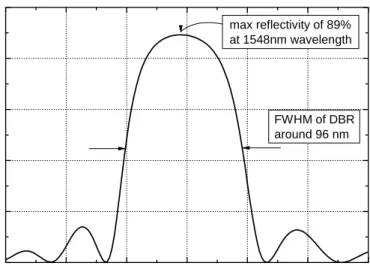
In the InP/Air DBR, the index difference is 2.167. Three pairs are enough to get 99.6% reflectivity with this structure. If the high reflectivity band of this structure is observed, it is seen that its FWHM is higher than 1000 nm. While InP/InAlGaAs DBR has index difference of only 0.293. This DBR needs 40 pairs to achieve 99.5% reflectivity. Also due to lower index contrast, FWHM is less than 100 nm.
With a small change in the design of the DBRs, the nature of these mirrors can be changed. If the width of one of the layers (with a refractive index of n1) increased from λc/4n1 to λc/2n1, the structure becomes transparent
around λc, while still reflecting other wavelengths. In this case, the multiplayer
stack functions as a notch filter. Such filters have been demonstrated at various wavelengths on both silicon and GaAs based devices [26-28]. Figure 2.13 shows the transmission spectra of notch filter, which consists of Si and SiO2
layers operating around 1550 nm.
1400 1450 1500 1550 1600 1650 1700 0 20 40 60 80 100 T ra n smission (%) Wavelength (nm)
Figure 2.13: Transmission spectrum of Si/SiO2 notch filter centered to 1550
Chapter 3
Fabrication and Characterization
This chapter presents the fabrication and characterization process that was completed in Advanced Research Laboratories at Bilkent University. Section 3.1 explains the basic fabrication steps, while section 3.2 presents the measurement setups.3.1 Basic Fabrication Steps
This section explains the details of fabrication steps completed in a Class-100 clean room environment. With the application of three or four of them, usually one fabrication step of the photodetectors are completed.
3.1.1 Sample Cleaving
The wafers that are used for the fabrication of photodetectors in this thesis are usually quite expensive and hard to grow. That’s why we prefer working with small samples cleaved from the wafer. Sample sizes are around 7×7 mm2
, and the mask is 6×6 mm2
. We use a diamond tipped scriber-pen to define a line at the back of the substrate. After defining the shape of the sample, the wafer can be easily cleaved. The thicknesses of the wafer are usually 350 µm for 3-inch wafers, and 600 µm for 4-inch wafers.
CHAPTER 3. FABRICATION AND CHARACTERIZATION 27
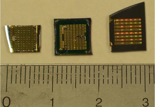
Figure 3.1: Photographs of some samples with fabricated photodetectors on them.
3.1.2 Sample Cleaning
The samples are cleaned at every step. The residues from the previous step must be cleaned. Three different solvents are used for the cleaning, namely trichloroethane, aceton, and isopropanol alcohol. Samples are dipped into them in order. The details of the cleaning are as follows:
• Samples are immersed into the boiling trichloroethane for 2 minutes. • Then the samples are kept in acetone at room temperature for 5 minutes.
Acetone dissolves organic molecules, and the photoresist.
• Next samples are kept in boiling isopropanol alcohol for 2 minutes. This alcohol cleans the residues from the previous step.
• Samples are rinsed in the de-ionized (DI) water flow and dried with nitrogen gun.
CHAPTER 3. FABRICATION AND CHARACTERIZATION 28
• Although the sample is dried with nitrogen flow, there remains a very thin layer of water at the surface. To evaporate this water, samples are baked at 120 oC on the hat plate for 2 minutes. This bake is called dehydration bake.
3.1.3 Photolithography
Before the fabrication, the mask is prepared which contains the features to be transformed onto the samples. The CAD program named Wavemaker is used for the preparation of the digital file. The features for each step are placed on 6×6 mm2
area. These features are the photodetectors, test diodes that does not contain interconnect metallization, ohmic test patterns, development marks that are used to check the quality of the photolithography and development, and the alignment marks that are used to align the mask with respect to the sample at each step. One mask usually contains 25 dies, where each die has the patterns for one lithography step. The size of the masks is 4×4 inch2
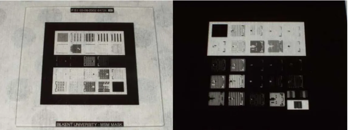
so that all the dies can be used with the mask aligner. Figure 3.2 shows photographs of our masks. Figure 3.3 has some plots from the digital mask file.
CHAPTER 3. FABRICATION AND CHARACTERIZATION 29
(a) (b)
(c) (d)
Figure 3.3: Plots from the mask file (a) a photodiode with 100 µm diameter active area, (b) development marks used in the p+ ohmic step, (c) p+ ohmic transmission lines and the development marks, and (d) alignment marks. Photolithography starts with covering the surface of the sample with a chemical, which contains polymer that is sensitive to ultraviolet radiation. This chemical is called photoresist. The AZ-5214E type photoresist produced by Clarient is used. To achieve a uniform thickness, the sample is spinned at 5000 rpm for 40 seconds. The thickness of the photoresist obtained after this spin is around 1.35 µm. The thickness can be changed by changing the spin rate [29]. This photoresist is sensitive to UV radiation in the 310 – 420 nm spectral range. The Karl-Suss MJB3 mask aligner is used for the alignment of the samples and exposure. The aligner has a mercury lamp that has a high power emission around 365 nm. Before the exposure, the sample is baked on a hot plate at
CHAPTER 3. FABRICATION AND CHARACTERIZATION 30
110oC for 55 seconds. This bake is called the soft-bake. At this point, the process can be varied to get both positive and negative resist.
Figure 3.4: Plot of the mask containing large area photodetectors. All the fabrication steps are shown aligned to each other. The mask contains around
115 photodetectors.
• Normal Photolithography: After the soft-bake, the sample is exposed with the mask with a total energy of 150 mJ/cm2. The
photoresist at the exposed area becomes soluble in the developer. • Image-reversal Photolithography: After the pre-bake, the sample
is exposed with the mask with a total energy of 50 mJ/cm2. Then the sample is baked at 110 oC for 2 minutes. The exposed photoresist becomes inert after this step. Then the whole sample area is exposed without a mask with a total energy of 150 mJ/cm2. Then the unexposed area in the first exposure becomes soluble in the developer. The explanation of this process is also shown in Figure 3.5.
CHAPTER 3. FABRICATION AND CHARACTERIZATION 31 substrate photoresist soluble inert soluble (1) Exposure using an
inverted mask (the exposed areas finally remain
(2) The resist now would
behave like an exposed positive resist
(3) The reversal bake
cross-links the exposed area, while the unexposed area remain
photo-active
(4) The Flood exposure
(without a mask) …
… (5) makes the resist, which was not exposed in
the first step, soluble in developer
(6) After development, the
areas exposed in the first step now remain
Figure 3.5: Image-reversal photolithography (after reference [30]).
3.1.4 Development
For the development of the exposed samples, AZ400K developer is used with a 1:4 (Developer:H2O) volume ratio. As the soluble regions of the resist are
etched by the developer, change in the color can be observed with naked eye. When this color change stops, the sample is rinsed under DI water. After drying the sample, the alignment and the development is checked. The resolution patterns must be sharp, and for a good photolithography about 1 µm resolution should be observable. The resolution of the image-reversal photolithography is less than the normal photolithography. The AZ400K developer contains metal ions and is based on potassium hydroxide. This developer affects the semiconductor layers containing Aluminum.
CHAPTER 3. FABRICATION AND CHARACTERIZATION 32
3.1.5 Etch
The etch process is used for transforming the defined patterns onto the underlying metal, semiconductor or dielectric layers, so that the desired layer is reached for the subsequent process. Etching is also used for cleaning and thinning photoresist, removing damaged material, polishing, and removing surface oxides. Etching is done in two different methods, either by using chemical reactants present in aqueous solution (wet etch) or with the help of ions and molecules present in a plasma (dry etch).
• Wet Etch: Chemical reactions that occur at the surface of the material with the reactants present in the solution. For the semiconductors, the etching is basically done by oxidation or reduction of the surface and then removal of the soluble reaction product. The etch rate may be limited by the transport of the reactants and the products. This type of etches are diffusion-controlled etches. This type of etch is usually anisotropic and agitation of the solution changes the etch rate and profile. The etch is called reaction-limited etch, if the reaction has a rate-limiting step. These type of etches can be isotropic, and the rate is insensitive to agitation [31]. We bake the resist at 120 oC for 1 min, to refrain the photoresist from the tension that occurs during the development. This bake enhances the adhesion to the substrate at the contours of the photoresist, which decreases the under-etch for deep etches. Figure 3.6 (a) shows a wet etch profile of GaAs where the under-etch is more than expected. Some of the etch recipes that are used in our lab are listed in Table 3.1.
CHAPTER 3. FABRICATION AND CHARACTERIZATION 33
Figure 3.6: SEM picture wet etch profiles.
(b)
(a)
Table 3.1: Etch rates of some recipes used in our processes.
Etchant Etched Layer Etch Rate
(nm/sec) H3PO4 : H2O2 : H2O (1:3:40) InGaAs, InAlAs 4.5, 5.0
HCl : H3PO4 (1:3) InP 12.5
H3PO4 : H2O2 : H2O (1:1:5) InAs 12.5
Citric acid : H2O2 (1:1) InSb ~ 0.4 - 0.5
HF : H2O2 : H2O (2:1:100) GaSb 30.0
NH3 : H2O2 : H2O (2:1:75) GaAs, Al0.2Ga0.8As 5.0, 8.1
• Dry Etch: Dry etching techniques use plasma-driven chemical reactions or energetic ion beams. Some of dry etching techniques are plasma etching, reactive ion etching (RIE), reactive ion-beam etching (RIBE), sputter etching, and ion milling. Plasma etch occurs either by the bombardment of the surface with highly energetic ions where the etching is made mechanically, or by the chemical reactions between the
CHAPTER 3. FABRICATION AND CHARACTERIZATION 34
gases and the surface. In the later, volatile products are generated which are pumped out of the reaction chamber. Changing the gas pressure and ion energy can control degree of isotropy. Usually higher gas pressure results isotropic etch. Ultra high vacuum (UHV) RIE machine is used for dry etching. With appropriate gases, dielectrics, semiconductors, resist, even metals can be etched with this system [32-34]. Currently CCl2F2, SF6, CHF3, O2, CF4, and H2 gases are available in our system.
Some of the recipes are listed in Table 3.2.
Table 3.2: Etch rates of some recipes used in RIE etch.
Plasma Condition Etch Results
RF Power : 51 W Pressure : 7 µBar O2 : 20 sccm
Self Bias : 350 V
Hardened Photoresist : 70 nm/min
RF Power : 51 W Pressure : 4 µBar CCl2F2 : 20 sccm Self Bias : 360 V GaAs : 100 nm/min Al0.3Ga0.7As : 30 nm/min Photoresist : 10 nm/min RF Power : 99 W Pressure : 10 µBar CCl2F2 : 20 sccm Self Bias : 490 V InP : 50 nm/min InGaAs : 55 nm/min Photoresist : 12 nm/min RF Power : 200 W Pressure : 15 µBar CH4 : 10 sccm H2 : 20 sccm O2 : 0 sccm Self Bias : 570 V InP : 36 nm/min (CH4 currently not available)
(Damages the photoresist) (Polymer deposition on the mask)
CHAPTER 3. FABRICATION AND CHARACTERIZATION 35 RF Power : 69 W Pressure : 20 µBar CHF3 : 60 sccm O2 : 5 sccm Self Bias : 350 V Si : 12.5 nm/min Si3N4 : 70 nm/min SiO2 : 1.1 nm/min Photoresist : 32 nm/min RF Power : 99 W Pressure : 8 µBar CCl2F2 : 20 sccm Self Bias : 490 V GaAs : 300 nm/min InAs : 60 nm/min Si3N4 : 40 nm/min SiO2 : 25 nm/min ITO : 20 nm/min Photoresist : 45 nm/min GaN : 31 nm/min Al0.38Ga0.62N : 13 nm/min
Hardened Photoresist : 22 nm/min RF Power : 150 W Pressure : 10 µBar CHF3 : 60 sccm O2 : 5 sccm Self Bias : 550 V SiO2 : 17 nm/min Photoresist : 42 nm/min
While most of the III-V semiconductors materials can be etched using a wet etch techniques, GaN and related materials cannot be etched easily in this way. We use only RIE with CCl2F2 gas to etch GaN and other wide band-gap
materials [35].
3.1.6 Metallization
Metals are deposited onto the sample for ohmic, Schottky, or interconnect metallization. Metals and dielectric coatings are deposited inside ultra high vacuum LE590 box coater, using thermal evaporation or radio frequency (RF) sputtering technique. In both methods, the pressure of the process chamber is lowered to 5×10⁻⁶
mBar. The deposition rate and the total thickness of the film are monitored during the process.


![Figure 4.1: Lattice parameter vs. energy gap of III-V compounds used with InP and GaAs based devices (after reference [61])](https://thumb-eu.123doks.com/thumbv2/9libnet/5779887.117294/68.892.238.742.265.792/figure-lattice-parameter-energy-compounds-gaas-devices-reference.webp)
![Figure 4.2: Charge drift velocity as a function of electric filed strength for various semiconductors (after reference [61])](https://thumb-eu.123doks.com/thumbv2/9libnet/5779887.117294/72.892.198.780.479.628/figure-charge-velocity-function-electric-strength-semiconductors-reference.webp)