Probing Voltage Drop Variations in Graphene with Photoelectron
Spectroscopy
Coskun Kocabas*
,†and Sefik Suzer*
,‡†Department of Physics and ‡Department of Chemistry, Bilkent University, Ankara 06800, Turkey
*
S Supporting InformationABSTRACT: We use X-ray photoelectron spectroscopy (XPS) for characterization of voltage drop variations of large area single-layer graphene on quartz substrates, by application of a voltage bias across two gold electrodes deposited on top. By monitoring the spatial variation of the kinetic energies of emitted C1s photoelectrons, we extract voltage variations in the graphene layer in a chemically specific format. The potential drop is uniform across the entire layer in the pristine sample but is not uniform in the oxidized one, due to cracks and/or morphological defects created during the oxidation process. This new way of data gathering reintroduces XPS as a major analytical tool for extracting electrical as well as chemical information about surface and/or nanostructured materials.
S
ynthesis of free-standing two-dimensional crystals1 pro-vides new opportunities to study fundamental science in reduced dimensions2 as well as to develop new technologies.3 Particularly, graphene is at the center because of its unique electronic and mechanical properties. Extremely high charge mobility4and optical transparency5together with the ability to be synthesized over large areas6 makes graphene a promising material as a high performance semiconductor and a trans-parent conducting film. These applications require electrical characterization of graphene at different length scales. Besides electrical characterization, chemical characterization is essential to monitor and control dopants/defects in graphene. Characterization tools that provide simultaneous electrical and chemical analysis are desirable to understand the ultimate limits as well as performance of graphene-based devices.Photon-based spectroscopic techniques, like UV−vis, Raman, and IR, have already been heavily utilized for chemical characterization of graphene-based materials. In particular, Raman spectroscopy has been very successful in identifying number of layers, crystal structure, defects, and doping levels.7,8 Moreover, since Raman scattering in graphene involves a double-resonance process, energy, full-width at half-maxima, and intensity of G-band and 2D-band provide indirect information about the local doping levels.9 Correlation of Raman parameters provides information about some of the electrical and chemical properties of graphene.10 Infrared
spectroscopy has also been used to probe electrical and optical properties of graphene.11−13 Recently, Basov et al.14,15 combined infrared spectroscopy and scanning probe micros-copy to reveal the effects of substrates on the local electrical properties of graphene. Scanning probe microscopy techniques, such as Kelvin probe microscopy,16 scanning photocurrent microscopy,17and electrostatic force microscopy18 have been implemented to understand local electrical and chemical properties of graphene.
Electron-based surface characterization methods are well-established analytical tools to analyze chemical and physical parameters of materials. Many of these methods have also been utilized to probe properties of graphene. Auger electron spectroscopy19of graphene provides useful information about the number of layers and defect density. Wang et al. used energy loss spectroscopy to monitor bonding of lithium in intercalated graphite.20 Chemical analysis of graphene and graphene oxidefilms, after heat and chemical treatments, have been performed by X-ray photoelectron spectroscopy (XPS).21 For example, the binding energy of C1s can provide insight about the interaction between graphene and the underlying
Received: February 6, 2013 Accepted: March 16, 2013 Published: March 17, 2013
Article
substrate.22XPS has also been utilized for probing numerous chemical as well as electrical properties.23−35 In-situ electrical measurements during imaging with transmission electron microscopy provides correlation of atomic structure and electrical conductivity of graphene.36−38
One important aspect of the electron-based techniques is that they are also very susceptible to local electrical potentials created, intentionally or not, in the materials analyzed. In most cases, such potentials are due to charging, which has been an obstacle, and should be eliminated.39However, introduction of electrical potentials as a bias can also be an experimental asset for harvesting additional electrical information in a chemically specific format. For example, we have recently shown that XPS data of devices under working conditions can be recorded. This, so named, operando XPS, traces chemical and location-specific surface potential variations across a working CdS based photoresitor.40 By mapping Cd3d binding energy variations, we were able to obtain photoconductivity, electric field distribution, and identify some morphological defects. In a Si-diode, measurements of the position of the Si2p peak enabled us to separate and identify the p- and n-doped regions and/or domains.41In this letter, we extend our methodology to XPS characterization of voltage drop variations of large area single-layer graphene, in a chemically specific fashion.
■
EXPERIMENTAL SECTIONWe used a Thermo Fisher K-alpha electron spectrometer with a monochromatic Al Kα X-ray source (hν = 1486.6 eV). We
slightly modified the spectrometer to apply an external voltage bias across the samples. The samples consist of large area (1 cm × 1 cm) graphene that was transfer-printed on a quartz substrate. To apply a bias voltage to the graphene layer, we fabricated two gold electrodes with a thickness of 50 nm, using standard UV-photolithography and metallization process. The gap between the electrodes is around 1−4 mm. The graphene samples, prior to contact transfer to the quartz substrate, were synthesized on copper foils with chemical vapor deposition.42 The copper foils were placed in a quartz chamber and heated to 1000°C under a flow of hydrogen and argon. We annealed the foils at 1000 °C for 20 min before the growth. A mixture of methane and hydrogen (7 sccm CH4and 7 sccm H2) was used
as the reaction gas. The chamber pressure was kept at 300 mTorr during the growth. Stopping the flow of methane terminated the growth, and then, the chamber was cooled back to room temperature. After the growth, the graphene layers were transfer-printed to quartz substrates.43 This was accomplished by spin coating the copper foils with a thin layer of photoresist (PR, AZ5214). A flat elastomeric stamp (polydimethylsiloxane, PDMS) was placed on the PR layer, and the copper foil was etched away by 1.0 M ferric chloride solution. After the etching process, the PR layer with graphene remains on the PDMS stamp. The stamp was then applied on quartz substrates and heated to 80°C to release the PR. After removing the stamp, the PR layer was removed by dissolving in acetone. We used Raman spectroscopy to evaluate the quality and uniformity of the graphene samples on quartz substrates.
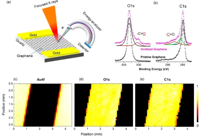
Figure 1.(a) Schematic representation of the experimental setup used for X-ray photoelectron spectroscopy on graphene. A microfocused X-ray beam with a 30μm spot size is scanned along the graphene layer between two gold electrodes. The distance between the electrodes is 1.5 mm. The beam is scanned at 100μm steps. (b) XPS spectra of slightly oxidized and pristine graphene on quartz substrates. (c−e) Areal maps for each element; Au4f (electrode), C1s (graphene), and O1s (mainly of the quartz substrate) peaks.
The line width of 2D peak and the intensity ratio of 2D to G bands are 32 cm−1 and 2.4, respectively. To oxidize the graphene layers, we exposed the samples to mild oxygen plasma (5 W RF power with 20 sccm flow of O2) in a reactive ion
etching system. After 2 s of oxidation, the resistance of the device increased from 300Ω to 1.2 kΩ. We also measured the Raman spectra of the oxidized graphene. After the oxidation, the intensity of the 2D band decreased and that of the D band increased. The intensity ratios of 2D/G and D/G were around 1.0 and 1.2, respectively. Raman spectra of the pristine and oxidized graphene samples are given in the Supporting Information.44
■
RESULTS AND DISCUSSIONSConventional XPS analysis together with elemental maps provide detailed bonding information for both pristine graphene as well as its slightly oxidized form(s), as was done for our samples shown in Figure 1, where both the oxidized
C1s and the corresponding O1s peaks appear as well-separated peaks. We go one step further and apply a voltage bias across the graphene layer lying between the two gold electrodes, during the acquisition of XPS data. By monitoring the spatial variation of the measured kinetic energies of the emitted C1s and O1s photoelectrons, we are able to map the voltage variations in the graphene layer in a chemically specific fashion. In addition to the value obtained from Einstein’s equation (K.E. = hν − B.E. + Φ), the measured kinetic energy of the emitted photoelectrons is now affected by the local electrostatic interactions, charge density, and external voltage bias. The surface potentials can be obtained from the shifts in the measured binding/kinetic energy at a precision of 0.05 eV or better.
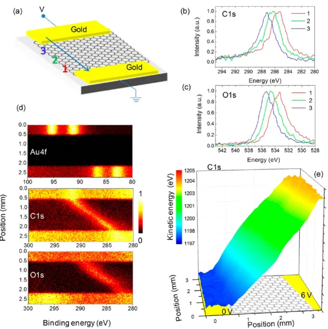
Figure 2a shows the schematic representation of the experiential setup. A +6 V bias was applied between the gold electrodes, and Au4f, C1s, and O1s peaks were recorded in the snapshot mode, with an X-ray spot size of 30 and 100μm steps
Figure 2.(a) Schematic representation of a graphene device under a voltage bias used for probing voltage drop on graphene using XPS. We ground one of the electrodes and apply +6 V external voltage bias to the other electrode. (b and c) C1s and O1s region of the XPS spectrum of graphene on SiO2substrate recorded at three different points between the electrodes. (d) False color contour plot of XPS line scan spectra for Au4f7/2, C1s, and
O1s regions. (e) 3D areal map for C1s kinetic energy of graphene in the channel between the electrodes.
over an area of 4 × 4 mm, including the electrodes. The resulting data set is immense and can be converted to areal maps and line-scans for each element; Au4f (electrode), C1s (graphene), and O1s (mainly of the quartz substrate) peaks are shown in Figure 2b at three chosen points. As can be gathered from thefigure, their peak positions vary linearly with respect to the voltage drop across the device. The surprising fact is that the O1s of the substrate faithfully follows the C1s of the graphene. In Figure 2d, Au4f, C1s, and O1s spectra along the designated line-scan is displayed, all of which exhibit a smooth resistive voltage drop across the electrodes, as is also confirmed in Figure 2e by the false-color areal image of the C1s peak positions.
The information content of the displayed data is very rich and can be used to extract other properties. For example, the measured 6.00 ± 0.05 eV binding energy difference between the Au4f peaks on the two electrodes matches exactly the applied +6.00 V bias and reveals to us that no significant contact resistances exist within our experimental setup. The C1s peak also exhibits a 6.00 ± 0.08 eV binding energy difference. Moreover, the measured binding energy difference of 200.75 ± 0.08 eV between the Au4f7/2 (84.00) and C1s
(284.75) peaks at both electrodes signals the absence of any measurable contact potentials between the gold electrodes and our graphene sample over as large a contact distance as 3−4 mm.15 As mentioned above, the O1s peak of the quartz substrate follows the voltage variations without the need of flood-gun neutralization. The presence of graphene provides equipotential surfaces across the device which prevents charging of the dielectric substrate. However, as shown in Figure 3a and b, the binding energy difference between the C1s and the O1s exhibits afluctuation of 0.05 eV about the mean value of 247.9 eV, which matches exactly the tabulated binding energy difference.39 The areal map of the binding energy
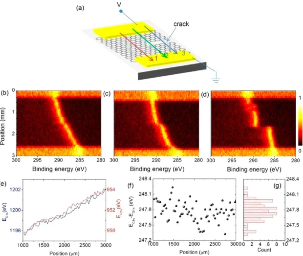
variation and its histogram are given in Figure 3d and e, respectively. The gap between the graphene and substrate, local multilayerflakes, and/or the local conductivity created by the focused X-rays could cause the variations/fluctuations of the binding energy difference between the C1s and the O1s. Even though the exact mechanism is unclear at this point, as will be shown below, such measurements can reveal information about structural and/or morphological defects of the graphene layer. In Figure 4, we display similar spectral features of the same graphene sample after oxidation, where the voltage drop variations are no longer smooth throughout the sample area, due mainly to the cracks and/or morphological defects formed during the latter process. Figure 4a shows a schematic representation of a crack on the graphene layer. By monitoring the voltage, we were able to locate such cracks on the graphene layer and have measured the binding energy variation of the C1s on the defective graphene layer under a voltage bias of 6 V. Figure 4b and c shows the peak positions of the C1s for three line scans at different positions relative to the crack. Initially the binding energy varies linearly with the position; however, as we move along the line scan on the crack, the linearity becomes perturbed and binding energy becomes constant indicating no local current is passing through the graphene. Furthermore, after the oxidation, the overall variation between the binding energies of C1s and O1s increased significantly. Figure 4e shows the measured C1s of graphene and O1s of the substrate (SiO2) kinetic energy positions along the XPS line scan. The
difference between the measured kinetic energy positions of C1s and O1s and its histogram are given in Figure 4f and g, respectively. The standard deviation of the binding energy difference is significantly increased to 0.2 eV due to the presence of cracks/defects. Note that, characterization using electrical means only would not have revealed this information about the electrical properties. Electrical measurement could
Figure 3.(a) Variation of measured kinetic energy of C1s and O1s as a function of the position between the gold electrodes. (b) Difference between the measured kinetic energy of C1s and O1s. (c) Histogram of the distribution of the kinetic energy difference for the line scan. (d) False color map of the areal scan of kinetic energy difference of C1s and O1s in the channel area between the electrodes. (e) Histogram of kinetic energy difference for the areal map. The standard deviation of the histogram is 0.05 eV.
only provide total resistance of the device. As mentioned above, after the oxidation process with mild oxygen plasma, the total resistance of the devices increased from 300Ω to 1.2 kΩ.
■
CONCLUSIONSIn summary, we use X-ray photoelectron spectroscopy for characterization of voltage drop variations of large area single-layer graphene on quartz substrates, by imposing a voltage bias across the two gold electrodes deposited on top. By monitoring the spatial variation of the kinetic energies of emitted photoelectrons, we extract voltage variations in graphene layers in a chemically specific format, which is found to be uniform across the entire layer in the pristine sample but is not uniform in the oxidized one, due to cracks and/or morphological defects created during the oxidation process. This method traces chemical and location specific surface potential variations across a working graphene device in a chemically addressed format. Furthermore, owing to high conductivity of graphene and being electron transparent, the graphene overlayer prevents charging of dielectric substrates by yielding equipotential surfaces.
■
ASSOCIATED CONTENT*
S Supporting InformationRaman spectra of the pristine and oxidized graphene samples and histograms of areal maps. This material is available free of charge via the Internet at http://pubs.acs.org.
■
AUTHOR INFORMATIONCorresponding Author
*E-mail: [email protected] (C.K.), suzer@fen. bilkent.edu.tr (S.S.).
Notes
The authors declare no competingfinancial interest.
■
REFERENCES(1) Novoselov, K. S.; Jiang, D.; Schedin, F.; Booth, T. J.; Khotkevich, V. V.; Morozov, S. V.; Geim, A. K. Proc Natl Acad Sci USA 2005, 102 (30), 10451−3.
(2) Novoselov, K. S.; Geim, A. K.; Morozov, S. V.; Jiang, D.; Katsnelson, M. I.; Grigorieva, I. V.; Dubonos, S. V.; Firsov, A. A. Nature 2005, 438 (7065), 197−200.
(3) Lin, Y. M.; Valdes-Garcia, A.; Han, S. J.; Farmer, D. B.; Meric, I.; Sun, Y. N.; Wu, Y. Q.; Dimitrakopoulos, C.; Grill, A.; Avouris, P.; Jenkins, K. A. Science 2011, 332 (6035), 1294−1297.
(4) Bolotin, K. I.; Sikes, K. J.; Jiang, Z.; Klima, M.; Fudenberg, G.; Hone, J.; Kim, P.; Stormer, H. L. Solid State Commun. 2008, 146 (9− 10), 351−355.
Figure 4.(a) Schematic representation of a graphene device containing a defected region (after oxidation) under a +6 V bias. (b−d) Line scans of C1s region of the XPS spectra near a defected region on the graphene layer. (e) Measured C1s of graphene and O1s of the substrate (SiO2) kinetic
energy positions along the XPS line scan. (f) Difference between the measured kinetic energy of C1s and O1s. (g) Histogram of the distribution of the kinetic energy difference for the line scan. The standard deviation of the histogram is 0.2 eV.
(5) Nair, R. R.; Blake, P.; Grigorenko, A. N.; Novoselov, K. S.; Booth, T. J.; Stauber, T.; Peres, N. M.; Geim, A. K. Science 2008, 320 (5881), 1308.
(6) Bae, S.; Kim, H.; Lee, Y.; Xu, X.; Park, J. S.; Zheng, Y.; Balakrishnan, J.; Lei, T.; Kim, H. R.; Song, Y. I.; Kim, Y. J.; Kim, K. S.; Ozyilmaz, B.; Ahn, J. H.; Hong, B. H.; Iijima, S.Nat Nanotechnol 2010, 5 (8), 574−8.
(7) Ferrari, A. C. Solid State Commun. 2007, 143 (1−2), 47−57. (8) Dresselhaus, M. S.; Jorio, A.; Hofmann, M.; Dresselhaus, G.; Saito, R. Nano Lett. 2010, 10 (3), 751−758.
(9) Das, A.; Pisana, S.; Chakraborty, B.; Piscanec, S.; Saha, S. K.; Waghmare, U. V.; Novoselov, K. S.; Krishnamurthy, H. R.; Geim, A. K.; Ferrari, A. C.; Sood, A. K.Nat Nanotechnol 2008, 3 (4), 210−5.
(10) Kalbac, M.; Reina-Cecco, A.; Farhat, H.; Kong, J.; Kavan, L.; Dresselhaus, M. S. Acs Nano 2010, 4 (10), 6055−6063.
(11) Yan, H. G.; Xia, F. N.; Zhu, W. J.; Freitag, M.; Dimitrakopoulos, C.; Bol, A. A.; Tulevski, G.; Avouris, P. Acs Nano 2011, 5 (12), 9854− 9860.
(12) Jiang, Z.; Henriksen, E. A.; Tung, L. C.; Wang, Y. J.; Schwartz, M. E.; Han, M. Y.; Kim, P.; Stormer, H. L. Phys. Rev. Lett. 2007, 98 (19), No. 197403.
(13) Acik, M.; Lee, G.; Mattevi, C.; Pirkle, A.; Wallace, R. M.; Chhowalla, M.; Cho, K.; Chabal, Y. J. Phys. Chem. C 2011, 115 (40), 19761−19781.
(14) Fei, Z.; Rodin, A. S.; Andreev, G. O.; Bao, W.; McLeod, A. S.; Wagner, M.; Zhang, L. M.; Zhao, Z.; Thiemens, M.; Dominguez, G.; Fogler, M. M.; Neto, A. H. C.; Lau, C. N.; Keilmann, F.; Basov, D. N. Nature 2012, 487 (7405), 82−85.
(15) Fei, Z.; Andreev, G. O.; Bao, W. Z.; Zhang, L. F. M.; McLeod, A. S.; Wang, C.; Stewart, M. K.; Zhao, Z.; Dominguez, G.; Thiemens, M.; Fogler, M. M.; Tauber, M. J.; Castro-Neto, A. H.; Lau, C. N.; Keilmann, F.; Basov, D. N. Nano Lett. 2011, 11 (11), 4701−4705.
(16) Yan, L.; Punckt, C.; Aksay, I. A.; Mertin, W.; Bacher, G. Nano Lett. 2011, 11 (9), 3543−9.
(17) Mueller, T.; Xia, F.; Freitag, M.; Tsang, J.; Avouris, P. Phys. Rev. B 2009, 79 (24), No. 245430.
(18) Burnett, T.; Yakimova, R.; Kazakova, O. Nano Lett. 2011, 11 (6), 2324−2328.
(19) Xu, M.; Fujita, D.; Gao, J.; Hanagata, N.ACS Nano 2010, 4 (5), 2937−45.
(20) Wang, F.; Graetz, J.; Moreno, M. S.; Ma, C.; Wu, L.; Volkov, V.; Zhu, Y.ACS Nano 2011, 5 (2), 1190−7.
(21) Yang, D.; Velamakanni, A.; Bozoklu, G.; Park, S.; Stoller, M.; Piner, R. D.; Stankovich, S.; Jung, I.; Field, D. A.; Ventrice, C. A.; Ruoff, R. S. Carbon 2009, 47 (1), 145−152.
(22) Brako, R.; Sokcevic, D.; Lazic, P.; Atodiresei, N. New J. Phys. 2010, 12.
(23) Busse, C.; Lazic, P.; Djemour, R.; Coraux, J.; Gerber, T.; Atodiresei, N.; Caciuc, V.; Brako, R.; N’Diaye, A. T.; Blugel, S.; Zegenhagen, J.; Michely, T. Phys. Rev. Lett. 2011, 107 (3), No. 36101. (24) Chiu, P. L.; Mastrogiovanni, D. D. T.; Wei, D. G.; Louis, C.; Jeong, M.; Yu, G.; Saad, P.; Flach, C. R.; Mendelsohn, R.; Garfunkel, E.; He, H. X. J. Am. Chem. Soc. 2012, 134 (13), 5850−5856.
(25) Eckmann, A.; Felten, A.; Mishchenko, A.; Britnell, L.; Krupke, R.; Novoselov, K. S.; Casiraghi, C. Nano Lett. 2012, 12 (8), 3925− 3930.
(26) Filleter, T.; Emtsev, K. V.; Seyller, T.; Bennewitz, R. Appl. Phys. Lett. 2008, 93 (13), No. 133117.
(27) Hammock, M. L.; Sokolov, A. N.; Stoltenberg, R. M.; Naab, B. D.; Bao, Z. A. ACS Nano 2012, 6 (4), 3100−3108.
(28) Kim, M.; Safron, N. S.; Huang, C. H.; Arnold, M. S.; Gopalan, P. Nano Lett. 2012, 12 (1), 182−187.
(29) Larciprete, R.; Lacovig, P.; Gardonio, S.; Baraldi, A.; Lizzit, S. J. Phys. Chem. C 2012, 116 (18), 9900−9908.
(30) Perera, S. D.; Mariano, R. G.; Vu, K.; Nour, N.; Seitz, O.; Chabal, Y.; Balkus, K. J. ACS Catal. 2012, 2 (6), 949−956.
(31) Prezioso, S.; Perrozzi, M.; Donarelli, M.; Bisti, F.; Santucci, S.; Palladino, L.; Nardone, M.; Treossi, E.; Palermo, V.; Ottaviano, L. Langmuir 2012, 28 (12), 5489−5495.
(32) Rana, K.; Kucukayan-Dogu, G.; Sen, H. S.; Boothroyd, C.; Gulseren, O.; Bengu, E.J. Phys. Chem. C 2012, 116 (20), 11364− 11369.
(33) Usachov, D.; Vilkov, O.; Gruneis, A.; Haberer, D.; Fedorov, A.; Adamchuk, V. K.; Preobrajenski, A. B.; Dudin, P.; Barinov, A.; Oehzelt, M.; Laubschat, C.; Vyalikh, D. V. Nano Lett. 2011, 11 (12), 5401− 5407.
(34) Wang, S. N.; Wang, R.; Liu, X. F.; Wang, X. W.; Zhang, D. D.; Guo, Y. J.; Qiu, X. H. J. Phys. Chem. C 2012, 116 (19), 10702−10707. (35) Wei, D. C.; Liu, Y. Q.; Wang, Y.; Zhang, H. L.; Huang, L. P.; Yu, G. Nano Lett. 2009, 9 (5), 1752−1758.
(36) Xu, Z.; Bando, Y.; Liu, L.; Wang, W. L.; Bai, X. D.; Golberg, D. ACS Nano 2011, 5 (6), 4401−4406.
(37) Ho, P.-H.; Yeh, Y.-C.; Wang, D.-Y.; Li, S.-S.; Chen, H.-A.; Chung, Y.-H.; Lin, C.-C.; Wang, W.-H.; Chen, C.-W. ACS Nano 2012, 6 (7), 6215−6221.
(38) Tsen, A. W.; Brown, L.; Levendorf, M. P.; Ghahari, F.; Huang, P. Y.; Havener, R. W.; Ruiz-Vargas, C. S.; Muller, D. A.; Kim, P.; Park, J. Science 2012, 336 (6085), 1143−1146.
(39) Briggs, D. S., M. P. Practical Surface Analysis: Auger and X-ray photoelectron spectroscopy, 2nd ed.; John Wiley & Sons: Chichester, 1996.
(40) Sezen, H.; Suzer, S. Anal. Chem. 2012, 84, 2990−2994. (41) Suzer, S. Anal. Meth.−UK 2012, 4 (11), 3527−3530. (42) Li, X. S.; Cai, W. W.; An, J. H.; Kim, S.; Nah, J.; Yang, D. X.; Piner, R.; Velamakanni, A.; Jung, I.; Tutuc, E.; Banerjee, S. K.; Colombo, L.; Ruoff, R. S.Science 2009, 324 (5932), 1312−1314.
(43) Salihoglu, O.; Balci, S.; Kocabas, C.Appl. Phys. Lett. 2012, 100 (21), No. 213110.
(44) See the Supporting Information.