©BEYKENT UNIVERSITY
A REDUNDANT ADDER STRUCTURE SUITABLE FOR THE NEW GENERATION RECONFIGURABLE FPGA
ARCHITECTURES
Uğur ÇİNİ1, Avni MORGÜL2
1Boğaziçi University Department of Electrical and Electronics
2
Engineering, [email protected], Beykent University, Department of Electronics and Communication Engineering,
ABSTRACT
Arithmetic operations are generally slowest operations in digital design which is the bottleneck in most of the systems. Optimizing adder circuits provides faster performance in arithmetic circuits. Field Programmable Gate Arrays (FPGA) are very popular to implement logic circuits. 6-input Look-Up Table (LUT) devices are on the market which dramatically increases the performance. In this paper, alternative addition structures, based on redundant carry-free arithmetic and suitable for 6 input LUT devices, are presented. A new double carry-save addition architecture is proposed, which reduces the critical path of the addition process for 6-input LUT devices. Key Words - FPGA, Redundant Arithmetic, Multilevel Logic
ÖZET
Genelde sayısal sistemlerde en yavaş işleyen kısımlar aritmetik işlem üniteleri olup sisitemin hızını belirleyen bu ünitelerdir. Aritmetik işlemlerin temeli olan toplama devrelerinin optimizasyonu ile bu üniteler hızlandırılabilir. Kullanıcı tarafından programlanabilen kapı dizileri (FPGA) lojik devreleri gerçeklemek için kullanılan en yaygın elemanlardır. Artık 6-Girişli dönüştürme tablosu (LUT) olan FPGA elemanları piyasaya çıkmıştır ve bu elemanları kullanarak aritmetik üniteleri hızlandırmak mümkündür. Bu makalede 6-Girişli dönüştürme tablosu (LUT) olan FPGA elemanları için uyarlanmış elde işlemi yapmayan, artık sayı sistemli aritmetik (redundant carry-free arithmetic) kullanan bir algoritma ve bunu gerçekleştirecek devreler sunulmaktadır. Anahtar kelimeler - FPGA, Artık sayı sistemleri, Çok seviyeli lojik
1. INTRODUCTION
Reconfigurable systems are having more and more application areas as the technology of the devices evolves. Nowadays, many of the high performance systems are being implemented efficiently using Field Programmable Gate Array (FPGA) devices. When the FPGA systems were first introduced, the main purpose was to emulate a digital system in a reconfigurable structure for verifying the functional correctness of the system. In today's technology, FPGAs are not only used for emulation and testing, many of the complex digital systems are implemented using FPGAs, especially in the areas of digital signal processing and hardware based cryptology.
FPGAs are composed of look-up tables (LUTs) which are the memory blocks of truth tables [1]. The LUT units in FPGAs generally contain efficient look-up table structures together with fast arithmetic unit inputs and outputs and registers for synchronous digital design. Complex digital systems can be synthesized into LUT units together with the routing information between each LUT unit. Generic FPGAs are based on 4-input LUTs, where a 4-input LUT can provide 4-variable truth table with 24 combinations. New generation FPGA technologies offer
6-input LUT devices where complex logic functions with 6 variables can be implemented efficiently and faster [2, 3].
Arithmetic operations are generally the slowest operations in digital systems. For fast digital systems, arithmetic units, especially adders and multipliers should be optimized. Simple binary addition requires carry propagation. The circuits gets slower whenever bit size of the operands increases. On the other side, redundant number systems provide carry-free arithmetic, where the bits of the operands. Two well-known, simple redundant systems carry propagation is limited and is not dependent on the number of are "binary signed digit (borrow-save)" and "carry-save" arithmetic.
Redundant number systems are the number systems where a number can be represented in alternative ways. The redundancy means extra information to represent a number, for breaking the carry propagation chains of the addition process. It is very useful when building arithmetic circuits, such as adders, adder trees, multipliers, etc.
In this work, carry-save adder operation is analyzed and compared to conventional addition operation. Then, the implementation of this method in new generation 6-input LUT based reconfigurable devices are shown. Carry-save structures can be efficient especially for the operations that require recursive addition operations, such as matrix multiplication and convolution operations used in finite impulse response (FIR) digital filters, and similar signal processing structures [4]. Moreover, a new double carry-save addition architecture is proposed, which reduces the critical path of the addition process for 6-input LUT devices. Double carry-save structure for redundant arithmetic is defined and the advantages for the 6-input LUT based FPGAs are addressed in the paper.
2. REDUNDANT NUMBER ADDERS
In simple arithmetic systems, addition of two numbers requires carry propagation. After addition of each digit, the carry-out signal propagates until the most significant bit is reached. This process increases the total addition time, which is not acceptable in many of the high performance systems. Redundant arithmetic structures are used for the removal of these carry chains [5, 6] and reduces the computation time drastically. Redundant number representation techniques for carry-free arithmetic is classified as signed-digit systems and carry-save structures.
A redundant number is a representation form of binary umbers by using more than necessary 2n bits, where n is the
number of digits to represent the maximum number in binary form. The basic idea of the redundant structures is storing
numbers in the form of X = A + B (carry save structures) or X =
A - B (signed digit structures). In this representation the carry
information is stored in the redundant bit and it does not propagate. A standard carry-propagate adder (or subtractor) is only required whenever a conventional result is needed [7, 8]. Two binary numbers can be added by using full-adder circuits. The single bit full adder cell and multi-bit binary addition scheme is shown in Fig. 1.a and 1.b. Here, single bit addition process can be defined as
x + y + Ci = 2cout + s (1) where x, y, cu and cout are all binary numbers, i.e. they all are
defined in the set of {0, 1} and '+' is the arithmetic addition. A full adder circuit may be interpreted as the simplest member of multi-operand (m,n) counter circuits. The (m, k) counters, where m is the number of input operands and k is the number of output digits, can be defined as [9]:
k - 1 m - 1
I ^ 2 = I x, ( 2 )
j=0 i=0
In (3, 2) counter, three binary numbers are added up and the result is given by two numbers. The operation of a (3, 2) counter can be described as
x + y + z = 2c +s which is equivalent to Eq. 1.
3. CARRY-SAVE ARITHMETIC AND ITS IMPLEMENTATION
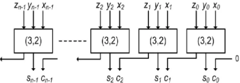
Fig. 2.a shows a basic carry-save adder structure where Xand Y are two normal binary numbers and the third number Z is defined as Z = S + C. The basic cell in the circuit is the (3, 2) counter which is equivalent to simple full adder. As the name implies, the carry component is saved inside the summation result. Here,
X = x3x2x1x0, Y= y y y y and Z = z3z2z1z0 and the result is
represented as Z = s ^ s s + c3c2c1c0. In carry-save format. Each
digit in Z can be represented by two bits as zt = {s*, c} and each digit value of Zi is equal to:
Zi = Si + Ci (3)
In carry save format, the addition is not finalized and the result is represented as the addition of two operands [4]. Whenever the normal binary mode result is required, at final stage of the adder, the two components of Z are added up.
Figure 1. a) Single bit full adder; b) Multi-bit full adder
Sn-1,x Cn-1,x
(3.2)
£
(3,2)
S2,y C2y Si y Cl y Sgy Co.y
Sî.i C2.X Six C1lX So,x Co.x
(3,2) (3,2) (3,2) (3,2) (3,2)
i t
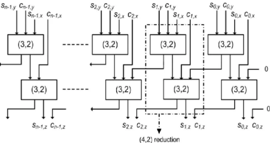
(3,2) r ~ * — i r ^ ^ - i - F ' r Sn-U Cn-),z S2,z C2,z ^ SU Cji Z SoiZ Co,z (4,2) r e d u c t i o nFig. 2. b) The final stage of the classical carry save adder structure
This final addition requires a standard carry propagate adder. Fig. 2.a shows the input stage of the counter and Fig.2.b represents the final addition stage of two numbers where each of the inputs and the output are in carry-save format. Here, addition of two redundant numbers are accomplished in two stage of (3, 2) counters, the reduction is also named as (4, 2) reduction, or (4, 2) compressor.
4. PROPOSED DOUBLED CARRY-SAVE ADDER ARCHITECTURE
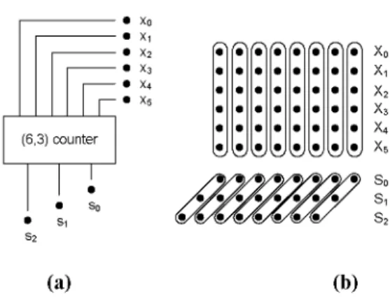
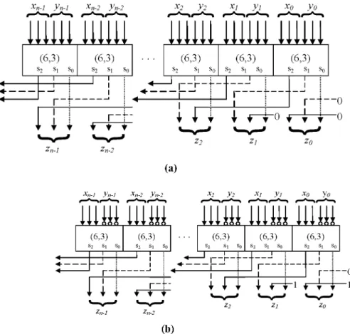
In this work, (6, 3) counters are used to exploit the advantages of 6-input LUT based FPGAs. Here, six binary inputs are added up with three-bit outputs. Single bit and multi-bit addition scheme with (6, 3) counters can be seen in Fig. 3. The 6 operands are reduced to 3 as the name of the counter circuit i.e. (6, 3) implies. The (6, 3) counters can be synthesized into a single stage whenever 6-input LUT devices are used for the implementation.
(6,3) counter T So Xo X, X2 X3 X4 X5 So S, S2 (a) (b)
Figure 3. (6, 3) counter: (a) single bit structure (b) addition of multiple operands using counters
In conventional carry-save structures, the carry save result is held by two operands, i.e. Z= S + C. In this work, six normal binary operands will be added up by using a single stage 6-input LUT device. So, we define a double carry-save operation. Each output of Fig.2 and the redundant sum Z is defined as:
Za = s0
Zb= Si<<J
Z = S2<<2 Z = Za + Zb + Z
where "<< k" operator defines left shift by k.
(3 a) (3.b) (3.c) (3.d)
One bit of the redundant sum consists of composition of three-bit set zi = [zai, zbi, zci}. As a result, each bit of Zi can have values between 0 (za; + zb, + zc, = 0) to 3 (za; + zb, + zc, = 3). In this structure, each summation digit is represented by 3 bits (as shown in Fig. 3) where conventional carry-save system (as shown in Fig. 2.a and Fig.2.b) the result is represented by 2 bits. Since each result is represented by 3-bit set, two results can be added up using one stage 6-input LUT device and computed in a single step.
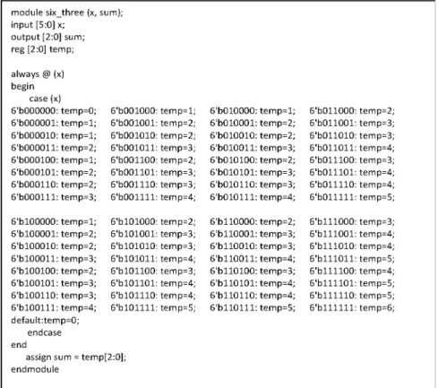
module six_three (x, sum); input [5:0] x; output [2:0] sum; reg [2:0] temp; always @ (x) begin case (x)
6'b000000 temp= 0; 6'b001000 temp= 1; 6'b010000 temp= 1; 6'b011000 temp= 2; 6'b000001 temp= 1; 6'b001001 temp= 2; 6'b010001 temp= 2; 6'b011001 temp= 3; 6'b000010 temp= 1; 6'b001010 temp= 2; 6'b010010 temp= 2; 6'b011010 temp= 3; 6'b000011 temp= 2; 6'b001011 temp= 3; 6'b010011 temp= 3; 6'b011011 temp= 4; 6'b000100 temp= 1; 6'b001100 temp= 2; 6'b010100 temp= 2; 6'b011100 temp= 3; 6'b000101 temp= 2; 6'b001101 temp= 3; 6'b010101 temp= 3; 6'b011101 temp= 4; 6'b000110 temp= 2; 6'b001110 temp= 3; 6'b010110 temp= 3; 6'b011110 temp= 4; 6'b000111 temp= 3; 6'b001111 temp= 4; 6'b010111 temp= 4; 6'b011111 temp= 5; 6'b100000 temp= 1; 6'b101000 temp= 2; 6'b110000 temp= 2; 6'b111000 temp= 3; 6'b100001 temp= 2; 6'b101001 temp= 3; 6'b110001 temp= 3; 6'b111001 temp= 4; 6'b100010 temp= 2; 6'b101010 temp= 3; 6'b110010 temp= 3; 6'b111010 temp= 4; 6'b100011 temp= 3; 6'b101011 temp= 4; 6'b110011 temp= 4; 6'b111011 temp= 5; 6'b100100 temp= 2; 6'b101100 temp= 3; 6'b110100 temp= 3; 6'b111100 temp= 4; 6'b100101 temp= 3; 6'b101101 temp= 4; 6'b110101 temp= 4; 6'b111101 temp= 5; 6'b100110 temp= 3; 6'b101110 temp= 4; 6'b110110 temp= 4; 6'b111110 temp= 5; 6'b100111 temp= 4; 6'b101111 temp= =5; 6'b110111 temp= 5; 6'b111111 temp= 6; default:temp=0;
endcase end
assign sum = temp[2:0]; endmodule
Figure 4. Verilog definition of (6, 3) counter
A single digit (6, 3) counter can be synthesized using a 6-input LUT using verilog HDL (Hardware Description Language) statements seen in Fig. 4. Here, each definition of the input is defined using 'case' statements to make compiler directly synthesize expected LUT configuration.
In this redundant representation, each digit of the redundant variable is composed of three bits. Addition of two redundant variables with result Z = X + Y can also be implemented using one stage of 6-input LUT structure as seen in Fig. 5.a where X, Y, and Z are all in double carry-save format. Here, for each digit,
three LUT elements are required to generate the output, since each digit is composed of three bits. Each digit of the three variables, X, Y and Z consists of three bit sets, i.e. Z = zn-1 zn-2 ...
Z1 zo; X=xn-1 Xn-2 . Xi xo; Y = yn-1 yn-2 ••• yiyo and each digit is in
the set of xu yt and zte {0, 1, 2, 3}.
xn-1 yn-1 xn-2 yn-2 x2 y2 xi y i xo yo
(6,3) (6,3)
s2 s1 s0 s2 s1 s0
im min min iiuu
r r I I • • Zn-l (6,3) s2 s1 s0 1 .hZ-LZT' _L
r
+ t t Zn-2i r n
(6,3) s2 s1 s0 —i—r
(6,3) s2 s1 s0 I _L Z2 t t - o r • T zi z0 (a) xn-1 yn-1 xn-2 yn-2 X2 y2 xi yi xo yo _ L I u L i L . ( 6 , 3 ) S2 S i So 1 : n e i n ( 6 , 3 ) S2 S1 S0 1 1 : n r i n ( 6 , 3 ) S2 S1 S0 1 1 : f i r m ( 6 , 3 ) S2 Si So 1 : ' 1 1 " ( 6 , 3 ) S2 Si So 1 r i t t zn-1 zn-2 Z2 zi Zo — 0 — 1 (b)Figure 5. Redundant Double Carry-Save Arithmetic Operations: (a) Addition; (b) Subtraction
The subtraction operation using our proposed scheme as Z = X - Y can be implemented as shown in Fig. 5.b. Here, all the bits of each digit of Y are inverted and binary '3' is added to the operation, one for each digit since - Y = Y+3 which complies with
2's complement arithmetic. Standard carry-save arithmetic is done in two stages as seen in Fig 2.b where two carry-save format, which is also named as (4, 2) compression. Normal carry-save format addition can be implemented in two 6-input LUT stages, same as 4-input LUT devices. The double carry-save addition proposed here is handled in a single stage, which is an important improvement for redundant carry-free arithmetic. In normal carry-save systems, each digit is represented in two bits as sum and carry, where double carry-save representation requires 3-bits for each digit.
Figure 6. Comparison between carry-save and carry propagate
adder structures
5. COMPARISONS
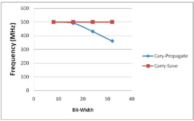
A two operand carry-propagate and conventional carry-save adder performances are compared first. As the bit-length of the operands increase, the performance of the carry-propagate addition is degraded. However, in carry-save format, the addition delay is not dependent on bit-lengths as seen in Fig. 6. As can be seen in Fig. 6., the carry-save format has the fastest frequency
response, not dependent on the bit length. The proposed double carry representation addition is accomplished in only a single LUT delay. However, conventional carry-save structure seen in Fig. 2.b. can be implemented using two levels of LUT cascades. Table 1 shows the LUT delays of various adder structures and required hardware.
A
B
C
D
Figure 7. Addition setup for four operands
For conventional carry-save structure, two levels of LUT delays always provides faster response, however, cascading more than two addition stages degrades the maximum performance. Fig. 7 shows a redundant addition scheme to add four redundant operands with redundant results.
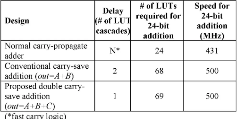
Table 1. Comparison of various addition schemes
Design Delay (# of LUT cascades) # of LUTs required for 24-bit addition Speed for 24-bit addition (MHz) Normal carry-propagate adder N* 24 431 Conventional carry-save 2 68 500 addition (out=A+B) 2 68 500
Proposed double
carry-save addition 1 69 500
(out=A+B+C)
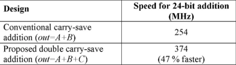
Table 2. Comparison of conventional carry-save and new carry-save structures according to the test setup
Design Speed for 24-bit addition
(MHz)
Conventional carry-save
addition (out=A+B) 254
Proposed double carry-save addition (out=A+B+C)
374 (47 % faster)
The performance of the addition shown in Fig.7, by using different techniques, is tabulated in Table 2. As conventional carry-save addition is made through two LUT stages, test setup seen in Fig.7 requires four LUT cascades. However, double carry-save representation reduces the addition stages and proposed carry-save representation provides 47 % speed improvement.
6. CONCLUSION
In this work, a new double carry-save addition architecture is proposed for 6-input LUT based FPGAs. The performance of the new circuit and the classical propagate and redundant save addition schemes are compared. The conventional carry-save addition structure completes addition process in two LUT delays, however, our proposed double carry-save format completes in a single 6-input LUT delay. The proposed addition scheme has shown 47 % faster performance, for four-operand addition, compared to normal carry-save. The proposed architecture can provide fast arithmetic especially for arithmetic architectures that require recursive addition operations such as convolution, matrix multiplication and similar digital arithmetic operations.
REFERENCES
[1] S. Brown and J. Rose, "FPGA and CPLD Architectures: A Tutorial", IEEE Design and Test of Computers, Vol. 12, No. 2, Summer 1996, pp. 42-57.
[2] Altera Stratix II Device Handbook (2009), www.altera.com [3] Xilinx Virtex-5 Family Overview(2009), www.xilinx.com [4] T. G. Noll, "Carry-Save Architectures for High-Speed Digital Signal Processing", Journal of VLSI Signal Processing, vol. 3, pp. 121-140, 1991.
[5] B. Parhami, "Generalized Signed-Digit Number A Systems: A Unifying Framework for Redundant Number Representations",
IEEE Trans. on Computers, Vol. 39, No: 1, Jan. 1990.
[6] I. Koren, "Constant-Time Addition and Simultaneous Format Conversion Based on Redundant Binary Representations", IEEE
Trans. On Computers, Vol. 50, No. 11, Nov. 2001
[7] M. D Ercegovac and T. Lang," Digital Arithmetic", Morgan Kauf mann, 2004.
[8] I. Koren, Computer Arithmetic Algorithms, AK Peters, 2002. [9] R. Zimmermann," Binary Adder Architectures for Cell Based VLSI and their Synthesis", PhD thesis, Swiss Federal Institute of Technology, Zurich, 1997.