First Results on Sensitivity, Dynamic Range and
Instantaneous Bandwidth Measurements
Ali Bugra Korucu, Yasar Kemal Alp, Gokhan Gok
Radar, Electronic Warfare and Intelligence Systems DivisionASELSAN A.S. Ankara, Turkey
{abkorucu,ykalp,ggok}@aselsan.com.tr
Orhan Arikan
Dept. of Electrical and Electronics Engineering Ihsan Dogramaci Bilkent University
Ankara, Turkey [email protected]
Abstract—In this work, sensitivity, one/two-signal dynamic range and instantaneous bandwidth measurement results of the recently developed Compressive Digital Receiver (CDR) hard-ware for Electronic Support Measures (ESM) applications, will be reported for the first time. Developed CDR is a compressive sens-ing based sub-Nyquist samplsens-ing receiver, which can monitor 2.25 GHz bandwidth instantaneously by using four ADCs (Analog-to-Digital Receiver) each of which has a sampling rate of 250 MHz. All the digital processing blocks of the CDR are implemented in Field Programmable Gate Array (FPGA) and they work in real time. It is observed that the sensitivity and dynamic range of the CDR changes with respect to input signal frequency. For 2.25 GHz bandwidth, the best and worst sensitivity values of the CDR are reported as -62 dBm and -41 dBm, respectively. One-signal dynamic range of CDR is measured as at least 60 dB for the whole band. The best and worst values of the two-signal dynamic rage values are observed as 42 dB and 20 dB, respectively.
Index Terms—compressive sensing, digital receiver, sub-Nyquist sampling, sensitivity, one/two-signal dynamic range, instantaneous bandwidth.
I. INTRODUCTION
With the recent developments in radar technology, the requirements of ESM systems have become harder. One of the most important requirements of an ESM system is the instantaneous bandwidth of its digital receiver [1]. In tradi-tional digital ESM receivers, the sampling rate of the ADC used defines its instantaneous bandwidth. In today’s most advanced ESM systems, ADC’s with sampling rate up to 3 GHz are used. Although this rate enables achieving an instantaneous bandwidth of 1.5 GHz in theory, in practical implementations at most 1 GHz bandwidth is obtained. Also, as the sampling rate of ADCs increase, their dynamic range (number of bits) decrease. Note that an ESM system typically requires at least 30 dB instantaneous dynamic range, which corresponds to at least 8 bit representation levels for the ADCs. Hence, new digital receiver technologies should be developed to achieve higher instantaneous bandwidths (>2 GHz) with lower sampling rates based on sub-Nyquist sampling methods. One of the most important sub-Nyquist sampling method-ologies is compressive sensing based architectures. In
liter-ature, many methods have been proposed for compressive sampling based sub-Nyquist sampling [2]–[4]. In all of these methods, although the proposed theory is very fluent and straight forward, no real data results have been shared. In [5], design of an RF (Radio Frequency) circuitry for implementing the analog compression method in [4] is detailed. However, implementation details of the recovery algorithm on a real hardware together with the real data results are omitted.
In this work, sensitivity, one/two-signal dynamic range and instantaneous bandwidth measurement results of the recently developed CDR hardware, which detects the radar pulses and measures their parameters such as TOA (time of arrival), PW (Pulse Width), amplitude, frequency etc., will be reported for the first time. The developed hardware is based on the MWC (Modulated Wideband Converter) technique given in [4], how-ever has a totally original RF and digital hardware design. Preliminary offline recovery results on real data acquired by the prototype hardware has been given in [6]. In this work, sensitivity, one/two-signal dynamic range and instantaneous bandwidth measurement results of the final hardware design will be shared.
CDR is mainly composed of two blocks: i)Analog Process-ing Block and ii) Digital ProcessProcess-ing Block. In the Analog Processing Block, incoming RF signal is compressed in the spectrum by using analog circuits. In the Digital Processing Block, the low bandwidth, compressed data is digitized by using four ADCs each of which sampling at 250 MHz rate. The recovery algorithm, OMP (Orthogonal Matching Pursuit), is utilized over the collected samples, where the total data rate is 1GHz. The Digital Processing Block has been fully implemented in FPGA and is running in real time. Conducted experiments show that, the developed CDR has an instanta-neous bandwidth of at least 2.25 GHz. Its sensitivity value changes with the input signal frequency where it is observed to be -62 dBm at best and -41 dBm at worst through out the 2.25 GHz bandwidth. The one-signal dynamic range is reported as at least 60 dB for the whole band. The two-signal dynamic range changes according to frequency and its best and worst values are reported as 45 dB and 20 dB along the
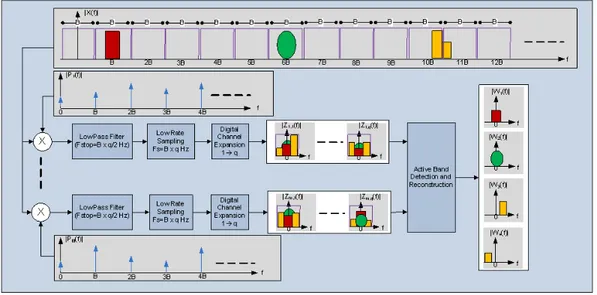
Fig. 1. Block schema of the Modulated Wideband Converter. 2.25GHz bandwidth, respectively.
The paper is planned as follows. In Section-II, the math-ematical background on Modulated Wideband Converter is given. The implementation details of CDR are provided in Section-III. The experiment results and resource allocation table of the FPGA implementation of the OMP are given in Section-IV. Finally, Section-V is reserved for conclusions.
II. MATHEMATICALBACKGROUND
Let F =[−FN yq/2, FN yq/2] be the operating frequency
range of the MWC system whose block diagram is given in Fig.1. Assume that this range has been divided into 2L+1 sub-bands of bandwidth B. Each sub-band has the following fre-quency support Fl=[lB−B/2, lB+B/2], l=−L, .., L, where
the first and the last sub-bands satisfy the following conditions −LB−B/2≥−FN yq/2 and LB+B/2≤FN yq/2, respectively.
Consider the following multi-band measurement model, which has P active bands:
x(t) =
P
X
p=1
ap(t)ej2πBlpt. (1)
Here lp∈[−L, L] and ap(t) is the complex bandlimited signal
satisfying Ap(f )=0, ∀|f |≥B/2, where Ap(f ) is the Fourier
transform of ap(t) defined as Ap(f ) =
R∞
−∞ap(t)e
−j2πf tdt.
Once x(t) is received by the MWC, it is divided and fed into M identical analog channels, where in each chan-nel x(t) is multiplied by the real and periodic waveforms pm(t), m=1, .., M . These waveforms are different from each
other but they have the same period Tp = 1/B. Hence, each
waveform have the following Fourier series expansion: pm(t) =
∞
X
k=−∞
cm,kej2πkBt, (2)
where cm,k is the kth Fourier series coefficient
of the mth waveform, which can be computed as
cm,k=B
Rt0+1/B
t0 pm(t)e
−j2πkBtdt for any time instant t 0.
Note that cm,k=c∗m,k, since pm(t) is real. The representative
spectra of pm(t) are shown as Pm(f ) in Fig.1. In each analog
channel, before the analog low-pass filter the following signal appears: ym(t) = x(t)pm(t) = ∞ X k=−∞ P X p=1 cm,−lp+kap(t)e j2πkBt . (3) If the stop band frequency of the identical analog low-pass filters in each channel is chosen as q×B/2, where q being the channel expansion factor [4], the resulting signals vm(t) at the
end of each filter can be written as: vm(t) = ˆ q X k=−ˆq P X p=1 cm,−lp+kap(t)e j2πkBt, (4) where ˆq=(q−1)/2. Note that analog filters are assumed to be ideal to simplify the formulation.
Vm(f ) = ˆ q X k=−ˆq P X p=1 cm,−lp+kAp(f + kB), (5)
where Vm(f ) is the Fourier transforms of vm(t) respectively.
Note that different linear combinations of ap(t), p=1, .., P
signals appear at centre frequencies kB, k=−ˆq, .., ˆq in vm(t).
To expand the number of channels by a factor of q, each channel is sampled at a rate Fs≥qB and multiplied by
ej2πq0Bn/Fs, q0=−ˆq, .., ˆq and a digital low-pass filter with
cut-off frequency B/2 is applied. Hence, from each analog channel, the following q digital sub-band channel signals are generated:
vm,q0[n] = (vm(nTs)ej2πq 0BnT
s), q0=−ˆq, .., ˆq, (6)
where Ts = 1/Fs is the sampling period of the ADC.
Similar to analog filtres, digital low-pass filters are assumed to have ideal responses to simplify the formulation. (6) can be equivalently written in the spectral domain as:
Vm,q0(f ) =
P
X
p=1
cm,−ln+q0Ap(f ), |f | ≤ Fs/2. (7)
Here Vm,q0(f ) is the Fourier transform of the digital signal
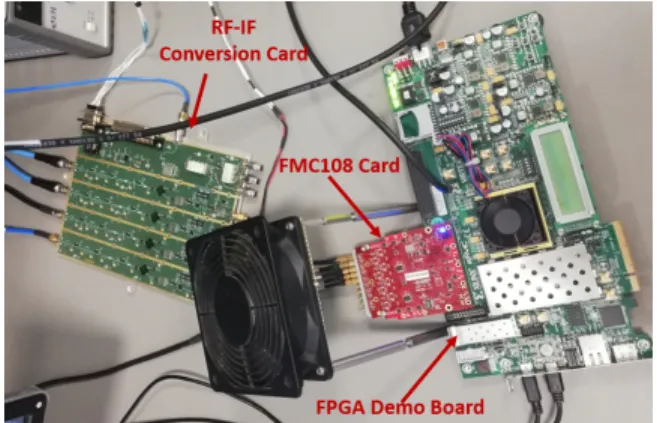
Fig. 2. RF-IF conversion card of the CDR.
analog channel. All the M × q channels have identical fre-quency response hence (7) can be written as the following linear system of equations:
v(f ) = Cb(f ) (8) where CM q×2L+1= c1,−L−ˆq c1,−L+1−ˆq .. c1,L−ˆq c1,−L−ˆq+1 c1,−L+1−ˆq+1 .. c1,L−ˆq+1 . . .. . c1,−L+ˆq c1,−L+1+ˆq .. c1,L+ˆq c2,−L−ˆq c2,−L+1−ˆq .. c2,L−ˆq . . .. . . . .. . cM,−L+ˆq cM,−L+1+ˆq .. cM,L+ˆq , vM q×1(f ) = V1,−ˆq(f ) V1,−ˆq+1(f ) . V1,ˆq(f ) V2,−ˆq(f ) . . VM,ˆq(f ) , b2L+1×1(f ) = b1(f ) b2(f ) . . b2L+1(f ) , (9) b(f ) is P -sparse, with the following non-zero entries blp+L+1(f )=Ap(f ), p=1, .., P . For the discrete set of
fre-quency values fn, n = 0, 1, .., N − 1, where fn = Fsn/N ,
a multiple measurement formulation of (8) can be constructed as:
V = CB, (10)
where V=[v(f0), .., v(fN −1)] and B=[b(f0), .., b(fN −1)].
Given the multiple measurement vector V and the system matrix C, the sparsest (block sparsity) B satisfying (10) is to be found. There are many fast greedy algorithms for solving (10) [7], [8]. Note that, by multiplying both sides of (10) with the inverse DFT matrix from the right, would enable to work with time domain samples rather than the spectral slices.
III. HARDWAREIMPLEMENTATION
Developed CDR has two main components: i)Analog Pro-cessing Block and ii)Digital ProPro-cessing Block. The first
Fig. 3. CDR setup.
component is the RF (Radio Frequency)-IF (Intermediate Frequency) conversion hardware. The second component is a FPGA (Field Programmable Gate Array) demo board, on which the compressed data is digitized and real-time recon-struction is applied to the generated samples. Randomization waveforms are generated using a Arbitrary Waveform Gener-ator, where the subband bandwidth is set to 25MHz.
A. Analog Processing Block
Analog processing block is actually an RF-IF conversion card. A picture of this card is given in Fig 2. This card has one RF signal input port, four LO (Local Oscillator) signal input ports and four IF signal output ports. There are also control interfaces. The input RF signal is divided in to four identical channels. Each channel is composed of filters, attenuators, amplifiers, test points, etc. Once the RF signals on every channel are passed through this RF strip, they are mixed with the corresponding randomization waveforms (pm(t)) coming
from the LO ports of the card. On the LO path of each channel, there are multiple equalizers for balancing powers of the harmonics of the LO signals, appearing at every 25 MHz. On the mixer outputs, there are low- pass filters with stop band frequency of 125 MHz and digitally controllable attenuators and amplifiers to tune the amplitude level of the IF signal to be sampled by the ADC (Analogue-to-Digital) without being saturated. At the end of each analog channel, a spectrally compressed IF signal of bandwidth 125 MHz is generated. These signals are to be digitized and further processed by the Digital Processing Block, which will be detailed next. B. Digital Processing Block
Digital Processing Block is composed of a balcony card which includes 4 ADCs operating at 250MHz sampling rate and 16 bit resolution, and KCU105 FPGA Demo Board. The balcony card is plugged to the demo board. Four IF outputs of the Analog Processing Block are connected to the inputs of balcony card. Generated samples are transferred to the FPGA for processing. CDR setup is shown in Fig. 3. To increase the number of digital channels, as discussed in Section-II, frequency translation and low pass filtering are applied digitally. Hence, the number of the digital channels are increased to 24, each of which has a data rate of 30.25 MHz
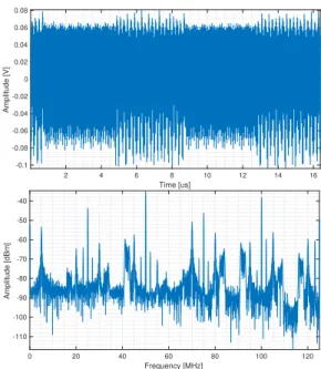
2 4 6 8 10 12 14 16 Time [us] -0.1 -0.08 -0.06 -0.04 -0.02 0 0.02 0.04 0.06 0.08 Amplitude [V] 0 20 40 60 80 100 120 Frequency [MHz] -110 -100 -90 -80 -70 -60 -50 -40 Amplitude [dBm]
Fig. 4. Compressed data from the first ADC (top) and its spectrum (bottom). and caries a complex data. Then, OMP algorithm implemented on FPGA is deployed that solves the linear system of equations given in (10) for reconstruction.
IV. EXPERIMENTALRESULTS
For measuring the instantaneous bandwidth, one/two signal dynamic range and sensitivity values of the CDR, first online system calibration procedure detailed in [9] is deployed and the system matrix C given in (10) has been filled.
For the instantaneous bandwidth measurement, RF output of three signal generators have been combined with a power combiner. Output of the power combiner has been connected to the RF input of the CDR. The signal generators have been ad-justed such that the following waveforms are generated: i) CW (Continuous Wave) signal with center frequency 258 MHz, amplitude -35 dBm, FM (Frequency Modulation) bandwidth 2 MHz and FM rate 2 kHz; ii)CW signal with center frequency 2502 MHz, amplitude -25 dBm; iii) Pulse signal with center frequency 1505MHz, amplitude -30 dBm, pulse width 4 us and pulse repetition interval 8 us. Note that since two of the generated signals are CW, when the pulse signal is active, thee signals overlap in time, which is a very rare situation in a typical EW scenario. By choosing the center frequencies of the signals as 258 MHz, 1505 MHz and 2502 MHz, we aimed to validate that the CDR has an instantaneous bandwidth of at least 2250 MHz. All the data acquisition and recovery processes have been utilized in FPGA and they work in real time. To demonstrate the results, the acquired compressed data and the recovered baseband signals for 16us interval have been transferred to the computer from the Ethernet connection of the FPGA demoboard. The acquired compressed data from the first ADC and the corresponding spectrum are shown in Fig. 4. As observed the measured compressed signal is highly aliased, very complicated and it is very hard to recognize the waveforms coming from the signal generators. The recovery
2 4 6 8 10 12 14 Time [us] -0.3 -0.2 -0.1 0 0.1 0.2 0.3 Amplitude [V] -15 -10 -5 0 5 10 15 Frequency [MHz] -70 -60 -50 -40 -30 -20 Amplitude [dBm]
Fig. 5. Recovered baseband signals (top) and their corresponding spectrum (bottom).
algorithm has detected 3 sub-bands with center frequencies 250 MHz, 1500 MHz and 2500 MHz for each sample. The recovered baseband signals, which are grouped based on their detected center frequencies, and their corresponding spectrum are plotted in Fig. 5. As observed baseband signals of all three waveforms together with their centre frequencies have been recovered successfully.
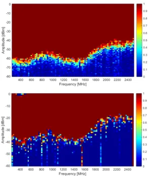
For measuring the sensitivity level of the CDR, a single signal generator has been connected to the RF input of the CDR. The signal generator parameters have been adjusted such that a CW signal is generated. The center frequency of the signal has been swept from 253 MHz to 2503 MHz with 25 MHz step sizes. For each frequency values, the amplitude level of the signal has been swept from -80 dBm to 0 dBm with 1 dB step sizes. For each frequency and amplitude pair, the real time recovery results of the approximately 10 us data (300 revored data sample) have been transferred to the computer. The probability of correct recovery for each amplitude-frequency pair is computed by dividing the number of correct centre frequency recoveries by 300. The resulting probability of correct recovery performance of the CDR as function of input signal frequency and amplitude level is shown in Fig. 6 on the top. The sensitivity curve of the CDR can be constructed by finding the minimum amplitude level for which the probability of correct recovery is higher than 0.99 for each frequency value. As observed, the sensitivity value of the CDR changes with respect to the frequency and has best and worst values of -62 dBm and -41 dBm through out the 2250 MHz bandwidth, respectively.
For two signal dynamic range measurement, RF output of two signal generators are combined using a power combiner and injected into to the CDR. From the first signal generator, a CW signal with fixed center frequency 2508 MHz and amplitude level 0 dBM has been given. The frequency and the amplitude level of the CW signal given from the second signal
Fig. 6. Probability of correct recovery graphs for the sensitivity (top) and two-signal dynamic range measurements(bottom).
generator has been swept from 256MHz to 250 6MHz with 25 MHz step size and from -60 dBm to 0 dBm with 1 dB step size, respectively. Similar to sensitivity test, for each frequency-amplitude pair of the second signal, an approximately 10 us data has been acquired, the probability of correct recovery is computed based on the recovery results. Note that correct recovery in this test is defined as the successful recovery of the subband indices of both signals. Obtained probability of correct recovery graph as a function of frequency and amplitude level of the second signal is shown in Fig. 6, on the bottom. As observed, two-signal instantaneous dynamic range value of the CDR has best and worst values of 42 dB and 20 dB through out the 2250MHz bandwidth, respectively. All the polyphase filtering and recovery processes are running in real time on the FPGA. The clock frequency of the FPGA is 250MHz. Polyphase filtering operation which generates 24 digital sub-band channels at a rate of 30.25 MHz each, is straight forward. On the other side, the implementation of OMP algorithm in FPGA is very complicated since the algorithm is iterative and requires computation of matrix inverses in each iteration. By optimizing the OMP algorithm for memory/computational resource usage and utilizing some simplifications on the algorithm (applying matrix inversion lemma, binomial series expansion for avoiding fixed point di-visions, etc.), the algorithm has been successfully implemented on FPGA. For each acquired sample, the algorithm runs for 3 iterations (for recovering maximum 3 signals), where in the last iteration inverse of a 6x6 matrix is computed. The details of the OMP implementation on FPGA are given in [10]. The FPGA resource utilization in terms of number of LUTs (Look Up Table), FFs (Flip Flops), DSPs (Digital Signal Processing Element) and BRAMs (Block Ram) used are given in Table
(K) (K) (36K1) Freq.(MHz) (ns) (dBFS) M = 24, N = 10 22.8 22.0 392 85.5 216.7 941.5 -75.6 M = 24, N = 50 59.9 41.2 914 185.5 216.7 941.5 -75.6 M = 24, N = 100 106.9 65.1 1562 310.5 216.7 941.5 -75.6 M = 24, N = 10 24.0 24.1 392 85.5 216.7 941.5 -81.7 M = 24, N = 50 62.3 43.7 914 185.5 216.7 941.5 -81.7 M = 24, N = 100 110.3 68.3 1562 310.5 216.7 941.5 -81.7 1. In the table, M and N represent the size of the complex dictionary C. The first three and the last three rows show the obtained results for carrying 16 bit and 18 bit fixed point arithmetic operations in FPGA, respectively. The Max Clock Frequency and Latency columns represent the maximum clock frequency achived and the resulting latency for the given M, N values, respectively. The last column MSE (Mean Square Error), displays the error between recovery results obtained from fixed point FPGA recovery and the double precision computer recovery. Using 18bit fixed point arithmetic provides better MSEs, as expected.
V. CONCLUSIONS
In this work, sensitivity, one/two-signal dynamic range and instantaneous bandwidth measurement results of the recently developed Compressive Digital Receiver (CDR) hardware for Electronic Support Measures (ESM) applications, is reported for the first time. The developed CDR has its own RF-IF conversion card. The digital processing part has been carried on a FPGA demo board. All the digital processing including real time recovery has been implemented in FPGA. The obtained results show that the developed hardware can be effectively used in an ESM system as a digital receiver.
REFERENCES
[1] R. G. Wiley, “Electronic Intelligence: The Interception of Radar Sig-nals”, Artech House, 1985.
[2] J. A. Tropp, M. F. Duarte, J. K. Romberg, R. G. Baraniuk, “Beyond Nyquist: Efficient Sampling of Sparse Bandlimited Signals” IEEE Trans. Inf. Theory, vol. 56, pp. 520-544, 2010.
[3] M. Lexa, M. E. Davies, J. Thompson, “Multi-coset Sampling and Recovery of Sparse Multiband Signals”, Tech. Report, 2010.
[4] M. Mishali and Y. Eldar, “From Theory to Practice: Sub-Nyquist Sam-pling of Sparse Wideband Analog Signals”, IEEE Journal of Selected Topics in Signal Processing, vol. 4, no. 2, 2010.
[5] M. Mishali, Y. Eldar, O. Dounaevsky, E. Shoshan “Xampling: Analog to digital at sub-Nyquist rates”, IET Circuits, Devises & Systems, vol. 5, no. 1, 2011.
[6] A. B. Korucu, O. Cakar, Y. K. Alp, G. Gok, O. Arikan, “Compressed Digital Receiver: First Hardware Implementation Results,” SIU 2018, esme, Turkey.
[7] S. Cotter, B. Rao, K. Engan, K. Delgado, “Sparse Solutions to Linear Inverse Problems With Multiple Measurement Vectors,” IEEE Transac-tions on Signal Processing, vol. 53, no. 7, 2005.
[8] J. Tropp, A. Gilbert, “Simultaneous Greedy Approximations via Greedy Pursuit,” ICASSP 2005.
[9] Y. K. Alp, A. B. Korucu, A. T. Karabacak, A. C. Gurbuz, O. Arikan, On-line Calibration of Modulated Wideband Converter, SIU 2016, Karabuk, Turkey
[10] A. B Korucu, O. Cakar, Y. K. Alp, G. Gok, O. Arikan “Compressive digital receiver: FPGA Implementation of OMP Algoritm”, SIU 2019, Sivas, Turkey.