DESIGN, FABRICATION, AND
APPLICATIONS OF MULTI-MODE
NANOELECTROMECHANICAL SYSTEMS
a thesis submitted to
the graduate school of engineering and science
of bilkent university
in partial fulfillment of the requirements for
the degree of
master of science
in
mechanical engineering
By
Atakan Bekir Arı
July 2017
DESIGN, FABRICATION, AND APPLICATIONS OF MULTI-MODE NANOELECTROMECHANICAL SYSTEMS
By Atakan Bekir Arı July 2017
We certify that we have read this thesis and that in our opinion it is fully adequate, in scope and in quality, as a thesis for the degree of Master of Science.
Mehmet Selim Hanay(Advisor)
Haluk K¨ulah
Onur ¨Ozcan
Approved for the Graduate School of Engineering and Science:
Ezhan Karasan
ABSTRACT
DESIGN, FABRICATION, AND APPLICATIONS OF
MULTI-MODE NANOELECTROMECHANICAL
SYSTEMS
Atakan Bekir Arı
M.S. in Mechanical Engineering Advisor: Mehmet Selim Hanay
July 2017
Miniaturization of systems allowed wide spread consumer use of microelectron-ics, integrated circuits and MEMS based sensors. Thanks to the advancement in microfabrication methods, it is possible to build structures with submicron dimen-sions. The integration of electronic control to these submicron structures started the NEMS field. Due to their minuscule dimensions and very high frequency re-sponse, NEMS can sense external perturbations with unprecedented sensitivity. This made NEMS excellent candidates for sensor applications. NEMS are start-ing to evolve from academic research tools to become mass produced and large scale integrated sensing devices.
Information extracted from the higher order modes further increase the capa-bilities of NEMS. In order to attain this extra information, we fabricated NEMS that can reach higher order mechanical modes. Every step of fabrication was done at Bilkent University research facilities such as UNAM and ARL. To pattern the submicron feature sizes, we relied on electron beam lithography. Thermal and electron beam evaporators were deployed for metallization of contacts and etch mask. In order to suspend the doubly clamped beams, we developed anisotropic silicon nitride and isotropic silicon dry etch recipes. At each step of the fabrica-tion, tools such as SEM and stylus profilometer was utilized for characterization. Fabricated NEMS were wirebonded to printed circuit boards for detection.
Electrothermal actuation, an integrated method, was chosen to drive the nanomechanical resonator to its higher order modes. Piezoresistive down-mixing, another integrated method to complement the actuation, was used to detect the resulting nanomechanical motion. We used high frequency electronic equipment
iv
to detect RF range responses of our NEMS. Using these NEMS, we studied two novel applications on intermodal and mechanical coupling.
First, we investigated intermodal coupling effect of doubly clamped beams in order utilize this coupling effect in higher order mode detection. When a doubly clamped beam is excited at its resonance frequency, every other mode of the device gets tuned. This occurs due to the clamping on both sides preventing longitudinal elongation and causing a stress on the beam. Using intermodal coupling method, we probed higher order modes of a nanomechanical resonator while tracking the fundamental frequency at the same time. We were able to detect mechanical modes up to 840 MHz, well out of the detection limit of our setup. We propose intermodal coupling as a novel detection method to acquire frequency response of NEMS at higher order modes which can not be detected with conventional methods.
Finally, we studied nano scale energy sinks that absorb energy from a another structure. Energy sinks are linear oscillators that can trap the energy of a nearby structure within their phase space. When the natural frequency of these sinks are distributed optimally, finite number of sinks can mimic absorption of infinite sinks. We envisioned a real time dissipation controlled NEMS platform by de-ploying energy sinks. In order to test energy sink performance at nano scale, we devised an experimental setup, comparing identical nanomechanical resonators with and without energy sinks. We have shown that energy sinks successfully absorb energy of a resonator at nanoscale.
Keywords: NEMS, Nanofabrication, Electron Beam Lithography, Reactive Ion Etching, Electrothermal Actuation, Piezoresistive Down-Mixing, Nanomechanics, Mode-Coupling, Energy Sinks, Quality Factor Modulation.
¨
OZET
C
¸ OK MODLU NANOELEKTROMEKAN˙IK
S˙ISTEMLER˙IN TASARIM, ¨
URET˙IM, VE
UYGULAMALARI
Atakan Bekir Arı
Makine M¨uhendisli˘gi, Y¨uksek Lisans Tez Danı¸smanı: Mehmet Selim Hanay
Temmuz 2017
Sistemlerin minyat¨urle¸stirilmesi ile birlikte mikroelektronik, entegre de-vre, ve MEMS bazlı sensorler geni¸s marketlere a¸cılabildi. Mikrofabrikasyon tekniklerindeki geli¸smeler sayesinde artık bir mikrondan daha k¨u¸c¨uk boyutlu yapılar ¨uretilebiliyor. Bu yapıların elektronik cihazlarla kontrol¨u NEMS alanının ba¸slamasına sebep olmu¸stur. NEMS, ¸cok k¨u¸c¨uk boyutları ve y¨uksek frekanslı tep-kileri sayelerinde harici uyarıları rakipsiz bir hassaslıkla ¨ol¸cebilir. Bu ¨ozellikler sayesinde NEMS, sensor uygulamaları i¸cin m¨ukemmel bir se¸cenektir. G¨un¨um¨uzde NEMS, akademik ara¸stırma ara¸cları olmaktan ¸cıkıp seri imalat ile ¨uretilip geni¸s ¨
ol¸cekte t¨umle¸sen cihazlar haline geliyor.
Y¨uksek modlardan elde edilen bilgi NEMS0lerin kabiliyetlerini olduk¸ca arttırıyor. Bu sebeple, y¨uksek mod uygulamalarında kullanılmak ¨uzere bu mod-lara ula¸sabilen NEMS ¨urettik. Bu cihazların ¨uretimi, UNAM ve ARL gibi Bilkent ¨Universitesi ara¸stırma laboratuvarlarında ger¸cekle¸stirildi. Mikrondan k¨u¸c¨uk yapıların ¨uretimi i¸cin elektron demeti litografisinden yararlandık. Ter-mal ve elektron demeti eriticileri ise metalizasyon a¸saTer-malarında kullanıldı. C¸ ift ankastreli yapıların serbest bırakılması ise anisotropik silikon nitrat ve isotropik silikon kuru a¸sındırma teknikleriyle ger¸cekle¸stirildi. ¨Uretimin her adımında SEM ve profilometre ile niteleme yapıldı. ¨Uretimi tamamlanan cihazlar ¨ol¸c¨umler i¸cin baskılı devre kartlarına tutturuldu.
T¨umle¸sik bir teknik olan elektrotermal s¨urme NEMS0leri y¨uksek modlara s¨urmek i¸cin kullanıldı. Olu¸san nanomekanik hareketlerin ¨ol¸c¨um¨u ise piezorezistif frekans-a¸sa˘gı-kaydırma ile yapıldı. ¨Ol¸c¨umleri y¨uksek frekanslı elektronik ekipman ile yaptık. Bu NEMS0leri kullanarak iki yeni uygulama ¨uzerinde ¸calı¸sma yaptık.
vi
˙Ilk olarak, modlar arası e¸sle¸sme etkisini y¨uksek modlarda kullanmak ¨uzere ¸cift ankastreli kiri¸sler ¨uzerinde ¸calı¸stık. C¸ ift ankastreli bir kiri¸s resonans frekansında s¨ur¨uld¨u˘g¨u zaman di˘ger b¨ut¨un modları de˘gi¸sime u˘grar. Bu etkinin sebepi ¸cift ankastreli yapının kiri¸sin uzamasını engelleyerek kiri¸s ¨uzerine bir gerilim uygu-lamasıdır. Bu modlar arası e¸sle¸sme metodunu kullanarak, bir nanomekanik res-onat¨or¨u do˘gal frekansında s¨urerken, y¨uksek modlarını sırasıyla yokladık. ¨Ol¸c¨um ekipmanımızın limitinin ¸cok ¨ust¨unde olan 840 MHz0e kadar mekanik mod ¨ol¸c¨um¨u yapmayı ba¸sardık. Modlar arası e¸sle¸sme metodunu ¨ol¸c¨um¨u zor olan y¨uksek mod-ların ¨ol¸c¨um¨u i¸cin yeni bir ara¸c olarak sunuyoruz.
Son olarak, yapıların enerjisini emen enerji s¨on¨umleyicileri nano boyuta adapte ettik. Enerji s¨on¨umleyiciler yakınlarındaki yapıların enerjilerini kendi faz uzay-larında hapsedebilen lineer osilat¨orlerdir. Bu enerji s¨on¨umleyicilerin frekansları optimum bir ¸sekilde d¨uzenlendi˘ginde sonsuz sayıdaki s¨on¨umleyicinin etkisini sonlu sayıda s¨on¨umleyici ile taklit edebiliriz. Bu cihazları kullanarak ger¸cek za-manlı enerji kaybı kontrol¨u yapalabilen bir NEMS platformu tasavvur ettik. Bu yapıları test etmek amacıyla deneysel bir d¨uzenek kurduk. Enerji s¨on¨umleyicili ve enerji s¨on¨umleyicisiz NEMS0leri kar¸sıla¸stırarak enerji s¨on¨umleyicilerin nano boyutta enerji kaybı kontrol¨u i¸cin kullanılabilece˘gini g¨osterdik.
Anahtar s¨ozc¨ukler : NEMS, Nanofabrikasyon, Elektron I¸sını Litografisi, Reak-tif ˙Iyon A¸sındırma, Elektrothermal S¨ur¨um, Piezorezistif frekans-a¸sa˘gı-kaydırma, Nanomekanik, Mod E¸sle¸sme, Enerji S¨on¨umleyici, Q Fakt¨or¨u Mod¨ulasyonu.
Acknowledgement
First of all, I would like to thank my MS thesis advisor M. Selim Hanay for his guidance and generous support during my graduate study. It wouldn’t be an exaggeration if I said meeting Dr. Hanay changed my life completely. His work altered my view of mechanical engineering and he inspired me to become a better engineer and a scientist. It is a great honor for me to be one of his first graduate students.
I would like to thank my MS thesis committee, Prof. Onur ¨Ozcan and Prof. Haluk K¨ulah for their time and valuable suggestions. I’m grateful to Dr. Cenk Yanık for all his help and invaluable tips on fabrication and e-beam lithography. I want to thank Prof. Kamil Ekinci for all the discussions and for our work together. I learned a lot from him during our time in Bilkent and Boston University. Ahmet can Kırlıo˘glu, Vural Kara, Josh Javor, and Pınar Karayaylalı; thank you for making my brief time in Boston memorable. Pınar, thank you for being there for me during the hardest times and lend an ear whenever I needed to vent.
I want to thank my brilliant colleagues Mustafa C¸ a˘gatay Karakan, Sel¸cuk O˘guz Erbil, Ezgi Orhan, Hande Aydo˘gmu¸s, Mehmet Kelleci, Levent Aslanba¸s, and Mert Y¨uksel from Hanay Research Group. It was my privilege to share the lab and a part of my life with you. Thank you all for your support and friendship. C¸ a˘gatay, you have been one of my best friends for a very long time now. I’m glad we got to work together in graduate school and I’m glad we will continue to do so. Sel¸cuk, you are one of the few people whom I would trust with my NEMS; thank you for your selfless support and help during fabrication.
I have shared the hardships of graduate school with a lot of amazing people here in Bilkent University Mechanical Engineering Department. Anıl Alan, Bu˘gra T¨ureyen, Arda Balkancı, Serdar Taze, Hossein Alijani, Negin Musavi, Alper
¨
Ozo˘gul, M¨uge ¨Ozcan, and even though not technically a grad student Furkan Ayhan; thank you all for your friendship and for all the thoughtful discussions
viii
we had. I want to thank our administrative assistant Ela ¨Ozsoy for bearing with my most ridiculous requests all these years from undergrad to graduate school.
As an important part of this MS study was spent in the cleanroom, I want to thank staff and personnel of UNAM and ARL. Especially Murat G¨ure, Mustafa G¨uler, Hakan S¨urel, Semih Bozkurt, Abdullah Kafadenk. Thank you for keep-ing everythkeep-ing runnkeep-ing and ready. Without your expertise on microfabrication I wouldn’t be able to fabricate NEMS at Bilkent University. I’d like to also acknowledge Ufuk Turan’s help with the fabrication of the printed circuit boards.
Finally, I would like to express my gratitude to my family. My dear brothers Hakan and Sinan, thank you for being there for me whenever I needed and giving me strength to go on no matter what. Mom and Dad, thank you for believing me and pushing me to become a better person. Your unconditional love and support made me what I am today. Everything I aspire to be, I owe it to you.
We acknowledge support from T ¨UB˙ITAK (grant number 113E600) for part of the work presented here.
Contents
1 Introduction 1
1.1 Nanoelectromechanical Systems . . . 2
1.2 Flexural Vibrations of Doubly Clamped Beams . . . 3
1.3 Thesis Outline . . . 6
2 Fabrication Methods for NEMS 8 2.1 Design . . . 9
2.1.1 Design Rationale . . . 10
2.2 Sample Preparation . . . 11
2.3 Lithography . . . 14
2.3.1 Photolithography . . . 14
2.3.2 Electron Beam Photolithography . . . 18
CONTENTS x
2.4.1 Thermal Evaporation . . . 26
2.4.2 Electron Beam Evaporation . . . 29
2.5 Lift-off . . . 29 2.6 Etching . . . 32 2.6.1 Wet Etching . . . 32 2.6.2 Dry Etching . . . 33 2.7 Wirebonding . . . 38 2.8 Characterization . . . 39 2.8.1 Microscopy . . . 40 2.8.2 Profilometer . . . 41 2.8.3 Probe Station . . . 42
2.9 Fabrication Steps of Silicon Nitride Devices . . . 43
3 Transducers for NEMS 45 3.1 Electrothermal Actuation . . . 46
3.2 Piezoresistive Detection . . . 47
3.3 Detection Setup . . . 49
4 Applications 52 4.1 Intermodal Coupling Detection for Higher Order Nanomechanical Modes . . . 52
CONTENTS xi
4.2 Nanomechanical Resonator Platform with Tunable Quality Factor 62
5 Conclusion and Future Work 68
A RCA Clean 79
List of Figures
1.1 Two examples of NEMS devices fabricated during this study with widths and thicknesses smaller than a micrometer. . . 3
1.2 A doubly clamped beam with length L, width w and thickness t. . 4
1.3 Mode shapes of a doubly clamped beam for n=1,2,3,4. . . 5
2.1 A multi layered GDSII design . . . 10
2.2 GDSII design of contact pads (a) patterned onto a 5 inch soda lime photomask (b) by a mask writer. . . 15
2.3 Exposure Process and effect of UV radiation on positive resist (a) and negative resist (b). . . 17
2.4 Dose factors for the same design. (a) has no proximity correction while (b) is proximity corrected. . . 20
2.5 Dose test characterization by SEM. . . 22
2.6 SEM image of a NEMS device that had gone through 2 alignment procedures. . . 24
LIST OF FIGURES xiii
2.8 Few example of boats and crucibles used for evaporation. . . 27
2.9 Inside of a thermal evaporator chamber. . . 28
2.10 Inside of an e-beam evaporator chamber. . . 30
2.11 Lift-off mechanism. . . 31
2.12 Unsuccessful lift-off procedures. . . 32
2.13 Stiction of a silicon beam after HF based oxide wet etch. . . 33
2.14 Schematic of an ICP chamber. . . 35
2.15 Etch recipe development steps. . . 38
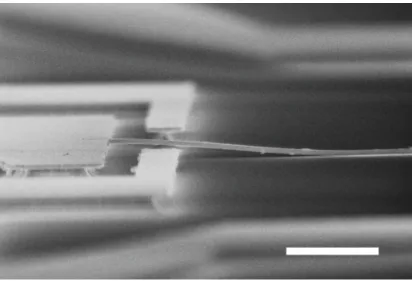
2.16 Photograph of a wirebonder during bonding operation (a). SEM micrograph of a wirebonded device (b). . . 39
2.17 A silicon chip with dozens of NEMS, wirebonded to a 5 port printed circuit board. . . 40
2.18 Images of a NEMS taken with optic microscopy (a), SEM (b) and tilted view with SEM (c). . . 41
2.19 Stylus profilometer measurements of sample undergone a 100 cycle DRIE etch showing µm deep trenches. . . 42
2.20 Fabrication steps of silicon nitride devices - part A . . . 43
2.21 Fabrication steps of silicon nitride devices - part B . . . 44
3.1 AC (a) and DC operation (b) schematics of electrothermal actuation. 47 3.2 DC biasing (a) and AC biasing(c) for signal down-mixing . . . 48
LIST OF FIGURES xiv
3.3 Simplified Dbox architecture (a) and its connections to a typical NEMS device. . . 49
3.4 Mechanical response of a NEMS around 74.8 MHz detected using Dbox. . . 50
3.5 Comparison of the response of one of the first iteration of devices 50
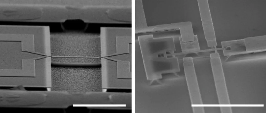
4.1 Scanning electron micrograph of a nanomechanical resonator . . . 53
4.2 Resonant response for the 1st mode at 20 mT orr . . . 54
4.3 Closed loop intermodal coupling measurements between 1st mode
and higher order modes . . . 55
4.4 A similar NEMS fabricated at Sabanci University as a colloboration. 57
4.5 Open loop measurement from 1 to 50 MHz in air . . . 58
4.6 Closed-loop intermodal coupling measurements using the first three out-of-plane modes. . . 58
4.7 PLL mode-coupling measurements between 1st and 2nd mode . . . 60
4.8 Macro scale (a) model versus nano scale (b) model of energy sink interaction. . . 63
4.9 Resonance frequency vs. energy sink length . . . 64
4.10 Top and tilted view SEM images of a NEMS with frequency dis-tributed energy sinks. . . 65
4.11 Detection scheme of the devices and first fundamental mode driven to nonlinearity. . . 65
List of Tables
1.1 Higher order solutions of a doubly clamped beam. . . 5
2.1 PMMA bilayer spin coating recipe for 300 nm thick film. . . 19
2.2 PMMA development procedure. . . 21
2.3 Etch recipes developed for silicon nitride and silicon for STS ICP. 37
4.1 Quality Factors of the first 5 modes and two ultra-high frequency 59
4.2 Features observed during the PLL on first and second mode, rang-ing from 40 to 150 MHz. . . 61
Chapter 1
Introduction
First electronic computers were as big as rooms, weighed dozens of tons, and re-quired thousands of watts to operate them back in 1940s; whereas today, we can fit a “computer” that has more computational power than the Apollo 11 ground computers had when they put a man on the moon. These pocket computers also have numerous sensors in them: accelerometers, gyroscopes, proximity sen-sors, barometers, GPS trackers and many more wondrous small machines. The widespread availability of such technology can be attributed to the miniaturiza-tion of systems which have been going on with an astonishing pace starting with the rise of the integrated circuit (IC) industry during the 1960s. We are trying to fit more and more into smaller and smaller spaces ever since.
This miniaturization effort of course brings challenges with it. Foreseen or completely unexpected obstacles arise at smaller scales. Even though the laws of physics do not change fundamentally; dominant forces do. Surface tension and capillary forces start to become prevalent over gravitational forces. Effectiveness of actuators and batteries diminishes as surface to volume ratio increases and so on. On the other hand, the incentives to scale down are enticing. There are economic reasons of course: smaller things require less materials to build, less energy to power which decreases the costs altogether. From a scientific standpoint however, small scale allows us to breakdown macro laws in physics and chemistry
allowing development of new paradigms.
Following the developments in IC industry and microfabrication methods, elec-tronically controlled micro scaled mechanical machines were built and were clas-sified as microelectromechanical systems [1]. MEMS field was a great success and quickly dominated the consumer electronics market with inkjet printers, ac-celerometers, electronic filters any many other sensor applications. Yet, as Feyn-man said there is still “plenty of room at the bottom” [2]. Thus, we moved on to the next big thing, or rather the small thing, ahead: nanoelectromechanical systems.
This thesis is a result of a work that hoped to protrude a tiny dent in the vast research field of NEMS. First and foremost goal was to fabricate functional NEMS at Bilkent University; specifically, NEMS that can reach higher order modes deep in to the microwave range. In order to achieve this goal we relied on the cleanroom and microfabrication capabilities of National Nanotechnology Research Center (UNAM) which is located in Bilkent University Campus. Second part of this study was to use these “homemade” NEMS for multi-mode sensing applications where information extracted from such modes would be utilized.
1.1
Nanoelectromechanical Systems
NEMS are electronically controlled mechanical machines with at least one dimen-sion smaller than a micrometer. They can be considered as even smaller MEMS. Starting with first demonstrations in 1996 [3], NEMS field grew rapidly and has been very active. Due to their nanoscale dimensions, NEMS offer interesting capabilities such as: resonance frequencies in microwave range [4], Quality (Q) factors in the tens of thousands [5], heat capacities below yoctocalories [6], effec-tive masses in the femtograms [7] and so on. Many breakthroughs in fundamental physics studies [8], [9] have been achieved with NEMS. Alongside these studies, there is a wide range of demanding sensor applications that utilize NEMS such as gas sensing [10, 11, 12], single-molecule mass sensing [13], single-protein [14]
Figure 1.1: Two examples of NEMS devices fabricated during this study with widths and thicknesses smaller than a micrometer. Scale bars are 10 µm.
and neutral-particle [15] mass spectrometry, force sensing [16, 17], and inertial imaging [18].
In recent years, NEMS technology has begun to evolve from academic labora-tories to be developed in microelectronic manufacturing and testing centers. It is now possible to produce thousands of NEMS devices within the same fabrication process and use them in scientific applications [19].
1.2
Flexural Vibrations of Doubly
Clamped Beams
There are many different nanomechanical structures that are being used in sen-sor applications such as doubly clamped beams, cantilevers, free-free beams, 2D membranes, and so on. In this study we used doubly clamped nanomechanical resonators as the mechanical part for our NEMS.
Fig 1.2 shows a doubly clamped beam with length L, width w, and thickness t. Small displacements of long thin beams (t/L 1) can be modeled with Euler-Bernoulli beam theory [20]. Assuming the beam is vibrating in an out-of-plane motion in the direction of y axis with a displacement of U(x,t).:
Figure 1.2: A doubly clamped beam with length L, width w and thickness t. ρwt∂ 2U ∂t2 = − ∂2 ∂x2EI ∂2U ∂x2, (1.1)
where ρ is the density, E is Young’s Modulus, and I = wt3/12 is the bending
moment of inertia. Due to the clamping on both ends the boundary conditions of the beam are U (0) = U (L) = 0 and U0(0) = U0(L) = 0. Solutions of the equation 1.1 are then in the form:
Un(x, t) = (A1n(cos βnx − cosh βnx) + A2n(sin βnx − sinh βnx))e−iωnt, (1.2)
where eigenvectors βn satisfies cos βnL cosh βnL = 1. Solutions for higher
modes are given on table 1.1. The angular frequency ωn and fundamental
fre-quency of the first mode f1 is given by [21]:
ωn= s EI ρwtβ 2 n, (1.3) f1 = ω1 2π = 1.05 s E ρ t L2. (1.4)
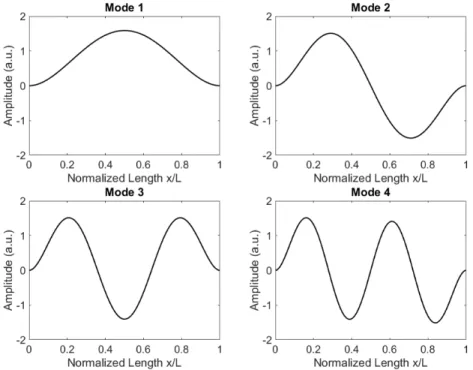
Figure 1.3: Mode shapes of a doubly clamped beam for n=1,2,3,4.
Z L 0
Un(x)Um(x)dx = L3δmn. (1.5)
Finally an arbitrary solution can be written as:
U (x, t) =
∞
X
n=1
an(t)Un(x). (1.6)
where an are dimensionless amplitudes. First four mode shapes of doubly
clamped beam is given on figure 1.3.
Table 1.1: Higher order solutions of a doubly clamped beam. Recreated using data from [21]. n=1 2 3 4 βnL 4.730 7.8532 10.9956 14.1372 ωn/ω1 1 2.756 5.404 8.933 A1n/L -1 -1 -0,9988 -1 A2n/L 0.9825 1.0008 0.9988 1.0000
1.3
Thesis Outline
Chapter 1 will serve as an introduction to nanoelectromechanical systems includ-ing a brief summary of the recent developments in the field, applications, and advantages of NEMS. A theoretical background on flexural vibrations of doubly clamped beams at nanoscale will be presented.
In Chapter 2, I will explain the microfabrication methods we used to build NEMS. Starting with a brief historical background on integrated circuit(IC) in-dustry, each fabrication step that was used during this MS study will be explained including the working principles of the procedures. Steps are roughly in the or-der of a fabrication process of a NEMS; starting from substrate cleaning proce-dures to final step of wirebonding of a finished device to a printed circuit board. Furthermore, process development steps for procedures such as dry etch recipe preparation, electron beam lithography dose testing will be discussed on a prac-tical level. Finally, detailed step by step fabrication process of a NEMS is given with each step visualized layer by layer in 3D. This chapter might serve as a guide for a graduate student who is just delving into the world micro/nanofabrication as well.
In Chapter 3, transducer mechanisms used for our NEMS will be explained. Electrothermal actuation is a tool to drive NEMS to higher order modes by Joule heating a bilayer structure. Advantages and drawback of this method will be discussed. In order to detect the nanomechanical motion of these sensors, piezoresistive down-mixing method was utilized. The geometric and material piezoresistivity will be explained. Drawbacks of DC biasing and the need for frequency down-mixing will be addressed. Finally, the electronic instrumentation used for the measurements will be discussed.
Chapter 4 presents two novel NEMS applications done during my MS studies. Intermodal Coupling, a new method to detect higher order modes of a nanome-chanical resonator, will be discussed. The second application is on Q factor control of nanomechanical systems based on a mesoscopic work done on linear
energy absorbing oscillators called energy sinks. Theories, experimental setups and results of these work will be explained.
The final chapter will serve a summary and outlook to this M.S. thesis. Possible improvements and future works will be discussed for the applications mentioned in this work and a very brief information on other applications that are still undergoing at the time this thesis was completed.
Chapter 2
Fabrication Methods for NEMS
Microfabrication is an engineering discipline that covers the methods for fabrica-tion for integrated circuits, microelectronics, MEMS, NEMS, and other related nanotechnology fields [22]. Dimensions of interest for microfabrication varies from atomically thin layers to hundreds of micrometers. With the integration of photolithography into microfabrication in 1960s [23], the IC industry grew rapidly alongside with microfabrication. While closely related to IC industry, very-large-scale integration (VLSI) deals with the design problem of fitting bil-lions of transistors on a semiconductor chip while microfabrication deals with how to fabricate those transistors. First transistor was invented in 1947 at Bell Labs and after only 70 years, 14 nm minimum feature sized chips with billions of transistors are in the market for consumer use.
Nanofabrication is often used as a term to define fabrication methods for de-vices with minimum feature sizes lower than 100 nm [24]. Nanofabrication can be divided in to two major branches: top-down and bottom-up fabrication. An analogy for top-down fabrication would be chiseling a marble block to remove unnecessary parts to obtain a statue while the bottom-up fabrication rely on self organization and precursors to add materials to create the devices. While both have different advantages and disadvantages this work mostly focuses on top-down fabrication methods.
All of the devices mentioned in this work was fabricated at Bilkent University affiliated facilities such as National Nanotechnology Research Center (UNAM) and Advanced Research Laboratories (ARL). This work will not include compar-ison between every available microfabrication method, instead it will focus solely on the procedures used. Besides, information such as the cost of individual steps used, as important as it is especially for the industry, is out of scope of this work as the first and foremost requirement to choose a method was the availability of that method at the facilities. Further information on microfabrication techniques can be found in the literature as there are many great sources available [25], [26], [27], [22].
2.1
Design
Similar to manufacturing, microfabrication requires detailed planning and design-ing. Layers are used to represent each physical stack of materials. It is important to understand and visualize these layers to comprehend the flow and logic of each step of microfabrication. By adding or subtracting materials from these layers a final functional device is created. In this work GDSII (Graphic Data system) file format, which is currently the defacto IC industry standard, was used. In order to organize and create these layers, GDSII editors can be used. There are many GDSII editors available in the market and a few that have been used in this work are Clewin, Layout Editor, and Elphy Plus GDSII editor.
During design process the operator should take into consideration the fabrica-tion limitafabrica-tions and feasibility before proposing a design. For example, fabricating very large contact pads (>200 µm) with electron beam lithography would take a lot of time and when there are 100 devices on a chip, it becomes unpractical. Instead, contact pad layer can be realized with photolithography and the de-vice layer can be aligned later using electron beam lithography. Another example would be minimum feature sizes and error tolerances. For example, electron beam lithography device at UNAM has an error of 50 nm for each alignment procedure due to manual alignment procedure. In this case feature sizes smaller than 50
Figure 2.1: A multi layered GDSII design. Each layer is represented by different color and texture. Often numbers and markers are added for easier identification.
nm on different layers could not be fabricated reliably.
2.1.1
Design Rationale
The goal was to design mechanical resonator that can reach higher order modes. The doubly clamped beam was chosen instead of other mechanical structures because of the selected integrated transducers (electrothermal actuation and piezoresistive detection) which were to be placed in separate ends of the res-onator to prevent any cross-talk between the transducers. Another incentive was that doubly clamped beams are established in the field and are used frequently for mass sensing applications [13, 14] and as a research group we have more expe-rience with doubly clamped beams. In order to prevent any impedance mismatch with 50 Ω detection equipment our integrated transducers were also needed to be 50 Ω. In order to achieve this we designed the Au electrodes to have 50±10 Ω.
silicon nitride which was commercially available and purchased from a supplier. First of all due to our transducers we needed an insulator device layer to prevent any shorts for the electronic circuit. A material with low thermal expansion coefficient was required compared to Au as the actuation mechanism depended on it [28]. Relatively low cost, good thermal resistance, and high Young’s modulus made silicon nitride our choice of device layer instead of other common device layers such as SOI, SiC, SiO2.
The high frequency responses of NEMS increase the detection speeds [10] and also has shown to increase the Q factor for bio-sensing applications [29]. Yet, with very high fundamental frequencies the higher order modes quickly get into microwave range and is not always easy to detect. In order to utilize these higher order modes and still attaining the high frequency response, we decided to keep our devices fundamental mode around 10 MHz. Since the device thickness was fixed from the supplier we determined the length of our initial devices at 10 µm which resulted in approximately 13 MHz fundamental frequency following the equation 1.3.
Our fabrication iterations showed that with 10 µm beams we can fit 4 modes under 100 MHz which will be useful for our mass sensing applications while at the same time allowing 13 MHz fundamental frequency for high speed measurements (figure 3.5).
2.2
Sample Preparation
Sample preparation is one of the most important steps of any fabrication process. There are many possible sources for contaminants which can lead for undesired results during fabrication such as airborne particles in the atmosphere, solvent stains, dust from the environment, skin flakes from the operators, etc. For ex-ample a strand of human hair, which is around 75-150 µm in diameter, left on a substrate before spin coating would render a photoresist layer useless. Moreover, there are many contaminants that are larger than the minimum feature size of
the devices that could seriously tamper with the fabrication. For example a 64-kB dynamic memory chip has a minimum feature size of 2.5 µm and could only tolerate 0.25 µm particles in the atmosphere [27].
To prevent all these sources from tainting the samples, fabrication must be done in specialized laboratories called cleanrooms which are enclosed areas where pressure, temperature, humidity and airborne particles are constantly controlled and regulated. Clean rooms are classified depending on the average particle size per cubic foot in the environment. The facilities of UNAM are 100 class clean rooms based on the U.S. federal standards. Furthermore, users should wear appropriate gear and follow gowning procedures to enter clean rooms. At all times, samples must be handled with utmost care, the device layers on top of the substrates should not be touched or scratched.
Even though clean rooms are absolutely necessary for microfabrication as a preventative measure for contamination they are not enough. Newly grown or commercially obtained wafers and samples that are being reused after certain procedures must go under a series of cleaning steps in order to get rid of any organic, ionic, or native oxide residues on the surface. For instance, when silicon wafers are not used for a certain amount of time; the surface atoms reacts with the oxygen in the atmosphere, creating a thin oxide layer. If an operator tries to deposit contact pads on top of such sample, assuming the sample is clean, those pads will not be electronically connected to silicon surface due to the insulating oxide layer in between.
The samples used in this work had gone through RCA wet clean procedure when first obtained. RCA clean was developed by Werner Kern while working at Radio Corporation of America in 1965 [30]. RCA clean has become the industry standard and used for new wafers out of the box and also before high tempera-ture treatments such as oxidation, diffusion and so on. It is a two-step cleaning procedure where RCA-1 strips organic residues and RCA-2 ionic contaminants of the substrate. RCA-1 is particularly useful to clean samples after a failed pho-tolithography step as it strips away all the organic photoresist residues. Steps and solvent ratios of the procedure could be modified and optional steps could be
added depending on the fabrication. Both RCA-1 and RCA-2 procedures leave a thin oxide layer on top of the surface; therefore, a third step of a quick HF dip is necessary to get rid of the oxide layer. If the samples are visibly contaminated, a piranha solution (a mixture of sulfuric acid and hydrogen peroxide) can be applied as preliminary cleaning. A step by step RCA clean procedure, based on [31], used in this work on newly acquired wafers are shown on appendix A.
If we consider RCA a hard clean for newly acquired wafers, there is also a soft cleaning procedure that involves sequential rinsing of the sample with acetone, isopropanol alcohol (IPA) and deionized (DI) water. This procedure should be applied after almost all steps of fabrication, excluding when there is an organic layer on the surface or there are suspended structures. Sample should be soaked in an acetone bath and then rinsed with flowing acetone. This step should be repeated using IPA. The sample must be rinsed with a DI water gun or flowing DI water afterwards. Finally, the sample must be dried with a nitrogen gun. If necessary a 1 minute 120◦C bake could be applied to get rid of humidity. The operator must be swift during these steps and should not allow any of the solvents to evaporate on the substrate as it could leave residues.
Commercially available wafers usually come in as 4 or 6 inch discs. While in IC industry even larger wafers are used during fabrication, for research and prototyping purposes smaller samples are desirable most of the time since they are easier to handle and during development many samples might get destroyed. In this work 10 mm x 10 mm square samples were used for both development stages and final devices; since the NEMS are very small, a single device, including contact pads, usually cover 500µm × 500µm space. The samples were diced out of 4 inch wafers. An automated diamond saw was used to ensure that each chip is at the same size. In order to protect the substrate from saw dust, the wafers were coated with a thick layer of photoresist before dicing. An acetone bath after, will strip away to resist make sure that the chips can be removed easily.
2.3
Lithography
Lithography refers to the pattern transfer method invented by Aloys Senefelder in 1796 as a cheap printing method and until 1950s was mostly used for artistic purposes [27]. With the addition of photomasking and chemical processing pho-tolithography was developed. Following this first commercial ICs were introduced in 1961. Pattern transfer methods used in this work are photolithography and electron beam lithography.
2.3.1
Photolithography
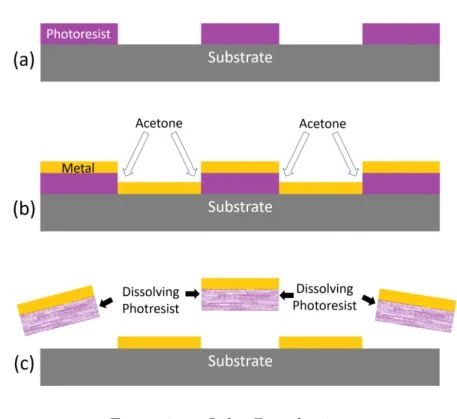
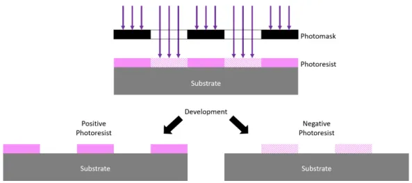
Photolithography is the foundation upon which the microelectronics and IC in-dustry is built upon. It is a method of pattern transfer from a photomask to a substrate by exposing organic photo-sensitive materials called photoresist to ultra violet (UV) light. Photoresists are photoactive organic polymers mixed with solvents and when exposed to UV light, undergo a chemical reaction which strengthens or loosens the bonds between their molecules depending on the resist type. If the exposure strengthens, cross-links, the bonds; it is a negative photore-sist whereas if the exposure loosens, due to chain scission, the bonds; it is called a positive photoresist (Figure 2.3). In this work, positive photoresists were used and for remaining part of this section each photoresist mentioned will be positive.
In order to transfer the pattern, the exposing UV light must masked by a tomask. For this work commercially available 5 by 5 inches soda lime glass pho-tomasks were used. One side of the glass is coated with 5300˚A AZ1500 photoresist on top of 1200˚A opaque chromium layer. The design, drawn in a GDSII editor, is then patterned to the mask using a mask writer which is a laser or electron beam lithograph. After the patterning, the photomask is developed in a solution and depending on the photoresist type, positive for this case, exposed or unexposed parts of the photoresist is dissolved (Figure 2.2). Now the exposed parts of the chromium layer can be wet etched by a commercially available chromium etchant while the remaining photoresist act as a etch mask. This process of mask making
Figure 2.2: GDSII design of contact pads (a) patterned onto a 5 inch soda lime photomask (b) by a mask writer.
is essentially a full fledged fabrication by itself.
2.3.1.1 Spin Coating
Spin coating is a method to coat a substrate with photoresist. Sample is spun at very high speeds (typically 1000 to 6000 rpm) to ensure that liquid photoresist spreads uniformly on the surface. There are other methods of photoresist coating such as spray coating, dip coating and so on.
After sample surface is prepared, it must be baked on a hot plate at 120◦C for one minute to ensure there is no moisture on the surface which can affect the adhesion of the photoresist. On some occasions certain photoresists do not adhere well to the substrate surface even after dehumidifying step. In such cases, as an optional step, the surface can be further primed by spin coating an adhesion promoter such as Hexamethyldisilazane (HMDS) before photoresist coating. The sample is placed on a spinner and fixed by a backside vacuum. Photoresist is poured on the sample with a plastic pipette. The sample is spun at desired rpm to achieve a certain resist thickness which depends on parameters such as molecular weight, solvent percentage, viscosity. While corresponding thickness can be calculated there are spin curves for each photoresist, available from their
respective manufacturer.
If the surface was not cleaned properly and there are solid particles that are at similar size or larger than the photoresist thickness they will cause streaks. Operator should make sure that during the pouring step no bubbles form on the resist. These imperfections would cause a nonuniform resist thickness which could influence the results of subsequent steps.
After the spin coating, the solvent part of the photoresist does not evaporate completely and could contain built in stresses [27]. In order to evaporate the solvent, the sample must be heat treated. This step, called the soft bake or pre-bake, can be done by baking the sample on a hot plate, typically 1 minute at 90 − 110◦C. The bake temperature and duration depends on the resist type, desired thickness and exposure parameters. The soft baked sample is now ready for exposure.
2.3.1.2 Exposure and Development
Exposure step involves exposing the photoresist layer to UV light while masked by a photomask as shown on figure 2.3. When required, a handheld UV flash light can be used; however, for almost all processes an exposure tool should be used. In UNAM there are mask aligners that can be used for exposure. These tools allow for alignment between different layers and controlled exposure of the samples. There are two main exposure methods for photolithography: shadow printing and projection printing [25]. Projection printing allows for exposure of numerous wafers at the same time allowing high throughput fabrication. In this study proximity printing method was deployed where the photomask is in close proximity to the substrate.
Molecular bonds at the exposed regions are loosened and will be now dissolved by a step called development. Each photoresist have corresponding developer which dissolves the photoresist. For positive photoresist, the exposed parts be-come extremely soluble compared to unexposed parts. Development parameters
Figure 2.3: Exposure Process and effect of UV radiation on positive resist (a) and negative resist (b).
are determined according to the resist type, resist thickness, and exposure levels. Developer can be diluted with water to decrease the development rate.
Development process involves dipping the exposed sample into a diluted de-veloper for timed duration. After the duration is over, the sample is rinsed with DI water immediately to stop any remaining developer to further react with re-sist. At this step optical microscopy should be used determine the success of development. If the exposed photoresist did not dissolve completely (underdevel-opment), a subsequent development can be applied. On the other hand, if the development was too much: process duration could be decreased, developer can be further diluted or the exposure dosage can be lowered.
After development, sample is usually hard-baked to ensure even better adhesion between photoresist and sample surface by evaporating any remaining solvent. If material will be deposited on top of the photoresist, typically 30-60 seconds bake on a 110◦C hard plate can be applied. If the resist is going to be used directly as an etch mask, even longer bakes at higher temperatures must be applied to further strengthen the resist. Either way this is the last step of a typical photolithography process.
2.3.2
Electron Beam Photolithography
Electron-beam lithography (EBL) is a high resolution direct writing method. Direct writing refers to the fact that there is no need for a mask in order to transfer a pattern. Instead of UV light, focused electron beams (e-beam) are used for exposure. Thus EBL is not limited by the diffraction of light and can be used to pattern sub 100 nm features. Electron-beam sensitive resists (e-beam resist) are used as a substitute to photoresist. Other than these differences EBL process steps are similar to photolithography.
There are two types of EBL setups. First type is essentially a modified scan-ning electron microscope (SEM) where the SEM is converted with an appropriate pattern generator hardware and software to an EBL. The other types are stan-dalone EBL with automatic stitching and marker detection features. The EBL used in this MS study was one of the former, a FEI SEM that is converted to an EBL by a RAITH pattern generator module which manipulates the magnetic coils and beam blanker that turn on and of the beam to direct the beam to different points on the sample.
Even though state-of-the-art photolithography techniques, i.e. extreme UV lithography, are able to reach similar features sizes as EBL; they need very ex-pensive devices and are not cost effective without fabricating thousands of devices with each batch. For research purposes and prototyping, where high throughput is not necessary, EBL offers a cost effective replacement for writing linewidths smaller than 1 µm. Even though EBL is mostly used for mask writing in the industry, it has become an indispensable tool for research oriented fabrications.
2.3.2.1 E-beam Resist
Poly(methyl metacrylate), PMMA for short, is a commonly used e-beam resist. Similar to photoresists, e-beam resists are polymers mixed with certain solvents to modulate viscosity and resist thickness. For instance, PMMA A4 495k is an e-beam resist frequently used in this work. In this case, 495K refers to the fact that
this PMMA has a molecular weight of 495 kDa. A4 means, PMMA is dissolved in anisole and solid contents in this resist are 4% by weight. Anisole can also dissolve plastics; thus a glass pipette should be used when pouring this PMMA on substrates.
E-beam resists, like photoresist, can be spin coated on the substrate. Spin curves are available from manufacturers. Due to the feature sizes involved are smaller than photolithography e-beam resist layers tend to be much thinner com-pared to photoresist. As a result, e-beam resists are not very suitable as hard etch masks. While lift-off is relatively easier for EBL due to inherent undercutting, a bilayer resist can be applied to achieve even more pronounced lift-off geometries. A higher molecular weight resist is coated on top of a lower molecular weight resist which requires a lower electron dosage for dissolution, resulting in a better undercut after development [32]. A commonly used bilayer e-beam resist recipe (Table 2.1) used in this work results in 300 nm PMMA thickness.
Due to electron penetration, the minimum feature size of EBL is affected by the resist thickness. A rule of thumb for 30 kV electron acceleration is: the resist thickness should not be more than 3 times the desired minimum feature size. For instance for 100 nm features, the resist must not be thicker than 300 nm.
Table 2.1: PMMA bilayer spin coating recipe for 300 nm thick film. 1- 10 minute bake on hotplate at 180◦C
2- PMMA 495K A4 at 2000 RPM for 40 seconds (215 nm resist thickness) 3- 5 minute bake on hotplate at 180◦C
4- PMMA 950K A2 at 3000 RPM for 40 seconds (80 nm resist thickness) 5- 10 minute bake on hotplate at 180◦C
2.3.2.2 Exposure and Development
Instead of UV light, EBL uses an e-beam to expose the resist. Generated electrons are charged by electrostatic fields up to 100-200 keV then the beam is focused and narrowed by a system of magnetic lenses and apertures [32]. The current of the e-beam can be measured by a Faraday cage on the stage that is connected to
Figure 2.4: Dose factors for the same design. (a) has no proximity correction while (b) is proximity corrected.
a multi-meter. Since EBL is not limited by the diffraction of light, it possible to achieve smaller minimum feature sizes down to few tens of nanometers. However, the feature sizes are limited by electrons scattering into the resist and back-scattering from the substrate [25].
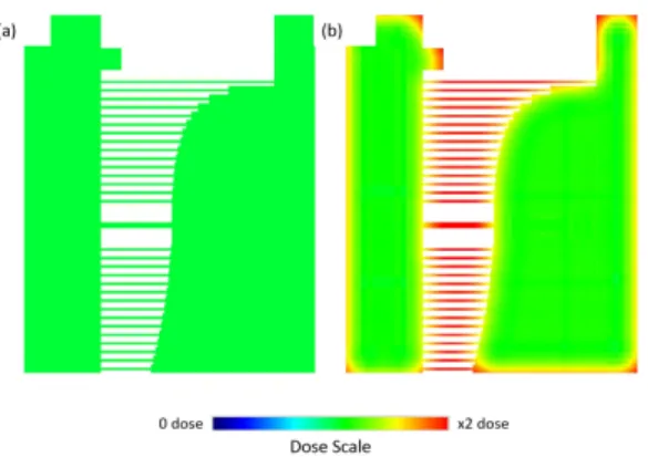
The lateral scattering also causes an issue called proximity effect. Since the exposed areas are larger than the spot size, due to scattering, the neighboring patterns affect each other. Thus, correction is required to calculate optimum ex-posure dosage at local patterns. These corrections are called proximity correction which depend on the resist type, resist thickness, substrate type, and e-beam volt-age and current. These corrections requires cumbersome calculations; fortunately, there are pre-calculated corrections available for commonly used substrates and resists. In this work corrections available from RAITH EBL software library were used.
On figure 2.4a, dose factor is same for each part of the design. In this case, the smaller beam like structures in the center would not receive enough dosage while the large clamp areas do not require as much dose since the exposed are is large. Furthermore, centers of those beam would be thinner than the base of the beams affecting the geometry. Figure 2.4b is the corrected version where smaller features and edges receive higher dose and central parts of larger geometries receive less.
electron beam current. For the EBL setup used in this work, the beam speed should not exceed 10 mm/s since magnetic coils do not work properly at higher beam speeds.
Development step is very similar to photolithography. Exposed sample is dipped in developer for a certain amount of time to dissolve exposed parts of the resist. A common developer used for PMMA is Methyl isobutyl ketone (MIBK). Typical PMMA development process can be seen on table 2.2.
Table 2.2: PMMA development procedure. 1- 1 minute dip in MIBK:IPA(1:3) solution 2- 5 seconds MIBK:IPA(1:1) dip.
3- 30 seconds IPA dip to stop the reaction. 4- N2 drying.
2.3.2.3 Dose Test
EBL is a very complex fabrication step with numerous parameters from resist thickness to electron beam current that severely affect the process outcome. Thus, before starting a new design a dose test must be done. Operator must ensure that each test sample has same thickness of resist and has gone thorough identical procedures. Design must be patterned on to the test sample at separate locations, with sufficient distance and varying exposure doses. After development, the spec-imen must be characterized with an SEM to analyze and decide on the optimal dosage. Operator must be swift and use the beam blanker during the imaging process as SEM imaging is essentially electron bombardment of the sample and further exposure occurs. Although it is time consuming and not necessary at all, an optional metallization followed by lift-off can be applied to the dose test samples. This way, the patterns will not be affected by the SEM imaging and the characterization could actually give more information.
A typical example of dose test is shown on figure 2.5. A design is patterned with increasing doses, developed and imaged with SEM. If the dose was not sufficient, PMMA will not develop properly (figure 2.5a). On the other hand if
Figure 2.5: Dose test characterization by SEM. 10 identical design with varying dose factors (d) were patterned. Closer examination shows: overexposure (a), optimal dose (b), and underexposure (c). Scale bars are 4 µm for top row images and 50 µm for (d).
the exposure is too much the electrons will scatter farther and the unintended parts of the resist will develop (figure 2.5c). Using small enough increments it is possible to locate an optimal dose (figure 2.5b) with closest dimension to the design. Development duration can be also altered to control the features sizes. After an acceptable dose is determined, the operator can use the settings to pattern the actual samples.
2.3.2.4 Alignment
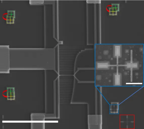
Alignment is a process that allows for the EBL software to recognize a position on the physical plane of the stage and align those markers to the design plane. It works by moving to alignment markers that are either patterned before or are a part of the bare substrate. E-beam is controlled with magnetic coils; consequently, the writing area, writefield, is limited. If the design is larger than the maximum writefield possible, it cannot be patterned with one step. Furthermore, most of the work done in this study involved patterning of more than one layer which requires the sample to be taken in out of the chamber more than once. In such cases an alignment procedure must be done to stitch larger designs or different layers. While automatic marker detection was possible within the RAITH software, SEM column limited it to manual marker detection. Therefore alignment procedures were the most tedious and time consuming part of the fabrication.
Markers should be easily identifiable and distinguishable, especially when there is more than one alignment step. Further, the markers should be large enough to accommodate stage errors. Figure 2.6 shows the initial locations of marker scans in green. Even though the scans are not precisely on top of the markers, small part of the markers are still visible. If not, the operator could not align at all. This scan procedure exposes the resist and these locations gets deposited. Therefore the marker locations should be far enough from the device features.
Since the mechanical stage of the EBL had an error of 10 µm for 100 µm lateral step, there was a need for alignment after each time the stage moved. For electrothermally actuated NEMS fabricated in this work, the error tolerance was
Figure 2.6: SEM image of a NEMS device that had gone through 2 alignment procedures. Green cross-hairs marks the initial point of the marker scans and yellow cross-hairs the aligned position. Red box shows one of the markers of the alignments step for the previous layer. Inset shows a closed up view of an alignment marker. Scale bars are 40 µm and 4 µm.
50 nm. A comprehensive checklist to operate Raith Elphy Plus EBL software during alignment procedure can be found on appendix B.
2.4
Evaporation
Evaporation is a subset of physical vapor deposition, a commonly used thin film deposition method that can separated into two groups: physical vapor deposi-tion (PVD) and chemical vapor deposideposi-tion (CVD). “CVD essentially involves the
process of dissociation of molecules of the gaseous reactants, which subsequently react chemically to form various structures when activated by heat, light, or plasma discharge” [24]. In PVD, on the other hand, the target material is heated up and goes under a physical state change. While it is mostly used for metal deposition some semiconductors and oxides can be deposited as well. (Si, Ge, SiO2, TiO2, etc.) Some examples of PVD methods are as following: sputtering,
molecular beam epitaxy, ion plating and, so on. However this work will focus on evaporation.
Evaporation is done in a vacuum chamber so that the atoms in vapor can directly move toward the substrate and strike the surface to form a thin layer [26]. If there is not a sufficient vacuum, the atoms in the vapor would collide with atoms present in the chamber and might not reach the substrate surface. Even if it does reach the surface, the particles in the chamber atmosphere could stick to the vapor; which would contaminate the deposited layer. Therefore, the pressure must be at the levels at which the mean free path of the molecules are larger than the distance between the target material and the substrate surface. Evaporation should be performed at pressures around 10−6 Torr [22]. In order to achieve these pressure levels, a rough pump accompanied by a turbo molecular pump, or an oil diffusion pump must be used.
The thickness of deposited films can be monitored by thin-film thickness mon-itors. Usually a quartz crystal micro-balance is used as the sensor. Rate monitor is placed to a close proximity to the substrate. When the material is being de-posited on the substrate, because of the close proximity, the crystal will be also covered with the deposited materials. By tracking the resonance frequency of the crystal, which will decrease with the deposition of new material due to added weight, it is possible to measure the film thickness. Since there would be an inevitable difference between the amount of material that strikes the substrate and the crystal a calibration must be made. These calibrations, although can be calculated very precisely, usually are done empirically. Typical parameters of a thickness monitor are: Tooling factor, material acoustic impedance and ma-terial density. After certain amount of usage the crystal must be changed as its sensitivity will decrease. The operator should make sure to track the crystal
Figure 2.7: Step coverage of evaporation and sputtering. Adapted from [33].
lifetime.
During the deposition, substrate temperature will increase since target mate-rial is heated to its melting point. Moreover, the deposited film will be very hot. If the vacuum is breached immediately, the room temperature atmosphere could cool down the thin layer very rapidly which could cause the film to buckle under these quick changes in thermal stress. In order to prevent this, the substrate should be allowed to rest for 15-20 minutes under vacuum before braking it.
Because of this “ballistic” [26] deposition, where the atoms in the vapor strike directly to the substrate surface, there is an issue of step coverage with evapora-tion methods (Figure 2.7). In order to overcome this limitaevapora-tion substrate rotaevapora-tion and heating could be applied. Or another thin film deposition method sputtering could be used when step coverage is required for the fabrication process. How-ever, step coverage can be detrimental for lift-off purposes, which will be covered in the next section. Thus, this limitation in step coverage was actually desired for this study.
2.4.1
Thermal Evaporation
Thermal Evaporation is an additive pattern transfer method that utilizes DC electric current to heat the target material to its melting point to deposit the
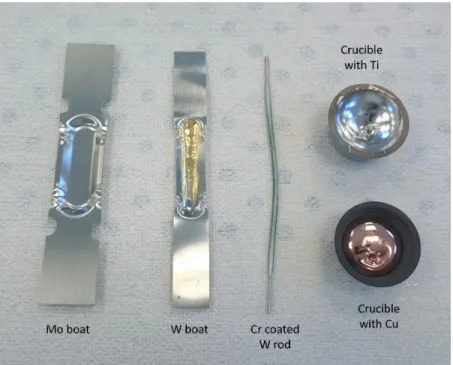
Figure 2.8: Few example of boats and crucibles used for evaporation.
material onto the substrate. Figure 2.9 shows inside a thermal evaporator cham-ber. In thermal evaporation, target material is put in to a metallic boat. As high current passes through the boat (figure 2.8), typically around 100 A, both the boat and target material heats up. While there is always an equilibrium of vapor pressure above the material [26]; in order to achieve reasonable deposition rates the target material is heated up until molten state. Obviously, the melting point of the material should be lower than the boat itself or the boat will melt and the evaporation process will fail. With thermal evaporator, it is possible to deposit materials with melting point up to 1800◦C. For materials with lower melting points, such as Au and Ag, molybdenum boats are used. For higher melting points, i.e. Cr, tungsten boats are more suitable as molybdenum boats would fail. There are also rods coated with evaporation material available. In this work chromium coated tungsten rods were used for chromium deposition (Figure 2.8).
During thermal evaporation it is important not to change the current passing through the boat rapidly. First of all, sudden changes in temperature can break the boat and stop the whole procedure. Moreover, it can affect the thin film uniformity if the deposition rate keeps changing. Additionally, initial deposition
Figure 2.9: Inside of a thermal evaporator chamber. This particular thermal evaporator has three target holders which can be used subsequently for layer by layer deposition or simultaneously for alloy deposition.
rate must be very slow to ensure adhesion to substrate. The first few nanometers would acts a seed layer and rate could be increased after. It is good practice to start with 0.1˚A/s for 2 nm and then increase the rate. Usually passing 1 ˚A/s is not advised for thermal evaporator. However, e-beam evaporation is not affected by this 1 ˚A/s limit as crucibles are much more sturdy than boats.
2.4.2
Electron Beam Evaporation
For materials with higher melting points, an e-beam evaporator can be utilized (Figure 2.10). Instead of a DC electric current, a magnetically steered [26] elec-tron beam, typically around 10 kV , is used to heat up the target material. Cru-cibles are used for e-beam evaporation which are placed in water cooled hearts to accommodate the high temperatures. Another advantage of e-beam evaporator is the higher deposition rate due to the higher temperatures can be reached with electron beam. In this work, e-beam evaporator was used for copper etch mask deposition. While thermal evaporation could also be used to deposit copper, the deposition rates are much slower than the e-beam evaporation.
2.5
Lift-off
After lithography process, a thin layer can deposited on to the substrate to fill the patterns. To complete the pattern transfer, a method known as lift-off must be applied. The sample is soaked in an acetone bath for 6 or more hours, depending on the feature sizes, to strip away the resist and the deposited material on top of it. For NEMS device layers in this work, overnight lift-off was used to ensure proper lift-off. At this time the lid of the bath should be sealed to ensure that acetone will not evaporate completely. Failure to prevent acetone evaporation could cause in a failed lift-off; moreover, solvents should never be allowed to evaporate on substrate surface normally.
Figure 2.10: Inside of an e-beam evaporator chamber. Target material is put in a crucible that goes to the crucible holder which sits on top of a water cooled hearth. The mirror is used to visually track the electron beam which should be directed on to the crucible. This particular e-beam evaporator can hold four crucibles at the same time but does not allow for simultaneous deposition.
Figure 2.11: Lift-off mechanism.
after metallization (Figure 2.11 b). Acetone starts to dissolve organic photoresist where it can reach it. Dissolving photoresist strips away with the metal layer on top of it (Figure 2.11c). After the process is over; the sample should be put in a sonic bath for a short duration, typically a minute, to strip away any remaining resist. However, this sonic bath should not be overdone or the deposited thin layer could be stripped away as well. If done correctly, the desired pattern is now transferred on to the sample.
For a successful lift-off, the thumb of rule used for this work was the 1 to 3 ratio. The resist thickness should be at least 3 times thicker than the deposited material in order to ensure a successful lift-off, especially for submicron structures. Otherwise, acetone might not seep through the crevices between deposited layers and resist. This a very important rule to follow especially for submicron features as acetone has to physically reach the underlying resist. This is the reason why for a lift-off process the step coverage is not really desired as it would prevent acetone to reach underlying resist. The 1 to 3 ratio rule is more flexible with larger feature sizes. Figure 2.12 shows two examples where 3 to 1 ratio was not
Figure 2.12: Examples of unsuccessful lift-off procedures. Both scales bars are 5 µm.
followed and the lift-off was unsuccessful as acetone could not seep into small features.
2.6
Etching
Etching is a subtractive fabrication method where materials which are not pro-tected by an etch mask, are stripped away either chemically, physically or with a mixture of both. After the lithography step, a sample can go through etching process directly or another step of thin layer deposition or oxide growth might be applied before etching. There are to two types of etching: wet and dry.
2.6.1
Wet Etching
In wet etching, the sample is dipped into a liquid solution, called etchant, that would react with sample surface. In some cases vapor of the etchant can be also applied. Wet etching mechanism involves three steps: reactants in the etching solution reaches to the surface, chemically reacts with substrate surface and the products from the reaction are removed by diffusion [25]. The removal rate from the surface is deterministic for the etch rate. This diffusion can be controlled by the temperature of the etchant. Physical removal of byproducts also affect the etch rate, for example stirring the solution.
Figure 2.13: Stiction of a silicon beam after HF based oxide wet etch. Scale bar is 5 µm.
One of the biggest disadvantage of wet etching is the stiction caused by the liquid meniscus left under suspended structures during drying (Figure 2.13). This liquid pocket pulls the structure to the substrate surface with capillary forces as it evaporates. After the evaporation, suspended structure might stick to the surface due to the strength of Van der Waals forces at small scale. This is especially critical for cantilevers and very long and thin features. To overcome this issue a critical point dryer can be utilized.
Wet etching is highly selective due to its chemical nature. Moreover, etch isotropy is affected by the crystal structure of the material. However, for shallow etches, under 1 µm, it is hard to time the etch correctly since etch rates are relatively higher compared to dry etch. In this work, wet etching was used to strip away metallic dry etch masks.
2.6.2
Dry Etching
Dry etching is a subtractive method where solid surfaces etched by a gaseous species. Dry refers to the fact that in no step of etching, the sample comes into contact with wet chemicals. This eliminates any stiction problem that may
occur. Moreover, especially with submicron features, wet etchants sometimes cannot seep into every crevice whereas in dry etching gaseous molecules can move more freely. Dry etch can be physical (ion bombardment, sputtering), chemical (radical) or both pyhsical and chemical (reactive ion etching (RIE)) [27]. In a purely physical etch, (i.e. ion milling) inert species, such as Ar, are directed to the substrate surface with high energy, dislocating the atoms. In radical (chemical) dry etch, the ionized reactants form molecules with the substrate atoms and these volatile compounds are then pumped away. RIE, by combining both reactive (chemical) and nonreactive (physical) gasses together utilizes the selectivity of the chemicals and anisotropy of the high energy ions.
Dry etching uses gas or vapor plasma created by an electric field to etch the substrate. This plasma can be created with DC, AC (50 kHz and up), RF (13.56-27 Mhz), or microwave fields (300 MHz and up). When an electric field with sufficient magnitude is applied to the gas, free electrons oscillate and collide with gas molecules ionizing them [25] creating a quasineutral plasma which has equal number of positive and negative charges. This high energy reactive plasma then reacts or collides with the substrate surface.
In this work, plasma was created at RF frequency by an inductively coupled plasma (ICP) device. In the upper part of the chamber a coil operating at 13.56 MHz (communications standard) drives the plasma inductively and creates a low pressure, low energy, and high density plasma (figure 2.14) while the 13.56 MHz platen at the bottom of the chamber modulates the ion bombardment energy [27]. The substrate then gets bombarded with ions, reacts with the plasma which etches the sample.
Selectivity is an important parameter of etching as it is a measure of etch rate ratios between a target material being etched and the masking material. The mask could be either a deposited thin film, a layer of grown oxide, or a photoresist. In order to etch targeted locations and mask the others, there must be enough selectivity between the materials. For example 100:1 selectivity between a target material and mask would mean that 100 unit of the material is etched by the time 1 unit of mask material is etched. Higher selectivity is desired for an etch but in
Figure 2.14: Schematic of an ICP chamber. Adapted from [34].
some circumstances a thicker mask can circumvent this need. After many tests, e-beam evaporator deposited Cu etch mask was used in this work. It is highly resistant to fluorine based etch and can be removed easily with a commercially available aluminum etchant.
In this study, RIE of silicon and silicon nitride was utilized. Etch mechanism depends on many parameters. First of all the selected etchant species should react with substrate. For silicon and silicon nitride, fluorine based etches are quite common resulting in volatile SiF4 by products. The chemistry is as followed
[32]:
Si + 4F → SiF4
Si3N4+ 12F → 3SiF4+ 2N2
(2.1)
Free fluorine can be generated by fluorinated gasses. CF4 and SF6 ionization
e−+ CF4 → CF2+ 2F
e−+ SF6 → SF5+ F
(2.2)
In this work, the goal was to suspend silicon nitride doubly clamped beams on sacrificial silicon layer. In order to achieve this, silicon nitride must be etched first. To achieve a prismatic beam geometry with perpendicular side walls the etch must be anisotropic and the undercut should be minimized. Increasing the ion bombardment energy by biasing is one of the most influential way to achieve better anisotropy. Additionally, using inert molecules, such as Ar, will increase the anisotropy. However this method result in heavy ion bombardment of the substrate and requires a very strong and thick mask. Yet, the feature sizes of our devices did not allow mask thickness more than 100 nm. Moreover, the substrate surface could be damaged by these high energy ions.
Another option is to inhibit the reaction by coating the substrate with a poly-mer. This is called wall passivation. By adding fluorocarbons (i.e. CHF3, C4F8)
to the gas mixture, polymerization on substrate surface can be achieved which will block the reactions. Although polymerization occurs both on vertical walls and horizontal surfaces, the high energy ions in the plasma will quickly etch the horizontal surfaces; yet, the vertical walls will not be affected by these ions as the electric field does not direct the ions on the walls. Wall passivation is an important aspect of RIE and was very critical for the development of deep RIE which is used to etch hundreds of microns deep into silicon substrates. Thus, a recipe based on CF4 as free fluorine source with additional wall passivation was
used. In order to etch silicon isotropically, SF6 was used. CHF3 was also added
to protect the silicon nitride device layer. Etch recipe and ICP parameters for these two process is given on table 2.3.
2.6.2.1 Recipe development
Recipe development was an important and time consuming part of this study. While selectivity of many materials and corresponding etch mask could be found

![Figure 2.7: Step coverage of evaporation and sputtering. Adapted from [33].](https://thumb-eu.123doks.com/thumbv2/9libnet/5666834.113362/41.918.187.773.181.401/figure-step-coverage-evaporation-sputtering-adapted.webp)