CHEMICAL VAPOR DEPOSITION
OF
BORON NITRIDE NANOTUBES
A THESIS
SUBMITTED TO THE DEPARTMENT OF CHEMISTRY
AND THE GRADUATE SCHOOL OF ENGINEERING AND SCIENCE OF BILKENT UNIVERSITY
IN PARTIAL FULFILLMENT OF THE REQUIREMENTS FOR THE DEGREE OF
MASTER OF SCIENCE
By
NİYAZİ OKAN ÇİFTCİ JUNE, 2013
ii
I certify that I have read this thesis and that in my opinion it is fully adequate, in scope and in quality, as a thesis for the degree of Master of Science.
………. Assist. Prof. Dr. Erman Bengü (Advisor)
I certify that I have read this thesis and that in my opinion it is fully adequate, in scope and in quality, as a thesis for the degree of Master of Science.
………. Assoc. Prof. Dr. Dönüş Tuncel
I certify that I have read this thesis and that in my opinion it is fully adequate, in scope and in quality, as a thesis for the degree of Master of Science.
………. Prof. Dr. Oğuz Gülseren
Approved for the Graduate School of Engineering and Science: ……….
Prof. Dr. Levent Onural Director of the Graduate School
iii
ABSTRACT
CHEMICAL VAPOR DEPOSITION OF BORON NITRIDE NANOTUBES
Niyazi Okan Çiftci
M.Sci. in Department of Chemistry Supervisor: Assist. Prof. Dr. Erman Bengü
June, 2013
Since ancient times materials that are available and used by people constitute indispensable constituent parts of world history. The historical ages are named after the materials which paved an irrevocable way to this stream and revolutionize the progress of history by changing the rhythm of anthropological breakthrough irreversibly.
People have used these materials either directly borrowing from nature or by transforming those that are given. As we approach to modern society two methods namely a top-down method using transmission of experiences of before generations conventionally and bottom-up method by application of modern science and technology to understand subtleties of materials and engineering them for the specific goals.
Boron nitride nanotubes are one class of these materials having superior properties to the conventional ones. High strength, electrically insulator property, controllable wide band gap and high oxidation resistance as compared to carbon nanotubes put them to the first ranks for the design of the future devices for our modern society. Hence a simple and inexpensive way of production of this kind of materials is utmost importance.
For this in this thesis an inexpensive and a very practical way of BNNTs production is elucidated. The reactants boron (B), iron (III) oxide (Fe2O3) and magnesium oxide
iv
(MgO) are used as solid precursors. A CVD furnace reaching up till 1200 oC with a special design of added concentric quartz tubes equipped with NH3 and Argon gas
served as reaction chamber.
v
ÖZET
BOR NİTRİD NANOTÜPLERİN
KİMYASAL BUHARLARIN ÇÖKTÜRÜLMESİ YÖNTEMİ İLE ÜRETİLMESİ Niyazi Okan Çiftci
Kimya Bölümü Yüksek Lisans Danışman: Assist. Prof. Dr. Erman Bengü
Haziran, 2013
Antik dönemlerden günümüze değin insanoğlunun kullandığı malzemeler dünya tarihinin vazgeçilmez bir parçası olmuştur. Tarihin akışını ve insanoğlunun yeryüzündeki öyküsünü geri döndürülümez bir biçimde dönüştüren ve ona her zamankinden farklı bir sıçrama yetisi kazandıran malzemeler bu dönemleri adlandırmıştır.
İnsanoğlu bu malzemeleri ya olanları dolaysızca ya da elde bulunanları dönüştürerek kullanmıştır. Günümüze geldiğimizde ise bu erek için iki tür yöntemin belirdiğini görüyoruz; geçmiş nesillerin deneyimlerinin geleneksel bir biçimde aktarıldığı yukarıdan-aşağıya ve çağdaş bilim ve teknolojinin öncülüğünde malzemenin özellik ve inceliklerinin anlaşıldığı böylelikle belirli bir amaç için işlevselleştirildiği alttan-üste yöntemi.
Bor nitrid nanotüpler geleneksel malzemeler ile karşılaştırıldıklarında özellikleri ile öne çıkan malzemelerdir. Yüksek mukavemet, elektriksel yalıtkanlık, kontrol edilebilir bir bant aralığı ve de yükseltgenmeye karşı yüksek dirençleri onları karbon nanotüpler ile karşılaştırdığımızda çağdaş toplumun gelecekte gereksinim duyacağı ürünlerin üretilmesinde en ön sıralara yükseltmektedir. Bu malzemelerin üretiminin yaygınlaştırılması için pahalı olmayan ve de ulaşılabilir bir yöntemin geliştrilmesi büyük önem taşımakta.
Bu doğrultuda bu çalışmada ucuz ve ulaşılır bir yöntemle BNNT üretimi açıklanmıştır. Bor, demir (III) oksit (Fe2O3) ve magnesium oksit katı tepkime
katılıcılarına ek olarak azot kaynağı olarak da amonyak gazı NH3 kullanılmıştır.
Tepkimenin gerçekleşeceği yüksek sıcaklık derecelerine yükselen fırının içi özel bir biçimde içiçe geçmiş kuartz tüplerle düzenlenmiş ve amonyak gazı ile içeride bulunan tepkime kayıkçığına yerleştirilmiş katı katılımcılar tepkimeye sokulmuştur.
vi
Tepkime sırasında oluşan aratürlerin buharları silicon alttaşları üzerine eklenmiş değişik türden katalizör katmanları aracılığı ile çökelerek bor nitrid nanotüpleri oluşturdukları Raman spektroskopisi, Taramalı Elektron Mikroskopu (SEM), X-ışını fotoelektron Spektroskopisi (XPS), Enerji Saçılımlı X-ışını Analizi (EDX), X-ışını kırınım spektroskopisi aracılığı ile kanıtlanmıştır. Bunun yanında su damlacıklarının BNNT kaplı yüzeyler üzerindeki tutunma davranışı dokunma açısı ölçümü cihazı ile bulunmuştur.
vii
ACKNOWLEDGMENTS
I hereby acknowledge the support of the people whose presence invisible to the reader in the thesis. They are overshadowed under my name and I cordially want them to appear in the following lines.
First and foremost I thank my advisor Assist. Prof. Dr. Erman Bengü for giving me an original and challenging work to do which awakened my scientific interest to see the fate of a fog condense into a crystal future. Hence I thank him for companying me and making the walk amusing with his friendly conversation.
I thank also Assist. Prof. Dr. Göknur Cambaz Büke for contributing to my studies with orientation and coadvising.
I am grateful to Cemal Albayrak for various talks about Varlık through experience and form as we call them language and philosophy. Beside every concept there is a wreck of experience as in science lots of experiments behind theory.
In addition to this I must thank Hüseyin Alagöz for his help in various types of instrumentation.
Not only we talked too much but we had pretty much fun especially through “Düşuyayteş”. My friends who understood and appreciated its value Gözde Barım, Batuhan Kav, Elif Mercan, Pelin Altay and M. Burak Şenol, Benjamin Reimold I am thankful to these friends of mine from Bilkent University.
From METU my friends Melike Berksöz and Maksat Babayev for their precious friendships and their understandings.
For Tuvan throat singers and Shamans for their transmission of ancient wisdom of our ancestors and paving way for hope, love and light in the midst of mother nature. For my family; my mother Songül Canbulat, brothers Ozan, Orhan and my sister Oya Bilge Çiftçi and for its nextcoming generations I dedicate this thesis.
viii
TABLE OF CONTENTS
CHAPTER 1 ... 1 1. Introduction ... 1 CHAPTER 2 ... 5 Background ... 5 2.1 Nanotubes ... 52.2 Boron Nitride Nanotubes ... 8
2.3 Synthesis techniques for BNNT ... 11
2.4. Properties and Applications of BNNTs ... 13
CHAPTER 3 ... 15
3. Experimental Results ... 15
3.1 Growth of BNNTs ... 15
3.1.1 Catalyst Preparation ... 15
3.1.2 Chemical Vapor Deposition ... 17
3.1.2.1. Experimental setup: ... 17
3.2 Characterization Techniques ... 21
3.2.1 Scanning Electron Microscopy: ... 21
3.2.2. Energy Dispersive X-ray Analysis ... 21
3.2.3. X-Ray Photoelectron Spectroscopy ... 22
3.2.4. Raman Spectroscopy ... 22
3.2.4. X-Ray Diffraction: ... 23
3.2.5. Contact Angle Measurement ... 23
CHAPTER 4 ... 24
4. 1. EXPERIMENTAL RESULTS and EVALUATION ... 24
Contact angle measurement: ... 48
CHAPTER 5 ... 52
Conclusion ... 52
ix
LIST OF FIGURES
Figure 1. Plot showing the increase in transistor counts in CPUs by the year they
were launched. Courtesy of Wikipedia (6). ... 2
Figure 3. Different allotropes of carbon ... 7
Figure 4. Crystal structure of hexagonal boron nitride ... 8
Figure 5. Single walled BNNTs ... 9
Figure 6. The numbers of papers as emerged in scientific journals regarding BNNTs. ... 10
Figure 7. The method of catalyst surface production ... 16
Figure 9. The heating regime of the furnace ... 18
Figure 10. Chemical vapor deposition system for the production of BNNTs ... 19
Figure 11. Chemical vapor deposition system for the production of BNNTS (real picture) ... 19
Figure 12. The classification of experiments ... 24
Figure 14. Products without using MgO (only B+Fe2O3) ... 25
Figure 15. Raman spectrum of products synthesized with B+MgO+Fe2O3 in 4:1:1 molar ratio respectively. ... 25
Figure 16. SEM images of products synthesized with B+MgO+Fe2O3 ... 26
Figure 17. Raman spectra of bare steel and BN products synthesized on it showing a peak at 1367 cm-1 ... 26
Figure 18. SEM images at various scales... 27
Figure 19. EDX mapping results for a) Oxygen, b) Iron, c) Nitrogen, d) overall ... 27
Figure 20. Raman spectra showing a peak at 1367 cm-1 ... 28
Figure 21. XRD spectra for different planes of h-BN. ... 28
Figure 22. XPS results give a B/N ratio of 30.9 /42.45 = 0.72 almost equal to unity. ... 29
Figure 23. a) Oxygen, b) Nitrogen c) Silicon d) Iron... 29
Figure 24. a) SEM image b) overall mapping result c) elemental spectra ... 30
Figure 25. SEM image at various magnifications 1200 C, 4:1:1, 400 sccm NH3 flow ... 30
Figure 26. Raman spectrum ... 31
Figure 27. SEM image at various magnifications 1200 oC, 4:1:1, 300 sccm NH3. ... 31
Figure 28. a) SEM image b) Nitrogen c) Oxygen d) Chromium e) Iron f) Silicon g) overall mapping result h) elemental EDX spectrum ... 32
Figure 29. Raman spectrum ... 33
Figure 30. XRD spectrum showing peaks at various planes of h-BN. ... 33
Figure 31. SEM images at various magnifications 1100 411 200 sccm NH3 ... 34
Figure 32. Raman spectrum ... 34
Figure 33. XRD spectrum ... 35
x
Figure 35. Raman spectrum ... 36
Figure 36. SEM images at various magnifications revealing less BNNTs production on stainless steel 4:1:1 molar ratio, 1100 oC, 400 sccm, 400 mg reactants. ... 36
Figure 37. Raman spectrum ... 37
Figure 38. SEM images at various magnifications for 1000 oC, 4:1:1, 300 sccm NH3 flow. ... 37
Figure 39. Raman spectrum ... 38
Figure 40. SEM images at various magnifications MgO 400 sccm 411 1200 C ... 38
Figure 41. Raman spectrum ... 39
Figure 42. SEM images at various scales for the run 1200, 4:1:1 300 sccm NH3. .... 39
Figure 43. Raman spectrum ... 40
Figure 44. SEM images at various scales MgO 1100 4:1:1 400 sccm NH3... 40
Figure 45. Raman spectrum ... 41
Figure 46. SEM images at various magnifications for 1100 oC, 300 sccm NH3, 4:1:1 molar ratio ... 42
Figure 47. Raman spectrum ... 42
Figure 48. SEM images of BNNTs on Ni catalysts at 1200 oC, 8:1:1, 300 sccm NH3. ... 43
Figure 49. Raman spectrum ... 43
Figure 50. SEM image showing no BNNTs formation Ni 1200oC, 8:1:1 molar ratio, 200 sccm NH3 mass flow. ... 44
Figure 51. Raman spectrum showing a strong peak around 1360 cm-1 and various other weak peaks. ... 44
Figure 52. SEM images showing very rare covering of the substrates coated with Ni Ni 1200 oC, 4:1:1 molar ratio, 200 sccm NH3 mass flow... 45
Figure 53. Raman spectrum ... 45
Figure 54. SEM images at various magnifications of the Ni coated substrates 1200 oC 411 300 sccm NH3 ... 46
Figure 55. Raman spectrum shows a sharp peak at 1367 cm-1 ... 46
Figure 56. SEM images at various magnifications showing BNNTs on iron coated substrates Fe 4:1:1 1200 oC, 200 sccm NH3. ... 47
Figure 57. a) Iron b) Nitrogen c) Silicon d) Oxygen e) SEM images f) overall mapping result ... 47
Figure 58. Contact angle values of ddH2O on BNNT coated surfaces with respect to time. ... 48
Figure 59. a) overall mapping b) nitrogen c) EDX spectrum of elements ... 49
Figure 60. SEM images of micro-tubes filled with nanotubes ... 50
Figure 61. SEM images of so-called nano-mushrooms at various magnifications. ... 50
xi
LIST OF ABBREVIATIONS
BNNTs boron nitride nanotubes h-BN hexagonal boron nitride
c-BN cubic boron nitride
CNTs carbon nanotubes C60 Buckminsterfullerene
CVD chemical vapor deposition MFC mass flow controller MFCC MFC controller
sccm standard cubic centimeters per minute RS Raman Spectroscopy
SEM Scanning Electron Microscopy EDX Energy Dispersive X-ray Analysis XRD X-ray Diffraction Spectroscopy XPS X-ray Photoelectron Spectroscopy
1
CHAPTER 1
1. Introduction
In 2003, during a lecture series Richard E. Smalley, co-recipient of the 1996 Nobel Prize for Chemistry, declared a list of Top Ten Problems Facing Humanity over the next 50 years(1). Furthermore, an institute established in his name, The Smalley Institute, within Rice University has reduced these ten problems in to five Grand Challenges – energy, water, environment, disease, education(1). In conclusion, the Smalley Institute cites these problems in order to advocate the urgency and necessity for the development of new and innovative technologies, processes and especially materials for overcoming these challenges. For the last several decades, the growing population of the earth and its consumption of natural resources including energy and clean water have begun straining the delicate balance in the environment and even the world peace. In order to increase the efficiency of energy consumption and improve clean water storage, usage and recovery, scientists have been doing research on new materials which may enable exploration of new paths for remedying the Grand Challenges.
Recently, nanotechnology has emerged as an interdisciplinary platform for physicists, chemists and researchers from other related fields which has demonstrated a significant potential for the discovery and synthesis of unique materials potentially capable of providing solutions to upcoming challenges to the human existence on earth as cited above, e.g. fullerenes (2), nanotubes (3), and graphene (4). Discovery or synthesis of new materials may also have reverberating and unprecedented effects in other fields such as information technologies which can be considered as an enabler technology for the advancements needed. For instance, increasing the computational power and efficiency of computers can significantly shorten the time required for solving problems in clean energy and clean water shortage which indirectly will ease many of the issues faced with regards to environmental pollution experienced by many countries. Furthermore, diseases such as cancer, genetic disorders and others could well benefit from drastically increased speeds of
2
computers for the formulation of new molecules and treatments. In the case of education, cheap and fast access to information through internet and also processing of information can help eradicate the educational disparity between the kids in the impoverished regions of the world and those that live in developed countries. Therefore, such advancement can easily level the playing field for the upcoming new generations which will certainly have an effect in unifying the nations of the earth in a more peaceful manner.
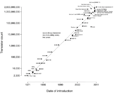
Figure 1. Plot showing the increase in transistor counts in CPUs by the year they
were launched. Courtesy of Wikipedia (6).
It is very well-known within the current scheme that the number of transistors per unit area on a central processing unit (CPU) of a computer directly influences computational performance. Hence, Gordon Moore, co-founder and Chairman Emeritus of Intel Corporation, has published an article in 1965 (5) where he stated that the number of components (transistors) in integrated circuits had roughly doubled between 1958, inception of integrated circuits, until 1965 and he also indicated that it was well within reason to expect for this trend would continue "for at least ten years" (5). This assertion has become to be known as the “Moore’s Law” which fueled the race for cramming more and more transistors per unit area on a silicon wafer, as shown in Figure 1. In Table 1, transistor density data for some of the microprocessors included in Figure 1 are provided, which also shows that the
3
process node that is used. Unfortunately, the down side of increasing the number transistors on silicon is that one has to also decrease the critical dimension of the transistors which is known as the gate length of a metal oxide semiconducting field effect transistor (MOSFET). Hence, there is a physical limit as to how small the gate length could be pushed, due to quantum tunneling of electrons in a semiconductor in this case silicon. Zhirnov et al in 2003 (6) has come to the conclusion that in order to scale classical MOSFETs beyond the 22 nm node (corresponding to 9 nm gate length) new and novel materials and perhaps new designs are needed. In fact, at least two of the assertions by Zhirnov et al has been materialized; 1)- the use of high-K dielectric materials as the gate oxide and, 2)- novel new transistor designs, such as the use of finFET type transistor (7) technology which is commercialized by Intel Corporation in 2012 (8). Even with these advancements, in order to continue doubling the computational power of computers other advancements are needed as the limit in silicon is in sight.
During the meantime, new types of materials emerged, these are essentially 1-D and 2-D materials, where one or more dimensions of the materials are limited to nanometer scales. Two simple examples are carbon nanotubes (9) and graphene (4). Naturally, there have been new transistor designs making use of carbon nanotubes (10–16) and graphene (17–29). The premise of application in the field of semiconductors and also in other fields had stirred enormous scientific interest and activity on the 1-D and 2-D carbon allotropes. However, there are a multitude of problems for the application of these new structures as an alternative to silicon even dismissing those related to mass production. One of the major problems is that both CNTs and graphene have low resistance to oxidation when exposed to relatively low temperatures (150 °C). For example, the lifetimes of CNT based FETs are cited to be couple of days under ambient conditions (30). Therefore, for certain real world applications nanotubes and/or single layer sheets made up off materials with oxidation resistance could be significantly useful. Hence, there are similar 1-D and 2-D structures made up off more heat and oxidation resilient materials such as boron nitride (BN). Unfortunately, there has been much less activity around nanotubes and single layer sheets of BN when compared their carbon counterparts. This is mainly due to 1-D and 2-D structures of BN being relatively harder to synthesize.
4
While, there will be more information provided regarding BN nanotubes (BNNTs), the main motivation behind the work provided in this thesis is the mass production of BNNTs on a suitable substrate material through chemical vapor deposition which would then enable and/or ease their usage in diverse fields such as electronics and even in medicine. In the following sections, a short background on the discovery and properties of nanotubes is provided and also a literature survey on BNNTs is given. In chapter 2, a detailed summary of the experimental procedures including the design and building of the CVD system used in the works and also the characterization techniques utilized for the examination of the products of the CVD experiments will be given. In chapter 3, the results of the experiments will be discussed comparatively with the literature. There will be a conclusion section presented in chapter 4 summarizing the work presented in this thesis.
5
CHAPTER 2
Background
2.1. Nanotubes
Nanotube is a branch of compounds which have a very small diameter as compared to their lengths. Hence they can be conceptualized as one-dimensional materials. In nature several atoms, molecules and compounds have the capability to form tubular structures. The rule of thumb for a compound to be able to form nanotubular morphologies is first its ability to form stable layered structures. The most popular layered structures to be known are graphite, hexagonal boron nitride, transition metal dichalcogenides. By simply wrapping these layered materials into seamless cylinders give rise to tubular structures. That is why carbon nanotubes (9), boron nitride nanotubes(31) BxCyNz nanotubes (32), tungsten (33) and molybdenum (34) disulfide nanotubes appeared in the literature. From these nanotubes CNTs and BNNTs are focused in the following lines.
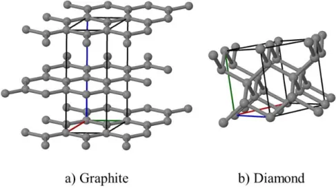
Carbon because of its unique electronic structure can assume a range of crystal structures. These allotropes of carbon range from the hardest materials known, diamond, to the soft and lubricious graphite; crystal structures for graphite and diamond are given in Figure 2 a and b respectively.
6
Figure 2. The crystalline structures of a) graphite b) diamond
Due to the characteristic of the sp3 bonding hybridization for the case of diamond and sp2 hybridization for graphite, markedly differing electrical and physical properties for these structures are observed. For example, while the bulk modulus of graphite is around 30 GPa(35) in the direction perpendicular to the hexagonal carbon planes, the bulk modulus for diamond is approximately 430 GPa (36). However, it has to be noted that in plane bulk modulus of graphite is reported to be around 545 GPa due to the shorter C-C bond length (1.43 Å) than that is reported for diamond ( ~ 1.54 Å) (37). Electronic properties of graphite are also drastically different than for diamond such that graphite is a metallic conductor while diamond is a semiconductor which can be doped both p- and n-type. There has been reports of devices are made from diamond films (38), however it has to be mentioned that n-type doping is significantly challenging (39).
Due to the weak van der Waals type of bonding between the carbon layers in graphite, it is very easy for these layers to slip on each other making graphite a lubricious material. Whereas, in the stacking of diamond the carbon atoms are ‘bent’ out-of-the plane of the (111) crystal planes forming the so-called the corrugated structure with the angle between C-C-C chain is about 109.5 (120° for graphite). The strong bonding between the C atoms of the subsequent (111) planes constitutes the essence of the extreme hardness of diamond.
7
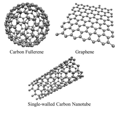
During the last 2 or more decades, existence of various other allotropes of carbon has been demonstrated which are not readily encountered in the nature; these are namely carbon nanotubes, graphene and various different fullerenes (2–4, 9). See Figure 3 for the atomic models of these phases.
Figure 3. different allotropes of carbon
The first successful synthesis of single-walled CNTs has been reported by Iijima (9). However, soon it was understood that there were earlier reports of studies depicting CNTs through low resolution transmission electron microscopy dating back to 1952 (40, 41) far earlier than the first popularization in 1991. Single-walled CNTs (SWCNTs) may exhibit varying electronic properties stemming from the change in rolling directions; chirality. They may be either semiconducting or metallic conductors.
In the years following the landmark reports of Iijima (3, 9) regarding CNTs, there have been reports commenting on the existence of BN nanotubes (BNNTs) through experiment (42) and theory (43). BNNTs are modeled as rolled single sheets of
8
hexagonal (graphitic) boron nitride forming tubular structures. Unlike CNTs, computational studies indicated that BNNTs are all insulators with a large band gap 5.5 eV (44) . This makes the electrical properties of BNNTs very predictable and hence garnering an advantage over CNTs as mentioned earlier electronic properties of CNNTs are uncontrollable which may restrict their technological applications. In the following section, a literature review of the BNNTs will be provided.
2.2. Boron Nitride Nanotubes
3A group element boron and 5A group element nitrogen form compounds that are isoelectronic with that of 4A group element carbon. Then a spectra of various morphologies ranging from layered to tubular for the compounds isoelectronic with carbon is intelligible. Some of these compounds have been known for a long time. Hexagonal boron nitride composed of sp2 hybridized boron and nitrogen atoms forming a network extended in two dimensions; a structural analogue of graphite and cubic BN composed of sp3 hybridized boron and nitrogen atoms forming a network in three dimensional space as do carbon atoms in diamond structure. In figure 4 the crystal structure of h-BN are shown.
9
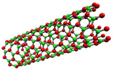
Therefore after some time elapsed from CNTs’ popularization first theoretical papers appeared in the literature predicting the possibility of existence of boron nitride nanotube(44). BNNTs are modeled as composing of rolled hexagonal (graphitic) boron nitride to form tubular structures. BNNTs are just like hexagonal boron nitride has in plane strong sp2 bonds and between the planes weak Van der Waals forces. In this paper it was also proposed that it is energetically more favorable to form BNNTs by rolling h-BN rather than rolling graphene into CNTs(43). In the theoretical papers on BNNTs it was shown that as the BNNT structure relaxes back and the boron and nitrogen atoms do not stay on the same plane. Rather B atoms penetrate inside the hollow side of the tube approaching to the tube axis and N atoms move away from the tube axis hence forming two concentric planes(45). Also in this paper it is shown that by simply looking at the tip ends of the tubes synthesized it is possible to estimate their chiralities; flat ends are preferred in zig-zag tubes, chiral tubes are ended with some amorphous BN compounds and lastly armchair tubes prefer conical ends.
Figure 5. Single walled BNNTs
Single walled CNTs exhibit different properties stemming from their way of rolling and chirality. SWCNTs may be either semiconductors or conductors whereas BNNTs are semiconductors with a large band gap of 5.5 eV (44). This is due to the fact that although CNTs are covalent and composed of only one element, BNNTs are composed two elements differing in electronegativity constituting a covalent
10
compound with slightly ionic characteristics. This ionicity of the B-N bond widens the energy difference between valence and conduction bands. The value of band gap depending on the curvature of the nanotubes increases and the value finalizes in that of h-BN 5.5 eV which can be conceptualized as lowest curvature. This property of electrical predictability of BNNTs is advantageous over CNTs because electronic properties of CNNTs are uncontrollable and thus are their technological applications restricted. Also the band gap of BNNTs can be tuned or changed permanently with several physical methods.
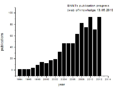
Figure 6 shows the number of peer-reviewed papers published each year regarding BNNTs between 1994 and 2012. This plot indicates that the numbers of studies on BNNTs are increasing every year. However, it still less than those found for CNTs, and as indicated earlier it is believed that the main reason for BNNTs lagging the interest that is enjoyed by CNTs is that synthesis of BNNTs are harder and requires higher temperatures.
11
2.3. Synthesis techniques for BNNT
In this part of the thesis, a brief summary on the synthesis techniques used for BNNTs in the literature will be given.
As mentioned earlier, the first successful synthesis of BNNTs followed a report suggesting their existence through theoretical study (44). On the other hand, the first successful method of production of BNNTs were achieved by arc-discharge synthesis (31). In this study, hexagonal boron nitride is used as a starting material. Since h-BN is an insulator it could not be used as an electrode, instead it is filled into a hollow tungsten electrode which was used as anode and as a cathode a copper electrode was used. The vacuum chamber is filled with ammonia and a constant pressure is maintained during discharge. Multi-walled BNNTs were observed exceeding 200 nm in length and capped at their ends with tungsten particles in the soot collected inside the vacuum chamber. This first report was followed then by studies indicating the identification of single and double walled BNNTs in a similar arc-deposition experiment using an HfB2 electrode as the anode and graphite
electrode as the cathode under an inert N2 atmosphere (46). However these BNNTs
were found to be closed-capped with planar layers not contaminated with catalytic particles. These planar closed ends of the tubes are perpendicular to the tube axis. Moreover, similar reports of BNNT formation through arc-deposition using Ta-BN electrodes (47) under an inert N2 atmosphere were made as well. In this case, both
closed end tubes and those with metal particles were observed. In another study utilizing arc-discharge method, (48) boron-rich electrodes including nickel and cobalt were used again under a N2 atmosphere environment. This method produced a
large amount of double walled BNNTs.
The first successful laser ablation based BNNT production is achieved in 1996(49). A boron target is heated with the help of a laser beam under an N2 atmosphere at an
elevated pressure and temperatures reaching 5000K. By using this method, presence of multi-walled BNNTs was reported. In another study (50), laser irradiation heating of h-BN under pressure values of 10 G Pa in a diamond anvil cell up to temperatures 5000 K was conducted which resulted in the formation of multi-walled BNNTs, also. Following these, excimer laser ablation of h-BN at 1200°Cwere conducted (51). The products from this study were found to be single, double and triple walled BNNTs.
12
The tips of the nanotubes were found to be either terminated with polygonal caps. Bulk production of BNNTs are also reported through laser heating of a BN target in a low pressure N2 atmosphere (52). Characterization of reaction byproducts included
double walled BNNTs and closed BN-cages.
Other than arc-discharge and laser including techniques, chemical vapor deposition (CVD) method is also successfully used for the production of BNNTs. Using in situ generated borazine, B3N3H6, and nickel boride catalyst particles at a temperature of
1100°C multi-walled BNNTs are produced (53). In another CVD approach starting from B4N3O2H as a precursor, multi-walled BNNTs are produced(54). It is suggested
that silicon, aluminum and calcium incorporated in nano-clusters made of boronoxynitride are responsible for the BNNTs growth. The same authors also synthesized predominantly cylindrical BNNTs (55).
FeO, MgO and B are also employed in other variants of CVD techniques (56) where an induction furnace with a BN boat and ammonia, as a nitrogen source, were utilized. Pure BNNTs are produced in large amounts by this method. Moreover, similarly starting from very simple precursors such as B, MgO, and Fe2O3 synthesis
of BNNTs are accomplished at relatively low temperatures such as 1200 °C (57, 58). Heating MgO and B in an rf induction furnace with the supplement of NH3 gas has
also been reported as a productive approach for synthesizing BNNTs (59).
Substitution reactions using CNTs as templates is another route used for the production of BNNTs. In this method CNTs are used as disposable templates. Boron and nitrogen atoms from gaseous precursors substitute carbon atoms in CNTs through the massive amount of vacancies generated on graphitic networks of CNTs upon heat treatment(60). In another method, single walled BNNTs and boron and nitrogen doped CNTs are produced following a similar route (61). The synthesis conditions employed involved heat treatment of SWCNTs in the presence of B2O3
and nitrogen flow between 1523 and 1623K. Depending on the temperature of the process BNNTs were formed at temperatures above 1530°C and, boron and nitrogen doped CNTs at temperatures around 1250-1350°C values were reported. Complementary to this, the temperature dependence of the product conversion from BxNyCz are described elsewhere by using thermo-gravimetric analysis (62). It is
13
to CO and CO2 formation between 550-675°C. In the next step, the mass did not
change between 675-800°C interval due to resistance of BNNTs toward oxidation. Above 800°C BNNTs dissociate giving off boron oxide and N2 as by-products,
which also proves that BNNTs are significantly more resilient to high temperatures. Bengu et al. synthesized single walled BN nanostructures with atomic deposition technique and characterized the products in situ without giving rise to any contamination (63). In this technique, an electron cyclotron resonance microwave generated N2 plasma source and an electron beam evaporator for B have been used to
synthesize BNNTs on tungsten and copper substrates. Ball-milling followed by heat treatment is also another way reported for the production of BNNTs(64). Boron powders are ball-milled in ammonia gas for 150 hours. BNNTs and other crystalline boron nanoparticles were observed. It is reported that this method results in the formation of bamboo-like BNNTs in which iron particles of iron balls serve as catalyst for the growth. In another method instead of boron directly hexagonal boron nitride is ball-milled (65) and bamboo-like morphologies of BNNTs were observed. Also steel balls were used for the milling of elemental amorphous boron in an NH3
atmosphere and heat treated at 1100 C in a quartz furnace(66). By this method BNNTs longer than 1.0 mm are obtained.
Plasma-jet method (67) is another method being successfully utilized for the synthesis of BNNTs. As a starting material, sintered BC4N sintered bodies were used
and as plasma gases nitrogen and hydrogen gas mixture were employed. However products formed contained a spectrum of nanotubes multi-walled BNNTs, CNTs and their mixtures.
2.4. Properties and Applications of BNNTs
As compared to their CNT counterparts BNNTs has a high oxidation resistance as mentioned earlier. Oxidation of CNTs start at 500°C however for BNNTs this is as high as 800°C (62, 68). The thermal stability of BNNTs and them being a wide band gap semiconductor regardless of the number of walls and chirality (43) allow BNNTs to be a feasible material for various applications. Among these, one of the most important is that they can be used to manufacture nanometer sized electronic devices operating at elevated temperatures for integrated circuits. Other unique properties of
14
BNNTs namely high thermal conductivity (69) and superior Young modulus of approximately 1.2 TPa (70) allow them to be an additive to various materials for reinforcement and, heat dissipation for future devices and technologies. Even small amounts of BNNTs as an additive to some polymeric materials namely to polystyrene and poly-methyl methacrylate are observed to enhance their thermal conductivity with factors of approximately 20 and 21, respectively(71). The electrically insulating nature of BNNTs also can be used for the covering of metallic CNTs preventing current leakage(72, 73).
Hydrogen storage is another possible application of BNNTs(74). It is predicted that due to ionic nature of the hetero-atomic B-N bonds in BNNTs it can serve as a better hydrogen storage material as compared to homo-atomic C-C bond in CNTs (75). Moreover depending on the decrease of curvature of the tubes due to change in the diameter of the BNNTs amount of hydrogen absorption can be manipulated. Also specific surface area is found to be directly related to the amount of the hydrogen gas absorbed(76).
BNNTs are partially ionic materials with a wide 5.5 eV gap band (43). Upon introducing of dopants this band gap can be narrowed down. For instance upon carbon doping of BNNTs band gap reduces and turns into semiconductor (77). Piezoelectric behavior for BNNTs has also been reported. In order to investigate this behavior, an in situ bending of an individual BNNT is done using a special sample holder (with STM capability) in a TEM. It was reported that the stress applied induced an electrical transport(78). This piezoelectricity property of BNNTs can be used for the targeted drug delivery systems which utilizes the property of BNNTs of converting sound waves into electrical signals(79).
Finally, it was reported that BNNTs have water repellent super-hydrophobic characteristics(80). This property of BNNTs makes it a good candidate for biomedical applications (81) as a substitute for cytotoxic CNTs(82).
15
CHAPTER 3
3. Experimental Results
3.1 Growth of BNNTs
For the synthesis of BNNTs in this work, a unique CVD system has been designed and built. With this CVD system, more than 120 experiments have been conducted during this work. Throughout these experiments, there have been updates and modifications to the CVD system due to knowledge gathered during these experiments. Hence the depictions presented in this chapter will be regarding the final setup.
In this work, BNNTs were deposited on a surface which will be regarded as the substrate from now on in this manuscript. For some of the experiments, a special treatment of the substrate surface has been conducted for the growth of BNNTs, this includes the application of a “catalyst” layer on top of the substrate surface. The application of the catalyst layer is limited to the Si (100) type surfaces. On the other hand, stainless steel substrates did not receive any catalyst layer application. In the following sections, first the preparation and application details of the catalyst layers are explained. Following this, details of the CVD system used and the experimental parameters are provided. Finally, brief descriptions of the characterization techniques utilized for the examination of the BNNTs are explained.
3.1.1 Catalyst Preparation
In this study, for the production of BNNTs a simple procedure is followed for the application of the catalyst layers on top of the Si (100) substrates. The procedure starts with the cleaving of Si (100) substrates to an approximate size of 10 mm by 10 mm square chips. These Si(100) surfaces are oxidized for about half an hour in a furnace open to ambient air that was heated to 900 °C. From the earlier works, it is known that this oxidation process creates approximately a 30Å thick oxide layer.
16
After this oxidation process, 5x10⁻⁵ mole of Al(NO3)3.9H2O (Aluminum nitrate, 98
%, Sigma-Aldrich) is dissolved in a 10 ml of ethanol (absolute for analysis Emsure), hence preparing a 5x10⁻³ molar aluminum nitrate solution. 40 μ ml of this solution is then applied to the surface of the oxidized Si(100) substrate with the help of a micropipette. After drying, Si (100) substrate is then heated at 200°C for half an hour. This induces the formation of an Al2O3 (aluminum oxide) layer on top the
oxidized Si(100) surface. The aim of introducing Al2O3 layer is due to the fact that it
can serve as an inhibitor and diffusion barrier layer for the next catalyst layers. Similar to the Al2O3 layer preparation, 5x10⁻⁵ mole of Ni(NO3)2.6H2O (nickel nitrate,
crystalline, Sigma-Aldrich), 5x10⁻⁵ mole of Fe(NO3)2.6H2O (iron (III) nitrate, 98%,
Sigma-Aldrich) and 5x10⁻⁵ mole of MgO (magnesium oxide, light extra pure, Merck) are separately dissolved in a 10 ml of ethanol (absolute for analysis, Emsure), hence preparing a 5x10⁻³ molar nickel nitrate, 5x10⁻³ molar iron (III) nitrate solutions and 5x10⁻³ molar MgO solutions, respectively. Then, several milliliters of these nickel, iron nitrate and MgO solutions are applied individually on the previously prepared Al-O surfaces using clean micropipettes. Similar to Al-O layer, after drying these layers are also subjected to 200°C for creating Ni-O and Fe-O layers on top of the inhibitor Al-O layer. Another catalyst, MgO (%YY, Sigma-Aldrich), is prepared by grinding powdered MgO using a pestle and mortar in ethanol. Furthermore, Fe-O, and Ni-O layers are further activated/reduced for some of the experiments in a separate tube furnace under H2 gas flow. Figure 7 depicts the sequence of the
application and preparation of Si(100) surfaces for BNNT synthesis prior to the placement of the substrates into the CVD furnace.
17
Figure 8. The amounts of the required catalyzers
In this study we also investigated the catalytic effect of bare stainless steel substrates on the production of BNNTs. Stainless steel substrates are used directly without introducing any extra processing that is application of Al-O inhibitor or catalyst (Fe-O, Ni-O or MgO) layers. Another ingredient in the CVD system is the alumina crucible where the Si(100) and stainless steel substrates are placed on. Also, inside the alumina crucible a powdered mixture of several reactants are placed; these are elemental boron (98%, Good Fellow Cambridge Limited), Fe2O3 (%99,
Sigma-Aldrich), and MgO (high extra pure, Merck). These reactants are used for producing volatile boron oxide compounds.
3.1.2 Chemical Vapor Deposition 3.1.2.1. Experimental setup:
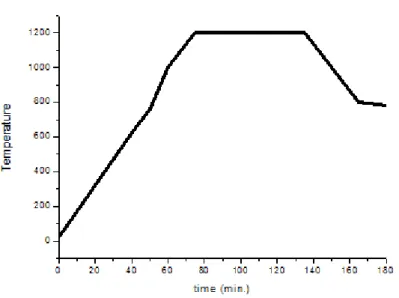
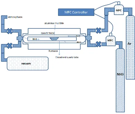
For the chemical vapor deposition production of boron nitride nanotubes a special tube furnace is designed and built. This system is capable of reaching temperatures above 1200°C. The heating profile used for the experiments are provided at Figure 9. Also, in Figure 10 a schematic description of the system is given. The CVD system is built around a quartz tube open at both sides. This quartz tube can work at 1200 °C without any interference to the reaction conditions. This quartz tube is 110 cm long and 6 cm in diameter. On both sides of the quartz tube vacuum tight stainless steel nipples are adapted. One side is used to ensure the gas connection for ammonia (4.5 purity, Linde) and argon gas (99.998%, Linde) delivery. The other side is used for attaching a roughing pump for pumping down the system before experiments. There are also two valves attached to each nipple for regulating the vacuum level inside the system. In order to maintain and control the gas composition in the system two mass flow controllers (MFC, MKS) used, one for ammonia (1479A02913C51) and the other is for argon gas. A special MFC for ammonia is used due to the corrosive
18
nature of this gas. The required amounts of gases for the reactions are monitored using an MFC controller (MANTIS). As indicated earlier, for the evacuation of the system a mechanical vacuum pump is used which is connected to one end of a “T” connector. The other end of the “T” connector a valve is attached which is isolating the system from the atmosphere.
An extra quartz tube resistant to high temperatures is placed inside the long quartz tube. It is 60 cm in length and 2 cm in diameter. One end of this smaller quartz tube open and the other is open as shown in Figure 10. The alumina crucible with the reactants and the substrates for BNNT growth are placed in the middle of this closed end quartz tube. In this crucible, the necessary reactants for the BNNTs production are placed.
At first a quartz crucible was used but it was found that the choice for quartz boat was not proper because reactants easily diffused into quartz at elevated temperatures. Hence, the crucible made of alumina was proven to be more robust. Inside the crucible elemental boron, MgO, and Fe2O3 in powder are mixed and is placed as
shown in Figure 8. Depending on the experimental run the molar ratios of the reactants are adjusted from 2:1:1, 4:1:1 to 8:1:1 respectively to investigate the effect
19
of the reactants on the production of BNNTs. This alumina reaction boat put into the closed end quartz tube is pushed to the very center of the furnace with a long stick before the closure of the furnace.
Figure 11. Chemical vapor deposition system for the production of BNNTS (real picture) Figure 10. Chemical vapor deposition system for the production of BNNTs
20
Once the system is closed and pumped down using the vacuum pump, the furnace is turned on. After approximately 40 minutes, the furnace reaches 625°C. At this point, Ar flow is allowed at a flow rate of 100 sccm in to the system. Approximately within 15 minutes of turning on the Ar flow, the furnace reaches 1000 °C. At this point, mechanical pump is closed and Ar flow is stopped. Then, immediately NH3 flow is
turned on 200 sccm depending on the experimental parameters decided upon beforehand. Once NH3 flow stabilizes within 40-60 seconds, the valve isolating the
system from the atmosphere is opened allowing the unreacted NH3 and reaction
byproducts to be swept into the atmosphere. After an hour at 1200 oC, the furnace starts the cooling period as shown in Figure 9 going back to 1000 oC. At this point, NH3 flow is stopped and Ar flow is started to purge the system and to stop the
reaction. Once the furnace cools down, one of the nipples is detached from the quartz tube and the crucible with the substrates is recovered for the upcoming characterization sequences.
21
3.2 Characterization Techniques
3.2.1 Scanning Electron Microscopy:
Scanning electron microscopy (SEM) is used for structures that cannot be seen with classical optical microscopy. For this a focused beam of electrons are used since the wavelength of electrons are smaller than that of the visible light so subtleties of morphologies of the specimens are made clear. Upon impingement of electrons to the specimen surface some part of their energy is transmitted to the specimen and secondary electrons are liberated from the surfaces of objects under investigation with SEM. These secondary electrons give information regarding the topography of the surface. Since these electrons are low in energy (20-500 eV) there is no other way of their being ejected from other regions except specimen. Qualitative data regarding elemental composition can be collected through exploitation of back scattered electrons which are produced upon elastic scattering by specimen atoms depending on their charges hence atomic number rather than atomic masses.
Scanning Electron Microscopy (Carl Zeiss Evo 40) equipped with an energy-dispersive X-ray (EDX) spectrometer is used for imaging and elemental determination in this study. Different voltage values ranging from 20 kV, 10 kV, 5 kV depending on the usage of energy dispersive X-ray analysis (EDS or EDX) and charging properties of surfaces coated.
3.2.2. Energy Dispersive X-ray Analysis
Electron bombarding the specimens in and SEM can also help eject electrons from the core levels of atoms comprising the specimen under analysis. Upon ejection of electrons from their base levels upper level electrons collapse into holes they left behind. This energy difference between levels is transmitted as x-rays. Energy and intensity of these x-rays are specific to the elements. Usually SEM and EDX are combined together for elemental analysis.
22
3.2.3. X-Ray Photoelectron Spectroscopy
Every part of electromagnetic spectrum is used for different kinds of spectral information about compositions of specimens. For surface analysis X-ray photoelectron spectroscopy (XPS) is employed. The surface is irradiated with x-rays whose energy is known. The energy of the X-rays is dissipated by knocking off the core electrons from the surface atoms. Kinetic energies of the free electrons are measured and subtracted from the incident energy of the X-rays (usually Al Kα). Because the binding energies of elements are specific to the elements, elemental and compositional analysis can be done. However, because of the escape depth of these electrons are very shallow, the analysis depth for this method is 1 to 10 nm.
The XPS characterizations of samples are performed in an ultra-high vacuum at a vacuum value of ~10-10 Torr. In this study, an XPS system composed of an XR50M X-ray Source, a Focus 500 monochromator and a Phoibos 100 type of energy analyzer made by Specs GmbH. The source of photoelectrons is Al Kα primary radiation with a monochromator. To eliminate charging effects, a flood gun is used with 30 µA current for all spectrum. For XPS analysis conducted in this work, the pass energy is set to 25 eV with an energy step width of 0.05 meV and a dwell time of 0.1 ms.
3.2.4. Raman Spectroscopy
This method relies on the interaction of a monochromatic light from a laser source with the molecular vibrations of the molecules. The resulting effect is an energy shift in the light which used for the estimation of vibrational modes in the system. There are three types of scattering in Raman Spectroscopy (RS); Rayleigh, Stokes Raman, Anti-Stokes Raman scattering. Rayleigh scattering is an elastic type of scattering giving no valuable information. When the light from the monochromatic source hits the object to be investigated, it excites the molecules from ground vibrational state to a virtual vibrational state. The relaxation from this level settles the molecule to another vibrational level giving off energy. The energy difference between this final state and the starting level causes a shift of energy of the monochromatic light. If the
23
final vibrational state of the molecule is lower in energy this is called Stokes Raman shift otherwise it is anti-Stokes shift.
For the Raman spectroscopy analysis, a LabRAM HR model micro-Raman equipment (Horiba Ltd., Kyoto, Japan) is used. For calibration before collecting data the spectrum is adjusted to zero wavenumber. The objective lens is selected as 50 times magnification. This data is averaged 10 times and the intensity is multiplied by 10 also.
3.2.4. X-Ray Diffraction:
X-ray diffraction is generally used for the estimation of the crystal structure of phases and even phase compositions. Upon interaction of X-rays with surfaces of crystals X-rays are diffracted at various angles. These angels are related to the wavelength of the x-rays and interplanar distances of the crystal structures, and the expression relating these two to each is
(1)
where, θ : angle between incident and reflected x-rays d : interplanar distance between the crystal planes λ : wavelength of the X-rays; commonly Cu Kα
The XRD patterns of the stainless steel samples were recorded on a Rigaku Miniflex diffractometer using source operating at 30kV/15mA. The distance between the atomic layers of the materials are investigated with a wavelength of 1.5405 Å source of a high power Cu Kα.
3.2.5. Contact Angle Measurement
The dynamic and static contact angle values of de-ionized water droplets on surfaces with BNNTs measured by using Dataphysics OCA 15 Plus contact angle measurement device. For the estimation of the wettability properties double distilled water droplets of a constant volume (8 µl) are used. The volume of the droplets used for measuring the contact angle is adjusted with the help of an automatic syringe and micropipette system on the device. The images of the droplets on the BNNT surfaces are captured using the CCD camera on the device throughout the experiment period.
24
CHAPTER 4
4. 1. EVALUATION
Firstly the experiments to be conducted classified according to the type of the catalyst that are going to be used as can be seen in below chart. By using all of these three kind of catalyst surfaces optimal conditions for the BNNTs growth are investigated. Secondly, investigations are divided into three types of fields; mass flow of ammonia, molar ratio of reactants; B, MgO and Fe2O3 respectively and
according to temperature. And finally these three fields are subdivided into 3, 3, 2 respectively by changing mass flows, molar ratios and temperature values.
Before using these parameters some preliminary experiments are conducted in order to distinguish the effects of the participants of the reactions.
The first reaction is conducted in the absence of MgO. The molar ratio of the reactants was 4:1 B, Fe2O3. The SEM image shows tubular structures. Since these
structures are not extended to large areas Raman spectrum did not give a valid result.
25
Figure 13. Products without using MgO (only B+Fe2O3)
The second experiment conducted without using Fe2O3 4:1 molar ratio neither give
any discernible Raman spectrum nor any clear SEM images. Complementary to these data, all of previous parameters were brought together. And the next experiment is conducted keeping all of the conditions identical with two previous experiments and combining all parameters together using 4:1:1 molar ratio. Since on the substrate larger BNNTs coatings are produced the Raman spectrum shows a peak around 1367 cm-1 and SEM images proves their morphology being nano-tubular structures.
Figure 14. Raman spectrum of products synthesized with B+MgO+Fe2O3 in 4:1:1
26
Figure 15. SEM images of products synthesized with B+MgO+Fe2O3
After these runs substrates coated with catalysts are used instead of bare silicon surfaces as in the previous preliminary experiments.
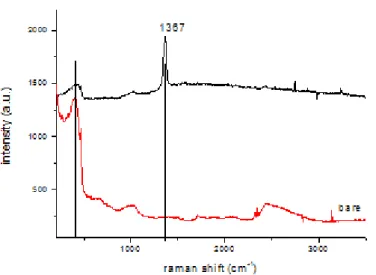
Figure 16. Raman spectra of bare steel and BN products synthesized on it showing a
peak at 1367 cm-1
After these best results are produced for the molar ratio of reactants at 4:1:1. In the above figure it is shown that these conditions together with 200 sccm NH3 flow give rise to bamboo like BNNNTs if stainless steel is used as a substrate. In order to distinguish the peaks coming from the stainless steel surface as it is and the products synthesized on it two different Raman spectra are taken. One of the spectrum belongs to bare stainless steel the other one belonging to that coated with BNNTs. Due to in plane E2g vibration mode of BN, Raman peak at 1367 cm-1 is observed.
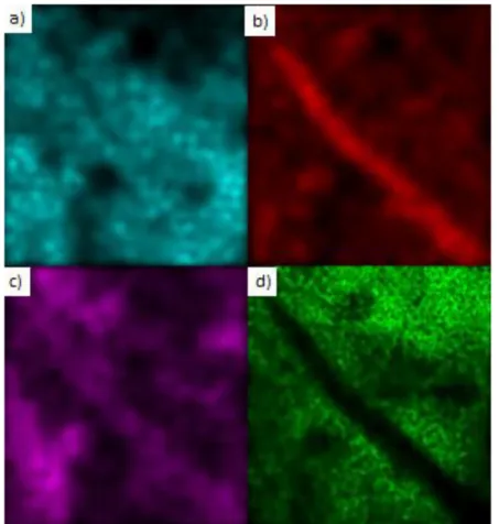
27
To investigate the morphologies of these tubes and the other probable products synthesized, SEM images are taken at different magnifications. Moreover energy dispersive X-ray spectroscopy data apparently shows that the tubular structures contain nitrogen. On the tip of the tubular structures iron is observed in an oxidized state. Together with the Raman spectra and SEM images, EDX data proves that these are BNNTs capped with oxides of iron.
Figure 17. SEM images at various scales
28
Figure 19. Raman spectra showing a peak at 1367 cm-1
Figure 20. XRD spectra for different planes of h-BN.
By varying the conditions namely doubling the flow rate of ammonia and keeping other parameters constant highly crystalline h-BN layers with an inter planar spacing approximately 0.333 Ao are observed. The usual Raman peak is seen at 1367 cm-1 proves that these h-BN layers are wrapped into tubular structures. Furthermore BNNTs are seen apparently on the SEM images. However this nanotubes have spherical other morphologies together with tubular structures.
29
Also XPS data further proves the B:N ratio near to 1 as expected in BNNTS.
Figure 22. a) Oxygen, b) Nitrogen c) Silicon d) Iron
Figure 21. XPS results give a B/N ratio of 30.9 /42.45 = 0.72 almost
30
Figure 23. a) SEM image b) overall mapping result c) elemental spectra
31
Figure 25. Raman spectrum
Another experiment that is conducted revealed interesting results. Instead of giving results in parallel with the two previously conducted at the same conditions except the flow rates of ammonia 200 and 400 sccm respectively. This run with 300 sccm mass flow of ammonia is resulted in no BNNTs production. Nevertheless there is still some observations proving the presence and production of h-BN in Raman spectrum. EDX spectrum and mapping results show that these fiber like structures are mostly composed of iron oxide
32
.
Figure 27. a) SEM image b) Nitrogen c) Oxygen d) Chromium e) Iron f) Silicon g)
33
Figure 28. Raman spectrum
It is also possible to produce BNNTs not only at 1200 C but also at 1100 oC. For this an experiment of 4:1:1 molar ratio of B, MgO and Fe2O3 respectively with an
ammonia mass flow of 200 sccm is conducted at 1100 oC. As we look at the Raman spectrum it clearly shows the presence of h-BN. This information is further supported by the results obtained from XRD spectrum as can be seen in figure 30.
34
Figure 30. SEM images at various magnifications 1100 411 200 sccm NH3
However further analysis in SEM shows the morphologies of the products synthesized. Here also occurs BNNT formation however in a lesser amount and most of those BNNTs are broken as is clearly seen from SEM images.
35
Keeping other parameters constant (as compared to the previous run) only by increasing the NH3 flow rate 50%, stainless steel surfaces denser in BNNTs are produced. Here it is shown clearly that upon increase in mass flow of ammonia gas a direct response in the amount of synthesized BNNTs are observed.
Figure 33. SEM images at various magnifications SS 300 sccm 411 1100 C
As the mass flow rate of ammonia gas is further increased amount of ammonia mass flow reached the value of 400 sccm surfaces denser in BN compounds are produced. Juxtaposition of these three experiments with their parameters reveal that the one with 300 sccm ammonia mass flow gives the best results. Parameters reveal that if
36
the NH3 amount is increased by two fold a spectra of BN compounds are produced.
However the best condition is the one with 300 sccm ammonia while 200 sccm run gives tubular structures with broken tips.
Figure 34. Raman spectrum
Figure 35. SEM images at various magnifications revealing less BNNTs production
on stainless steel 4:1:1 molar ratio, 1100 oC, 400 sccm, 400 mg reactants.
The images in figure 36 also shows the upon increase of reactants and thus increase partial pressure of intermediates the BNNT production is not possible.
37
It is possible to synthesize BNNTs even at 1000 oC using stainless steel as a substrate.
Figure 36. Raman spectrum
The Raman spectrum shows a Raman shift at 1367 cm-1 however it is very broad. Silicon peak shown gives a very sharp peak at 512 cm-1 revealing not adequate surface coverage. In SEM images at high magnification values it is clearly seen that there exist some tubular structures. However there is a spectrum of morphologies.
Figure 37. SEM images at various magnifications for 1000 oC, 4:1:1, 300 sccm NH3
38
Figure 38. Raman spectrum
39
In above figure BNNTs produced on MgO coated silica surfaces are seen. Usual Raman peak 1367 cm-1 and in addition to this top view and side view of synthesized BNNTs are given. Here the parameters are 4:1:1 molar ratio and 400 sccm NH3 flow rate with these parameters dense BNNTs are produced.
Figure 40. Raman spectrum
As the amount of NH3 that reacts with the precursors is decreased Raman spectra
shows that most of the other BN compounds are eliminated; shoulders disappear on the spectrum.
40
Figure 42. Raman spectrum
Figure 43. SEM images at various scalesMgO 1100 4:1:1 400 sccm NH3
Even it is possible to produce BNNTs at 1100 oC. However there are too many side products. In order to decrease the amounts of side products decreasing the mass flow of NH3 can be a solution.
41
Figure 44. Raman spectrum
As compared to the previous run in this case amount of NH3 is reduced by 25%. The Raman spectrum shows a sharp peak at its usual place 1367 cm-1. The decrease in mass flow of NH3 decreased the density of the BNNTs on the substrates. The side
products covering the substrate also decrease in significant manner if two Raman spectra of previous run are juxtaposed with this result.
42
Figure 45. SEM images at various magnifications for 1100 oC, 300 sccm NH3, 4:1:1
molar ratio
Figure 46. Raman spectrum
In our experiments Ni is also worked as a catalyst. Here are the results obtained. Raman spectrum shows a peak at 1367 cm-1 with various shoulders. There is a spectrum of compounds and the SEM images do not reveal a significant production of BNNTs.
43
Figure 47. SEM images of BNNTs on Ni catalysts at 1200 oC, 8:1:1, 300 sccm NH3.
The other run taking 8:1:1 molar ratio using nickel as a catalyst and at 300 sccm mass flow of ammonia it could not cover the substrate. For this Raman spectrum shows sharp Silicon peak and a faint h-BN peak. Locally at some region of the substrate surface there is a growth of BNNTs which are shown in the SEM images at various scales. Inside of these tubes there exist metal catalyst particles.
44
Figure 49. SEM image showing no BNNTs formation Ni 1200oC, 8:1:1 molar ratio, 200 sccm NH3 mass flow.
Another run working at 200 sccm ammonia mass flow results in no BNNTs production. However Raman spectrum shows the presence of h-BN. Since the molar ratio of boron atoms are higher than oxides and they are scarcely found in the mixture this may be the reason in low BNNTs production.
Figure 50. Raman spectrum shows a strong peak around 1360 cm-1 and various other weak peaks.
45
Figure 51. SEM images showing very rare covering of the substrates coated with Ni
Ni 1200 oC, 4:1:1 molar ratio, 200 sccm NH3 mass flow.
Since the production of BNNTs are locally realized and they could not cover the substrate thoroughly Raman spectrum gives a peak at 1367 cm-1 together with sharp silicon peak at 512 cm-1.
Figure 52. Raman spectrum
By decreasing the molar ratio from 8:1:1 to 4:1:1 due to the amount of B2O2 increase
which has a direct influence on the density of BNNTs produced on the catalytic surface.
46
Figure 53. SEM images at various magnifications of the Ni coated substrates 1200 o
C, 4:1:1 molar ratio, 300 sccm NH3
Figure 54. Raman spectrum shows a sharp peak at 1367 cm-1
To further analyze the effect of iron on the catalytic growth of BNNTs in addition to the stainless steel surfaces solution based iron coated surfaces are used. These surfaces also gave good results as shown on Raman spectrum. In this run 4:1:1 and
47
200 sccm ammonia flow are worked out. SEM images show dense BNNTs with various diameters.
Figure 55. SEM images at various magnifications showing BNNTs on iron coated
substrates Fe 4:1:1 molar ratio, 1200 oC, 200 sccm NH3.
Figure 56. a) Iron b) Nitrogen c) Silicon d) Oxygen e) SEM images f) overall
48
EDX data shows that these tubes are made of nitrogen and capped oxides of iron.
Contact angle measurement:
Figure 57. Contact angle values of distilled H2O on BNNT coated surfaces with
respect to time.
Wettability properties of BNNTs were investigated using 8μL double distilled water. Contact angle measurement showed that stainless steel surfaces coated with BNNTs exhibit super-hydrophobic behavior. The value of the angle slightly changes with respect to time as can be seen in the figure 54.
For the future work a strategy for the growth of BNNTs that are vertically aligned is planned. Taking into account the results obtained using different kind of catalysts and application methods of these catalysts to the substrates all of those will be used as advisory cumulative experiences for the further researches.
49
In addition to this a comparative study to understand wetting properties of both BNNTs and CNTs is planned. For this surfaces coated with both CNTs and BNNTs which are produced in our laboratory will be used.
Throughout our experiments we found some other interesting morphologies of BN compounds. These are really loopholes for some other scientific researches and investigations. Micro-tubes, nano-pots and so-called nano-mushrooms can be interesting research topics for the new researches who are going to work on these topics.
The microtubules are synthesized when mass flow of NH3 was 400 sccm and molar
ratio 4:1:1 of reactants at 1200 oC. There is still BNNTs production however they are embedded, interestingly, inside these microtubular boron nitrides.
50
Figure 59. SEM images of micro-tubes filled with nanotubes
The next SEM images show so-called nano-mushrooms. These structures are looking like premature BNNTs with transparent hats covering them which probably made of h-BN.
51
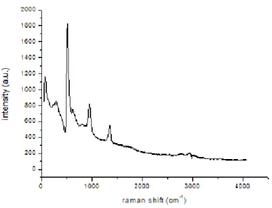
Figure 61. Raman spectrum
As we look into Raman spectrum it is very crowded nevertheless there exists a peak around 1360 cm-1.