Comparison of fully three-dimensional optical, normally
conducting, and superconducting interconnections
Haldun M. Ozaktas and M. Fatih Erden
Several approaches to three-dimensional integration of conventional electronic circuits have been pur-sued recently. To determine whether the advantages of optical interconnections are negated by these advances, we compare the limitations of fully three-dimensional systems interconnected with optical, normally conducting, repeatered normally conducting, and superconducting interconnections by showing how system-level parameters such as signal delay, bandwidth, and number of computing elements are related. In particular, we show that the duty ratio of pulses transmitted on terminated transmission lines is an important optimization parameter that can be used to trade off signal delay and bandwidth so as to optimize applicable measures of performance or cost, such as minimum message delay in parallel computation. © 1999 Optical Society of America
OCIS codes: 200.0200, 200.4650.
1. Introduction
Several approaches to three-dimensional integration of conventional electronic circuits have been pursued recently 共see Ref. 1 and references cited therein兲. Some have claimed that these developments negate the advantages of optical interconnections. In this paper we compare the utilities and the limitations of fully three-dimensional circuit layouts based on opti-cal, normally conducting, repeatered normally con-ducting, and superconducting interconnections. We show that, even if fully three-dimensional plain or repeatered normally conducting interconnections are possible, they are still inferior to optical interconnec-tions. Fully three-dimensional superconducting in-terconnections, however, are comparable with optical interconnections.
Present-day VLSI technology is a very mature technology in the sense that, for a given lithographic patterning accuracy, the interconnections on a chip are packed almost as closely as fundamental limita-tions would allow for. Little room for improvement by modification of parameters such as the aspect
ra-tios of the lines and so forth is left, since these have already been fairly optimized. Further reduction of linewidths, even if achievable, are unlikely to offer significant returns, because, at such linewidths, it is not the linewidth but heat removal and other consid-erations that limit the size and the performance of the chip.
What we refer to as a fully three-dimensional cir-cuit layout is best imagined as the three-dimensional version of a VLSI chip. Thus a fully three-dimensional VLSI “chop,” as we might refer to it, is assumed to be the three-dimensional analog of a VLSI chip in the sense that active circuits and inter-connections can occupy and be routed through three-dimensional space with the same kind of freedom and efficiency with which they are routed through 共sever-al layers of兲 two-dimensional space in VLSI chips.
A VLSI chop, as we have described it, may not be feasible in the near future, because there seems to be no effective way of manufacturing it. However, for highly interconnected circuits, the following result is of relevance2–5: Provided the interconnections are permitted to be routed through three-dimensional space, there is no disadvantage in restricting the ac-tive devices to a plane. That is, the overall volume and signal delay and the thus clock rate of a highly interconnected three-dimensional system in which the active devices are restricted to a plane will not be inferior to a system in which the active devices can be situated freely throughout the volume. This is be-cause the volume and the delays in a highly intercon-nected system are determined primarily by the space
H. M. Ozaktas共[email protected]兲 is with the Depart-ment of Electrical Engineering, TR-06533 Bilkent, Ankara, Tur-key. M. F. Erden is with Massana Ltd., 5 Westland Square, Dublin 2, Ireland.
Received 7 July 1998; revised manuscript received 30 August 1999.
0003-6935兾99兾357264-12$15.00兾0 © 1999 Optical Society of America
occupied by the interconnections so that additional restrictions on the active devices are of little or no significance. This result, which is based on purely geometrical considerations, is valid for all types of interconnection, including optical interconnections.
The above result is encouraging in that it seems to indicate that three-dimensional chops may be man-ufactured by use of the planar process to manufac-ture two-dimensional chips with a large number of wiring layers. However, it is important to realize that a many-layered chip thus manufactured will merit being called a fully three-dimensional chop only if the number of layers is comparable with the num-ber of line tracks across the horizontal extent of the chip. Otherwise, it is merely a two-dimensional chip with a large number of layers and will exhibit the general properties and limitations of two-dimensional systems. Moreover, even if the number of layers can be as great as the number of line tracks across the chip, it is possible that the quality 共capac-itance, resistance, and thus speed, density, and cou-pling兲 of vertically running lines may be inferior to horizontally running lines.
An alternative approach that has been pursued is to stack a large number of two-dimensional chips共or wafers兲 on top of one another and connect them with a grid of regularly spaced interconnections from one chip to another.6 Although such structures have been referred to as three-dimensional, they are not fully three-dimensional in the sense we have defined, because the number of chips stacked is small com-pared with the number of line tracks across the chips. However, if each chip incorporates a large number of wiring layers and if the number of chips is further increased, it is conceivable that in the near future the total number of layers in all chips may approach the number of line tracks on a single chip, and thus such systems merit being called fully three-dimensional chops. For this, however, it will also be necessary to ensure that the density, speed, and routability of ver-tical lines approach that of those confined to a single chip.
Even if unrealizable, the fully three-dimensional VLSI chop serves as an appropriate basis for comparison with optically interconnected systems, because it represents the best case for normally conducting interconnections. Since we show that optical and superconducting interconnections both of-fer performance that is superior to even this best case, the difficulty in manufacturing fully three-dimensional normally conducting chops only strengthens our conclusion.
The above discussion also applies to repeatered normally conducting interconnections. However, since repeatered lines incorporate active devices, they can be optimally utilized only if active devices are permitted on all layers. Thus the use of repeat-ers, which, as we will see, offers a significant perfor-mance advantage over plain normally conducting lines, is more demanding from a manufacturing view-point. Given this, it is not possible to make a simple argument in favor of one over the other. However,
this point will not be of concern to us, since we will show that optical and superconducting interconnec-tions are superior to both.
Having said this, it also seems necessary to clarify the realizability of fully three-dimensional optical and superconducting circuits. Fully three-dimensional su-perconducting circuits are subject to considerations similar to those of plain normally conducting circuits, apart from the fact that the materials involved are different. Thus it seems realistic to expect that sim-ilar circuit structures can be manufactured with both technologies. However, superconducting intercon-nections offer performance that is clearly superior to that of both plain and repeatered normally conduct-ing interconnections.
Optical interconnections offer performance that is superior to plain and repeatered normally conducting interconnections and that is comparable with super-conducting interconnections, if we assume similar structural and manufacturability constraints on all technologies. However, we can almost certainly get closer to full three dimensionality with optical inter-connections than with any of the other technologies; so optics emerges as the best option.
Although most people are readily willing to accept the fact that only optics will allow for fully three-dimensional circuits, there is a point in more careful justification of this as well. Our justification rests on three points. The first point is based on the pre-viously stated observation that there is nothing to be lost by constraining the active devices to lie on a plane, provided that the interconnections are able to occupy three-dimensional space. This is important because there does not seem to be an efficient and practical optical architecture that can provide inter-connections among a three-dimensional array of op-tical sources and detectors共although one approach is suggested in Ref. 7兲; most optical architectures pro-vide interconnections between planes of sources and detectors. Second, it is possible to realize arbitrary patterns of interconnections with optical interconnec-tions with the effective interconnection density as-sumed in the models we use below to show the superiority of optics.8 –10 Thus the density of optical communication is determined primarily by the den-sity of the optical sources, modulators, or detectors. This brings us to our third point. Currently, self-electro-optic effect devices flip-chip bonded to silicon chips11,12 can be spaced at least as close as 50-m apart and perhaps even closer. Although this is quite large compared with the size of an optical wave-length, in light of what is achievable today it seems fair to assume that the density of vertical connections in three-dimensional electrical technologies will not greatly exceed共if they do exceed兲 the density of this and other optical technologies so that optical inter-connections will always allow us to construct systems that are comparatively closer to full three dimension-ality.
To support our claim that optics is superior, we are relying only on optical systems’ being at least as three-dimensional as normally conducting systems
共since we show that optics is superior when both are fully three-dimensional兲. However, superconduc-tors offer performance that is comparable with optics when both are fully three-dimensional. Thus, if some kind of volume lithography or other technique allows for the construction of fully three-dimensional superconducting circuits in the future, these may contend with optical circuits. In that case the choice will be based on a number of factors not accounted for in this study, such as voltage isolation, impedance matching in the presence of multiple taps, electro-magnetic interference, etc. Finally, we add that, even solely on the basis of the considerations of this study, there are a number of circumstances in which fully three-dimensional superconducting systems may be preferable to optical ones.
2. General Considerations
Our comparison of different interconnection technol-ogies will be based on the trade-off relations between the quantities S⫽ 1兾 共inverse signal delay or laten-cy兲, B 共bit repetition rate or bandwidth兲, and N 共num-ber of devices or computing elements兲. These trade-off relations determine the largest values of S, B, and
N that are simultaneously achievable; given any two
of these parameters, we can determine the largest value attainable by the other. Another quantity of importance, denoted by H, is the bisection of the sys-tem. The bisection is the number of connections crossing an imaginary plane that divides the system into two approximately equal parts. The bisection– bandwidth product HB and the bisection–inverse-delay product HS are often more meaningful measures of performance or throughput than aggre-gate bandwidth NB or NS. It is often appropriate to model the dependence of the bisection on N by a power-law expression of the form H⫽ kNp, where
is a constant, 2兾3 ⱕ p ⱕ 1 is a measure of the con-nectivity of the system共larger p means greater con-nectivity兲, and k is the average number of connections per element.13 关We can let k be absorbed in the def-inition of but prefer not to do so. As defined, is given in terms of p by ⫽ 共p ⫺ 2兾3兲⫺1共p ⫹ 1兾3兲⫺1兴. Yet another interesting quantity that is of impor-tance in certain contexts is the first-to-last bit mes-sage delayL⫽ ⫹ L兾B, where L is the bit length of
a message共for definitions of all symbols used, please see Appendix A兲.
We assume that the system consists of N primitive elements or devices each of size dd, arrayed in the form of a three-dimensional N1兾3⫻ N1兾3⫻ N1兾3grid. The grid spacing will be denoted by d and the linear extent of the system byᏸ ⫽ N1兾3d. We further as-sume that there is an average of k connections per element and that the average length of each connec-tion in grid units is r. Each logical connection may be realized with ⱖ 1 physical interconnections to increase the bandwidth B.
Heat-removal considerations imply that a system dissipating a total power ᏼ must have a minimum cross-sectional area of at leastᏼ兾Q, where Q is the maximum amount of power that can be removed per
unit area.14 This implies that the linear extent of the systemᏸ be at least ᏸ ⫽ 共ᏼ兾Q兲1兾2.
Three basic considerations apply to all interconnec-tion media. The total volume occupied by the ele-ments is Ndd3. The total volume occupied by the interconnections is kNrdW2, since kN is the total number of physical connections, rd is their average length in physical units, and W2 ⫽ A is the cross-sectional area of an interconnection. Heat-removal considerations imply a volume of at least共ᏼ兾Q兲3兾2⫽ 共kNBE兾Q兲3兾2, where E denotes the energy per trans-mitted bit, since there are kN connections, each dis-sipating power BE. Thus the linear extent of the systemᏸ ⫽ N1兾3d must satisfy
ᏸ3⫽ Nd3⫽ max关d
d3N, krW2Nd,共kEB兾Q兲3兾2N3兾2兴. (1) It is known that the bisection and the average con-nection length of a system are closely related. If the bisection can be modeled as kNp, then the average connection length is r ⫽ Np⫺2.13 Inserting this into the above, we obtain
ᏸ ⫽ N1兾3d⫽ max关d
dN1兾3,共k兲1兾2WNp兾2,共kEB兾Q兲1兾2兴. (2) Further progress requires the introduction of physi-cal interconnection models, which we do below.
3. Interconnection Models
The interconnection models used are summarized in Tables 1– 4 below. Their justification and derivation have been given elsewhere2共also see Refs. 15 and 16 for further references兲. These models are simply re-lations between the external parameters of intercon-nections, which are
1. Interconnection length l.
2. Cross-sectional area A or transverse linear ex-tent W, where A ⫽ W2. These parameters define packing density and thus include any necessary line-to-line separations.
3. Signal delay, which is given by the greater of the propagation delay Tpand the minimum temporal pulse width T, which in turn is the greater of a line-imposed component Tland a device-imposed compo-nent Td:
⫽ max共Tp, T兲, T⫽ max共Tl, Td兲.
4. Minimum pulse repetition interval Tr, which is usually equal to T, the minimum temporal pulse width along the interconnection
Tr⫽ T.
5. The energy per transmitted bit, E.
The relationships in Tables 1– 4 represent a full char-acterization of the physical properties of the intercon-nections, as far as this study is concerned. All other
internal parameters that are commonly used to
char-acterize such lines, such as transverse aspect ratio, capacitance, resistance, etc., are assumed to be set共at least approximately兲 to their optimal values in the derivation of these models and thus do not appear in these models.
For optical interconnections 共Table 1兲 the cross-sectional area is taken to be proportional to the wave-length squared: A ⫽ W2 ⫽ 共 f 兲2, where the constant f can be as small as ⬃1 for a diffraction-limited system but may be larger in practice. 共It is important to note that for certain classes of optical interconnection architectures, which we collectively refer to as multifacet architectures, f is not a constant but increases with N. Such architectures are clearly
undesirable. See Refs. 7–10 for further discussion.兲 The signal delay is taken to be the greater of the speed-of-light delay and the device rise time: ⫽ max共l兾c, Td兲. Since the effects of dispersion and at-tenuation can be made small for the length scales in consideration, T⫽ Trand E are assumed to be con-stants. This model is valid for free-space intercon-nections as well as guided-wave interconintercon-nections, although the value of f can be much smaller with free-space interconnections.8
In Table 2 we see the relationships tying the length, cross-sectional area, delay, and energy for normally conducting lines for the case Tdⱕ Tl. The
symbols, ⑀, , and v ⫽ 共⑀兲⫺1兾2denote the resistivity of the conductor, permittivity and permeability of the dielectric, and propagation velocity in the dielectric, respectively. V denotes the nominal voltage level.
What is unique to our model is that it intrinsically accounts for the proper scaling effects that are due to the skin effect and deals with unterminated RC lines and transmission lines in a unified manner. One conclusion that may be derived on careful inspection of our model is that the use of many narrow lines is not more beneficial than a single wide line in terms of increasing information density. 共Use of a single wide line amounts to setting ⫽ 1.兲 Yet another conclusion is that it is beneficial to photographically scale down interconnection-density-limited layouts until we are in the unterminated region. After this, further reduction in scale does not further improve system signal delay. 共This conclusion is related to a well-known argument stating that the rise time of a
RC line remains constant when all of its dimensions
are downscaled.兲
The use of active repeater devices along the line changes the relationship for delay versus linewidth
Table 1. Optical Interconnection Modelawhen T
l< Td< Tp
W T⫽ Tr E
f ⫽ constant l兾c Td⫽constant constant aThe delay ⫽ T
pis a function of length l only. The pulse width
T⫽ Tdand the energy E are assumed independent of length l and
width W.
Table 2. Normally Conducting Interconnection Modelawhen T
d< Tl T⫽ Tr E Termination W2ⱕ 16⑀vl 16⑀ l 2 W2 16⑀ l2 W2 2⑀V2l no W2ⱖ 16⑀vl l v 16⑀ l2 W2 2⑀V2vT yes aThe delay ⫽ max共T, T
p兲, pulse width T ⫽ max共Tl, Td兲, and
energy E are given as functions of length l and width W. Tp⫽ l兾v
is the propagation delay. The final column indicates whether the line is to be terminated in that region.
Table 3. Repeatered Interconnection Modela
T⫽ Tr E Termination W ⱕ 4
冉
R0C0 冊
1兾2 4共R0C0⑀兲1兾2 l W R0C0⫽ constant 2⑀V 2l no W ⱖ 4冉
R0C0 冊
1兾2 公⑀ l R0C0⫽ constant 8⑀V 2冉
R0C0 冊
1兾2 l W yesThe delay, pulse width T, and energy E are given as functions of length l and width W. The final column indicates whether the stages of the line are to be terminated in that region.
Table 4. Superconducting Interconnection Model when Td< Tp共Td< Tlin the Unterminated Case兲 a T⫽ Tr E Termination W ⱕ 4V Jsc
冑
兾⑀ 16⑀Vp Jsc l W2 16⑀Vp Jsc l W2 2⑀V2l no 4V Jsc冑
兾⑀ ⱕ W ⱕ 4p 4p v l W Td⫽ constant 2冑
⑀ V 2 W 4p Td yes Wⱖ 4p l v Td⫽ constant 2冑
⑀ V 2T d⫽ constant yesThe delay ⫽ max共Tp, T兲, pulse width T, and energy E are given as functions of length l and width W. The final column indicates
as shown in Table 3. R0C0 denotes the intrinsic delay of the repeating devices. The optimal number of repeaters 共which may be zero兲 is used at optimal spacings for each line.17
Table 4 is for superconducting lines. Our models take into account the proper scaling effects associated with the superconducting penetration depthp and the critical current density Jsc. A conclusion that can be derived on careful examination of the table is that for wire-limited layouts it is optimal to scale down the system until we are in the intermediate region共the second line of the table兲.
We will assume the following in our numerical ex-amples: f ⫽ 10 m, c ⫽ 3 ⫻ 108m兾s, Td⫽ 100 ps, E⫽ 1 pJ, V ⫽ 1 V, ⫽ 0.0274 ⍀ m 共aluminum兲, ⑀ ⫽ 3.9⫻ 8.85 ⫻ 10⫺3f F兾m 共silicon dioxide兲, ⫽ 4 ⫻ 10⫺7H兾m 共nonmagnetic materials兲, v ⫽ 1.52 ⫻ 108 m兾s, R0C0 ⫽ 100 ps, p ⫽ 0.2 m, and Jsc ⫽ 50 mA兾m. 4. Analysis A. Optical Interconnections
In the case of optical interconnections, W and E are taken as constants. Assuming that Tddoes not dom-inate the propagation delay S ⫽ 1兾 ⫽ 1兾共l兾c兲 ⫽ 1兾共ᏸ兾c兲 ⫽ c兾ᏸ, the trade-off relation between S, B, and N is obtained from Eq.共2兲 as
1 S⫽ 1 cmax关ddN 1兾3,共k兲1兾2共 f 兲Np兾2,共kEB兾Q兲1兾2N1兾2兴, ⫽ max共1, BTd兲. (3)
Clearly, we choose to be equal to B兾共1兾Td兲 when this ratio is greater than 1 to support that value of B, but of course we cannot have less than one channel even if this ratio is less than 1. This relationship defines a surface in the three-dimensional parameter space defined by S, B, and N. By examining this relation-ship, we can tell the price we have to pay in terms of a decrease in one or two of these parameters to in-crease the remaining one共s兲. Note that there are several regions that might be referred to as the element-size-limited region共when the first term dom-inates兲, the interconnection-density-limited region 共when the second term dominates兲, and the heat-removal-limited region 共when the third term domi-nates兲.
B. Normally Conducting Interconnections
Unlike with optical interconnections where W is con-stant, with normally conducting interconnections we are free in choosing W, provided it exceeds a certain minimum manufacturable value Wmin. If ddis small and heat removal is not an issue, we would prefer to set W to this minimum so as to make d and the overall system as small as possible. However, the minimum manufacturable value of W is not the only determinant of how small the system can be made. If element size or heat removal require that we set ᏸ3
⫽ Nd3
⬎ kNrdWmin 2
, we will agree to increase W
until Nd3⫽ kNrdW2. 共If d and hence the lengths of the lines are already set by factors other than inter-connection density, we increase W so as to fill up available space. In this way we reduce the resis-tance of the lines as much as possible. Keeping the lines narrow while we have extra space around is clearly suboptimal.兲 We also assume that device de-lays Td are small so that T⫽ Tl.
Thus, using d2 ⫽ krW2, l ⫽ ᏸ ⫽ N1兾3d, and the interconnection model, we obtain
T⫽ 共16⑀兲共kr兲N2兾3, (4)
and the maximum value of B satisfies B⫽ 1兾T or
BNp⫽ 共16⑀兲⫺1共k兲⫺1, (5) an expression in which S does not appear. By defi-nition, S⫽ 1兾 may never exceed 1兾max共Tl, Td, Tp兲 ⫽ 1兾max共Tl, Tp兲 ⫽ 1兾max共T, Tp兲. Thus the above re-lation for B may be used to find S⫽ 1兾max共1兾B, Tp兲 ⫽ min共B, 1兾Tp兲. From Table 2 we see that the con-dition for Tp⬍ T is W
2
⬍ 16⑀vl. As we scale down the system photographically, all linear dimensions are decreased in proportion. Thus, below a certain critical W, this condition is satisfied so that propaga-tion effects need not be considered, and we have en-sured that S is not worse than B.
However, a number of factors may be an impedi-ment to downscaling. First, our lithographic accu-racy may not enable us to pattern lines sufficiently fine. This is not an issue with the availability of submicrometer scaling. Second, the system cannot be made smaller than dictated by the size of the elements N1兾3dd. This is also not a limitation in highly connected systems with a large number of el-ements. Finally, heat-removal limitations may pre-vent us from scaling the system down sufficiently.
For typical parameter values two-dimensional lay-outs may be downscaled to the extent that propaga-tion effects need not be considered on the longest line 共i.e., Tp⫽ l兾v ⬍ T兲 so that S is simply equal to B.2 To understand this, note that T does not depend on the scale of the system as measured by the value of the grid spacing d. However, the propagation delay along the longest line Tp⫽ N1兾3d兾v depends linearly on d. Thus, as we downscale the system by reducing
d, eventually Tpwill fall below T, and Tpwill not be a limiting factor in determining and S. This may not be possible for three-dimensional layouts, espe-cially for room-temperature voltages. This is be-cause we cannot downscale the system below a certain value of d and still be able to remove the dissipated heat. Thus the propagation delay Tpmay remain larger than T, and thus the value of S may be quite less than the value of B. This is the essential qualitative difference between two-dimensional sys-tems and three-dimensional syssys-tems.
Now we give a complete analysis of the effects of heat removal, enabling us to determine the scale of the system as set by heat-removal considerations. We will assume that pulses of identical temporal width are launched into all lines regardless of their
length. Thus the minimum value of this pulse width is set by the longest connection. 共In principle, there is nothing that stops us from launching shorter pulses into the shorter lines, resulting in some energy savings. The following analysis may be modified for this case if such an approach is deemed practical.兲 The minimum pulse width for the longest line is given by
T⫽ 共16⑀兲 l
2
W2, (6)
with l⫽ ᏸ. The above expression for T is indepen-dent of the scale of the system. This is because both
l and W will change by the same factor when the
system is scaled. Pulses of this duration are emitted into lines of all lengths. According to our intercon-nection model, the shorter lines, for which Tⱖ Tp, will be left unterminated, whereas the longer lines, for which T ⬍ Tp, will be terminated. 共On termi-nated lines, several pulses of length T might simul-taneously be in transit along the line.兲 Let us denote the break-even length for termination共in grid units兲 as rx. Thus lines for which rxd兾v ⱕ T will be left
unterminated and those for which rxd兾v ⬎ T will be
terminated. If the length N1兾3d of the longest line in our system satisfies N1兾3d ⱕ Tv, all lines will be
unterminated.
The problem is that initially we do not know d, which depends on the total power dissipated, which in turn depends not only on d but also on what frac-tion of the lines are unterminated. Let us assume initially that N1兾3d ⱕ Tv so that all lines are
unter-minated. Then the average energy per bit is given by 2⑀V2rd, the power dissipation by 2⑀V2rdB, and the
total power dissipation by kN2⑀V2rdB. This must be less than the cross-sectional area of the system
N2兾3d2times Q. Thus
dⱖ2⑀V
2kNp⫺1兾3B
Q . (7)
Now, if indeed N1兾3d ⱕ Tv, justifying our assump-tion, we are done and d is given by relation 共7兲. If not, this means that some of the longer lines will be terminated, for which the energy per bit is given by 2⑀V2vT. Then the total power consumption and heat-removal condition may be expressed in terms of a piecewise integral QN3兾2d2ⱖ
冋
兰
1 rx 2⑀V2rdg共r兲dr ⫹兰
rx N1兾3 2⑀V2vTg共r兲dr册
B, (8) where g共r兲 is the line-length distribution,2,3given ap-proximately by g共r兲 ⬇ 共⫺d兾dr兲关kr3共 p⫺1兲共1 ⫺ r3兾N兲兴 for the analytical form of the bisection we have assumed. The first integral represents the power dissipated on the unterminated lines, and the second representsthe power dissipated on the terminated lines. Eval-uating the above, we find
Qd2ⱖ N1兾3k关2⑀V2r
x
3p⫺2d⫹ 2⑀V2vTr
x
3共 p⫺1兲z兴B, (9) where zⱕ 1 is a factor whose exact form will not be important. Now, using rx ⫽ vT兾d, it is possible to
solve for d as
d3p⫺1ⱖ2⑀V
2共vT兲3p⫺2kN1兾3B
Q , (10)
where, since zⱕ 1, we replaced ⫹ z ⯝ with little error. Note that this expression forms continuity with relation 共7兲 at N1兾3d ⫽ vT. Thus, combining
the two expressions, we may write the minimum in-terelement spacing d as set by heat removal in the form d⫽ min
再
2⑀V 2 kNp⫺1兾3B Q ,冋
2⑀V2共vT兲3p⫺2kN1兾3B Q册
1 3p⫺1冎
. (11) The virtue of this equation is that it combines com-pactly all possible cases. Finally, the signal delay is given by 1兾S ⫽ max共N1兾3d兾v, N1兾3dd兾v, T兲.
C. Repeatered Interconnections
First, assume that element size and heat removal need not be considered. Using ⫽ 4共R0C0⑀兲1兾2l兾W,
l⫽ N1兾3d, and d2 ⫽ krW2, we obtain
SNp兾2⫽ 关4共R
0C0⑀兲1兾2兴⫺1共k兲⫺1兾2,
⫽ max共1, BR0C0兲, (12)
where we assumed that the system has been down-scaled sufficiently so that Wⱕ 4共R0C0兾兲1兾2. This relation is similar to the corresponding relation for optical communication in form 关the second term of Eq.共3兲兴.
Equation 共12兲 is scale independent when W ⱕ 4共R0C0兾兲1兾2, as we have assumed to be the case 共W ⱕ 5 m for the assumed parameter values兲. When element size is accounted for, S is given by the minimum predicted by Eq. 共12兲 and 1兾S ⫽ 公⑀N1兾3d
d.
When heat-removal considerations are taken into account, it may be the case that it is not possible to downscale the system so that W ⱕ 4共R0C0兾兲1兾2. In this case it is possible to show that the minimum value of d is given by d⫽ min
再
2⑀V 2kNp⫺1兾3B Q ,冋
8⑀V2共R 0C0兾兲1兾2 Q册
1兾2 ⫻ 1兾4共k兲3兾4N3p兾4⫺1兾3B1兾2冎
. (13) Thus the resulting delay is the greater of公⑀N1兾3d with d given above,公⑀N1兾3dd, and that given by Eq. 共12兲.
D. Superconducting Interconnections
As with normal conductors, we agree to choose W so that the condition d2 ⱖ krW2 is always satisfied with equality. Mostly we will be at an advantage 共because of the inverse dependence of on W for given
l兲, and never at a disadvantage, by doing so.
When we refer to Table 4, some reflection reveals that if dd is small and heat removal need not be considered, it is optimal to work in the intermediate region, assuming we can manufacture Wⱕ 4p. 共To see this, note that, as we scale the system photo-graphically, l varies in linear proportion to W.兲 As-suming Td is small, an analysis similar to that for repeaters results in
SNp兾2⫽
冉
v 4p冊
共k兲⫺ 1兾2,
⫽ max共1, BTd兲. (14)
This relation is independent of the specific choice of
W, provided that it lies between 4V兾共Jsc公兾⑀兲 and
4p.
Heat removal has no effect on performance unless it requires that d be large enough that Wⱖ 4p. The analysis and the results are similar to the optical case, provided that we replace the energy E4 2V2公⑀兾Td: 1 S⫽ 1 vmax关ddN 1兾3,共k兲1兾2共4 p兲Np兾2, 共k2V2
冑
⑀兾 T dB兾Q兲1兾2N1兾2兴, ⫽ max共1, BTd兲. (15)If low voltage values are used, this energy can be much less than ever achievable with optical intercon-nections.
5. Comparisons
A. Qualitative Comparisons
For optical and superconducting interconnections there is no upper limit to B for any value of N. One can simultaneously choose N and B arbitrarily large. Thus one can also increase the bisection– bandwidth product HB ⫽ kNpB arbitrarily, at the expense of
greater signal delay共smaller S兲. The value of S cor-responding to a given value of B and N may be found from Eq.共3兲 or Eq. 共15兲. A particularly simple trade-off between bisection– bandwidth product HB and S is obtained when interconnection density is the dom-inating consideration 共the second term in Eq. 共3兲 or Eq.共15兲兴:
S共HB兲1兾2⫽ constant. (16)
The bisection–inverse-delay product HS can also be determined from Eq.共3兲 or Eq. 共15兲. Assuming ddis small, we can show
HS⬀N
p⫺1兾2
B1兾2 , (17)
from which we see that this measure of performance can also be increased without bound.
For normally conducting interconnections, B is re-lated to N through Eq.共5兲 so that, for a given value of
N, it is not possible to increase B beyond that dictated
by this equation. This is in contrast with the optical and the superconducting cases where B could be ar-bitrarily increased. Any attempt at increasing B by using wider lines or ⬎ 1 parallel channels is thwarted by the increase in line lengths, since T ⬀
l2兾W2. We further see that the bisection– bandwidth product is a constant and cannot be in-creased beyond a certain value:
HB⫽ constant. (18)
Thus even when we assume very fast devices共Td
neg-ligible兲, negligible element size dd, arbitrarily small manufacturable linewidths Wmin, a fully
three-dimensional layout, and ignore the effects of heat re-moval, we still find that there is a fundamental upper limit to the bisection– bandwidth product for nor-mally conducting interconnections.
We have seen that, because heat removal may not allow for such systems to be scaled down sufficiently, the inverse delay S may be even smaller than B. Thus the bisection–inverse-delay product HS may be even more inferior than the bisection– bandwidth product HB. The use of normal conductors is inhib-itive for applications for which these products are suitable figures of merit.
The behavior of repeatered systems is similar to that of optical and superconducting systems, when heat removal is not considered. However, the situ-ation is worse when heat removal is considered. We refer to Eq.共13兲, which accounts for the effects of heat removal. For large N and B, the second term in this equation will be applicable so that d⬀ r3兾4B3兾4N1兾6, which is larger than d⬀ r1兾2B1兾2dictated by intercon-nection density considerations. Thus the resulting growth rate of signal delay becomes ⬀ r3兾4B3兾4N1兾2, which is worse than ⬀ B1兾2N1兾2, which we found in the optical case. For given B the growth rate of the bisection–inverse-delay product is then found to be
HS⬀ Np兾4, (19)
which is inferior to the optical HS⬀ Np⫺1兾2共since p ⬎ 2兾3兲. If we do not terminate each stage of the repeaters individually and charge up the segments, as would most likely be the case in practice, then the first term in Eq. 共13兲 becomes applicable so that ⬀ rBN2兾3. In this case we find that, for given B, the bisection–inverse-delay product is bounded from above and cannot be increased with increasing N, an inhibiting situation.
B. Quantitative Comparisons
There are many ways to present quantitative com-parisons of S–B–N surfaces for different interconnec-tion media. First, we will plot S as a function of N
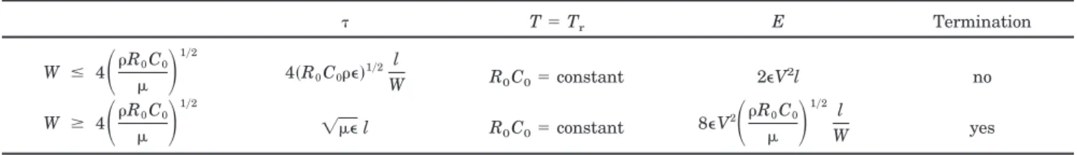
for the four media, with B set to the largest value allowed for by normally conducting interconnections for each value of N关as given by Eq. 共5兲; For the three other media, B can be specified independently. However, since this is not the case for normal con-ductors, choosing B in this manner allows for a fair comparison of the values of S that correspond to the same values of N and B.兴 S, B, and N are related by Eq.共3兲 for optics and by Eq. 共15兲 for superconductors. For repeaters the relation between S, B, and N is calculated as described by the comment following Eq. 共13兲. For normal conductors S is determined as a function of N as described by the comment following Eq.共11兲. We see in Fig. 1 that the decrease of S with increasing N occurs more slowly with optical and superconducting interconnections so that they are su-perior for larger values of N. For lower values of N, repeatered interconnections may offer superior or comparable values of S.
On comparison of the coefficients of Eq.共12兲 and the second term of Eq.共3兲, we see that repeaters are comparable with optics in terms of interconnection density considerations, but the picture changes when heat-removal considerations are accounted for.
We also note that Eq.共15兲 is identical in form to Eq. 共3兲 derived for optical interconnections. The numer-ical factors are also comparable, as is also evident from Fig. 1. We stress that, despite the similarity of the final relations, the physics involved is quite dif-ferent. The scale of the optical system is fixed, whereas the scale of the superconducting system may be reduced, resulting in much smaller system size 共this does not result in greater performance though, since the reduction in line lengths is precisely can-celed by the inverse dependence of the delay on W.兲
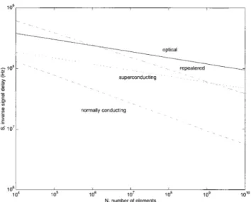
An alternative comparison is provided in Fig. 2, whose four panels each correspond to a different 共con-stant兲 value of B, constituting sections of the S–B–N
space. The comments made for the previous figure hold in this case as well. Note, however, that the curve for normal conductors terminates at a certain value of N, reflecting the fact that information cannot be transmitted at the indicated value of B beyond that value of N, regardless of the value of S.
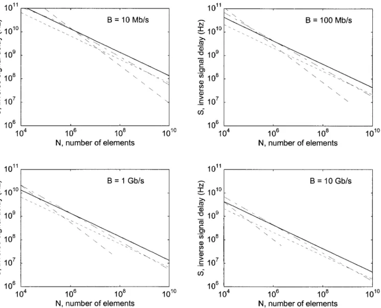
We have also examined the effect of reducing the nominal voltage value V from 1 V down to 0.1 and 0.01 V, which may be possible at lower temperatures共the improvements saturate near the lower level, and fur-ther improvements are not obtained for even lower voltages兲. Since the energy dissipation for the three conducting technologies will also be consequently re-duced, this is expected to alter the comparison in favor of these technologies. From Fig. 3 we see that this is indeed the case, especially for higher values of B for which the dissipated power is higher. All three con-ducting technologies are able to offer much higher val-ues of S; however, the curve for normal conductors still terminates at a certain value of N: The fact that in-formation cannot be transmitted at the indicated value of B beyond that value of N is not based on heat-removal considerations and so is not alleviated by a reduction of the voltage level. Reduction of the volt-age level makes superconductors look especially at-tractive. It is important to note that in this figure we have assumed the reduction in voltage to have no effect on optical interconnections. However, it is likely that a reduction of temperature and voltage will also reduce the energy per transmitted bit for optics. If the reduc-tion in energy is, for instance, 10, the curves for optics should simply be moved upward by公10 in Fig. 3.
Finally, we discuss the effect of varying p. Choosing larger values of p favors optics and superconductors, whereas choosing lower values of p has the opposite ef-fect. The values of p for problems requiring global in-formation flows, such as sorting, permutation and interconnection networks, discrete Fourier transforms, and global filtering, are usually close to unity. In other words, the bisections are proportional to N. The value of p⫽ 2兾3 represents complete locality in three dimen-sions. The value p⫽ 0.8 used in our numerical exam-ples thus represents an intermediate value.
C. Optimal Operating Point on the S–B–N Surface
In Fig. 1 we set B to its largest possible value for normal conductors, as determined by Eq. 共5兲. Of course, it is not necessary to transmit bits along the lines at this maximum possible rate; one can transmit bits at lower rates as well 共as is the case in Fig. 2兲. Referring back to Eq.共11兲, we see that if we choose B to be smaller, d will be smaller, resulting in larger values of S. Thus we see that there is a trade-off between S and B. If we set B to its largest possible value of B⫽ 1兾T, this will result in a particular value of S, as shown above. However, by choosing B to be smaller共i.e., by operating at a smaller duty ratio兲, we can reduce power dissipation, pack the elements more densely共i.e., reduce d兲, and thus decrease propagation delays, resulting in a larger value of S. 共There is no purpose in reducing B beyond a certain extent, how-ever, since once the scale of the system is reduced to
Fig. 1. Comparison of optical共solid curve兲, normally conducting 共dashed curve兲, repeatered 共dotted–dashed curve兲, and supercon-ducting interconnections共dotted curve兲. We take k ⫽ 5, p ⫽ 0.8,
Q⫽ 10 W兾cm2and assume d
d, Td, and Trto be small enough to
the extent that all lines become unterminated, further reduction in scale will not improve S. There is an upper limit to both quantities S and B regardless of the other; however, they can be traded off for each other over a certain range.兲 Given any optimization func-tion involving B and S, we can find the optimum duty ratio and the associated values of S and B.
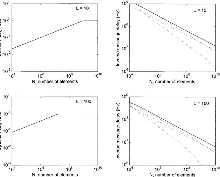
As a first example, let us assume that we would like to maximize S⫽ B 共that is, maximize S and B under the constraint that they are equal兲. This optimiza-tion funcoptimiza-tion might be appropriate for a synchronous system whose clock rate is set by the signal delay along the longest connection. The duty ratio will be denoted by x ⱕ 1 so that the bit repetition rate may be expressed as B ⫽ x兾T. In Fig. 4共a兲 we plot the optimum duty ratio x that maximizes S ⫽ B. We observe that rather small duty ratios are optimal for a wide range of N.
A similar trade-off between S and B exists for the other interconnection media as well. Figure 4共b兲 shows the resulting comparison of the four media
when the duty ratio is chosen such that S ⫽ B is maximized. Despite the fact that the asymptotic su-periority of optical and superconducting interconnec-tions remains and similar break-even values are observed, the performance offered by repeatered in-terconnections is much more comparable with that offered by optics and superconductors in this exam-ple. The major strength of optics and superconduc-tors is their ability to provide large values of N and B simultaneously with minimal sacrifice in terms of S. Thus their superiority is less pronounced when S is emphasized as strongly as or more strongly than B.
We now consider a second example. In certain parallel computing contexts, it is the case that one desires to minimize the first-to-last bit communica-tion latencyLof L bit messages, given by
L⫽ ⫹ L B⫽ 1 S⫹ L B. (20)
Fig. 2. Comparison of optical共solid curve兲, normally conducting 共long-dashed curve兲, repeatered 共long–short-dashed curve兲, and super-conducting interconnections共short-dashed curve兲. We take k ⫽ 5, p ⫽ 0.8, Q ⫽ 10 W兾cm2and assume d
d, Td, and Trto be small enough
The trade-off relations we have derived between S and B allow us to find the optimum operating point resulting in the smallest value of L and also to
compare the resulting values ofLfor the different media. The results are shown in Fig. 5. Although this example does not add significant new informa-tion with regard to the comparison of the technolo-gies, it serves to illustrate the usefulness of our models and analysis in obtaining quantitative re-sults.
An alternative discussion of related issues may be found in Refs. 18 and 19.
6. Conclusions
In this paper we have compared hypothetical fully three-dimensional normally conducting, repeatered normally conducting, superconducting, and optical systems. We find that optical and superconducting interconnections are comparable with each other and superior to the others. Since optics seems to allow
Fig. 3. Comparison of optical共solid curve兲, normally conducting 共long-dashed curve兲, repeatered 共long–short-dashed curve兲, and super-conducting interconnections共short-dashed curve兲. Similar assumptions are made as in the previous figures. 共a兲 B ⫽ 100 Mbit兾s, V ⫽ 0.1 V;共b兲 B ⫽ 100 Mbit兾s, V ⫽ 0.01 V; 共c兲 B ⫽ 10 Gbit兾s, V ⫽ 0.1 V; 共d兲 B ⫽ 10 Gbit兾s, V ⫽ 0.01 V.
Fig. 4. Comparison of optical共solid curve兲, normally conducting 共dashed curve兲, repeatered 共dotted–dashed curve兲, and supercon-ducting interconnections共dotted curve兲 when S ⫽ B is maximized. Similar assumptions are made as in the previous figures, but Td⫽
us to approach full three dimensionality more closely, it represents the most superior option.
It is important to understand that none of the in-terconnection media we have considered enables con-tinual reduction of signal delay by downscaling. 共Optical interconnections cannot be downscaled, and all kinds of conducting interconnections exhibit an inverse dependence of delay on linewidth, below a certain linewidth.兲
In discussing the limitations of conducting inter-connections, we allowed for arbitrarily small scaling and arbitrarily fast devices. We saw that normal conductors, whether terminated or not, did not allow for B to be kept constant with increasing system size 共which is possible with the other media兲. Both B and S were found to decrease sharply with increasing
N. The bisection–inverse-delay and bisection– bandwidth products were found to be bounded from above. This is in contrast to the other media with
which it is possible to arbitrarily increase B and the bisection– bandwidth product for any given N.
Repeaters are inferior to optics and superconduc-tors, since they result in faster growth of signal delay and slower growth of the bisection–inverse-delay product with increasing N.
Optical and superconducting interconnections lead to similar performance for similar communica-tion energies. Although superconducting layouts may be much smaller than optical layouts, they do not result in smaller delay because of the inverse dependence of delay on linewidth, once conductor thickness drops below the penetration depth. Op-tical interconnections may allow us to more closely approach full three dimensionality and offer free-dom from termination problems. Superconductors may offer much lower energies, especially if the voltage level is reduced. This in turn might enable reduction of signal delay.
Fig. 5. Comparison of optical共solid curve兲, normally conducting 共long-dashed curve兲, repeatered 共long–short-dashed curve兲, and super-conducting interconnections共short-dashed curve兲 when Lis minimized. Similar assumptions are made as in the previous figures, but
Td⫽ 100 ps. 共a兲 Optimum duty ratio for L ⫽ 10. 共b兲 Resulting L⫺1versus N for L⫽ 10. 共c兲 Optimum duty ratio for L ⫽ 100. 共d兲
Appendix A: Definitions of Symbols Used
S inverse signal delay⫽ 1兾,
B bit repetition rate共bandwidth兲,
N number of devices or elements,
H bisection of the system⫽ kNp,
HB bisection– bandwidth product,
HS bisection–inverse-delay product,
k average number of connections per element,
p system connectivity measure共Rent exponent兲, ⫽ 共p ⫺ 2兾3兲⫺1共p ⫹ 1兾3兲⫺1,
dd linear size of each device or element,
d grid共lattice兲 spacing of the layout, ᏸ linear extent of the system ⫽ N1兾3d,
r length of an interconnection in grid units 共dimen-sionless兲,
r average connection length in grid units ⫽ Np⫺2兾3,
number of physical interconnections per logical con-nection,
ᏼ total power dissipated by the system,
Q maximum amount of power that can be removed per unit area,
l length of an interconnection in physical units⫽ rd,
W transverse linear extent of an interconnection,
A cross-sectional area of an interconnection⫽ W2,
signal delay 共latency兲 ⫽ max共Tp, T兲,
Tp propagation delay along an interconnection,
T minimum temporal pulse width⫽ max共Tl, Td兲,
Tl line-imposed component of T,
Td device-imposed component of T,
Tr minimum pulse repetition interval, usually⫽ T,
E energy dissipated per transmitted bit,
Wmin minimum manufacturable value of W,
optical wavelength,
c speed of light in free space,
f effective f-number of optical interconnection sys-tem,
resistivity of conductor, ⑀ permittivity of dielectric, permeability of dielectric,
v propagation velocity in dielectric,
V nominal voltage level,
R0C0 intrinsic delay of a repeater,
p superconducting penetration depth,
Jsc superconducting critical current density.
We acknowledge the benefit of discussions with Volkan H. O¨ zgu¨z of Irvine Sensors Corporation, Costa Mesa, California, and Sadık C. Esener of the University of California, San Diego, California.
References
1. IEEE, eds., Proceedings of the 45th Electronic Components and Technology Conference 共ECTC兲 共Institute of Electrical and Electronics Engineers, Piscataway, N.J., 1995兲.
2. H. M. Ozaktas and J. W. Goodman, “The limitations of inter-connections in providing communication between an array of points,” in Frontiers of Computing Systems Research, S. K. Tewksbury, ed.共Plenum, New York, 1991兲, Vol. 2, pp. 61–130. 3. H. M. Ozaktas, “A physical approach to communication limits in computation,” Ph.D. dissertation 共Stanford University, Stanford, Calif., 1991兲.
4. A. L. Rosenberg, “Three-dimensional VLSI: a case study,” J. Assoc. Comput. Mach. 30, 397– 416共1983兲.
5. F. T. Leighton and A. L. Rosenberg, “Three-dimensional circuit layouts,” J. Comput. Sys. Sci. 15, 793– 813共1986兲.
6. M. J. Little and J. Grinberg, “The 3-D computer: an inte-grated stack of WSI wafers,” in Wafer-Scale Integration 共Klu-wer, New York, 1988兲, Chap. 8.
7. H. M. Ozaktas, Y. Amitai, and J. W. Goodman, “A three di-mensional optical interconnection architecture with minimal growth rate of system size,” Opt. Commun. 85, 1– 4共1991兲; errata 88, 569共1992兲.
8. H. M. Ozaktas and J. W. Goodman, “Lower bound for the communication volume required for an optically intercon-nected array of points,” J. Opt. Soc. Am. A 7, 2100 –2106共1990兲. 9. H. M. Ozaktas, Y. Amitai, and J. W. Goodman, “Comparison of system size for some optical interconnection architectures and the folded multi-facet architecture,” Opt. Commun. 82, 225– 228共1991兲.
10. H. M. Ozaktas and D. Mendlovic, “Multistage optical intercon-nection architectures with least possible growth of system size,” Opt. Lett. 18, 296 –298共1993兲.
11. K. W. Goossen, J. E. Cunningham, and W. Y. Jan, “GaAs 850 modulators solder-bonded to silicon,” IEEE Photonics Technol. Lett. 5, 776 –778共1993兲.
12. K. W. Goossen, J. A. Walker, L. A. D’Asaro, S. P. Hui, B. Tseng, R. Leibenguth, D. Kossives, D. D. Bacon, D. Dahringer, L. M. F. Chirovsky, A. L. Lentine, and D. A. B. Miller, “GaAs MQW modulators integrated with silicon CMOS,” IEEE Pho-tonics Technol. Lett. 7, 360 –362共1995兲.
13. H. M. Ozaktas, “Paradigms of connectivity for computer cir-cuits and networks,” Opt. Eng. 31, 1563–1567共1992兲. 14. H. M. Ozaktas, H. Oksuzoglu, R. F. W. Pease, and J. W.
Goodman, “Effect on scaling of heat removal requirements in three-dimensional systems,” Int. J. Electron. 73, 1227–1232 共1992兲.
15. H. M. Ozaktas, “Toward an optimal foundation architecture for optoelectronic computing. Part I. Regularly intercon-nected device planes,” Appl. Opt. 36, 5682–5696共1997兲. 16. H. M. Ozaktas, “Toward an optimal foundation
architec-ture for optoelectronic computing, Part II. Physical con-struction and application platforms,” Appl. Opt. 36, 5697– 5705
共1997兲.
17. H. B. Bakoglu, Circuits, Interconnections, and Packaging for VLSI共Addison-Wesley, Reading, Mass., 1990兲.
18. W. Nakayama, “On the accomodation of coolant flow paths in high density packaging,” IEEE Trans. Component Hybrids Manuf. Technol. 13, 1040 –1049共1990兲.
19. W. Nakayama, “Heat-transfer engineering in systems integration— outlook for closer coupling of thermal and elec-trical designs of computers,” IEEE Trans. Components Packag. Manuf. Technol. Part A 18, 818 – 826共1995兲.