Synthesis and characterization of vanadium oxide thin films
on different substrates
Osman Pakma1 · Cihat Özaydın2 · Şadan Özden3 · I. Afşin Kariper4 · Ömer Güllü1
Received: 21 February 2017 / Accepted: 28 March 2017 / Published online: 11 April 2017 © Springer Science+Business Media New York 2017
[11]. Vanadium oxides are able to form many oxide com-pounds. Some of their types demonstrate phase transition under certain conditions such as temperature, pressure and electric field. Therefore, they have various optical and elec-tronic properties [12], Vanadium oxides are unique materi-als which have various potential usage areas such as optic keys [13], super capacitors [14], batteries and non-cooling infrared detectors [15, 16].
Since semiconductor to metal phase transition in VO2
discovered by F. Morin in 1959, there has been an inten-sive interest in VOx thin films [17]. In the paper of Morin,
the phase transition and conductivity of VO, VO2, V2O3
and some different metal oxides were examined. He also observed drastically changes in conductivities of VO and V2O3 compared to VO2 during the transition from insulator
to the metallic phase. However, the most important advan-tage of VO2 is that it demonstrates this transition property
in temperatures close to room temperature. Therefore, many characterization techniques can be easily applied this structure.
2 Experiment
VO2 which has the closest stoichiometry to VOx is not
easily manufactured due to the possibility of formation of many different oxides during and after production. Up to date, several methods have been tried in the subject. In this study, we tried to produce the V8O15 derivative of
vanadium oxide (which has not been produced in literature so far) on bare glass, indium tin oxide (ITO) and silicon wafer substrate. Moreover, without the need of any spe-cial devices, wet chemical synthesis was used as produc-tion process which is a simple and economical method.
Abstract In this study, the V8O15 derivative of
vana-dium oxide was produced on plain glass, invana-dium tin oxide and silicon wafer substrate layers by taking advantage of wet chemical synthesis which is an easy and economical method. The structural properties of the produced films were examined by XRD and SEM analyses. Besides, Al/ VOx/p-Si metal-oxide-semiconductor (MOS) structure was
obtained by the same synthesis method. Doping densities of these MOS structures were calculated from frequency dependent capacitance–voltage measurements. It was deter-mined that the interface states which were assigned with the help of these parameters vary according to frequency.
1 Introduction
In daily life, technological devices based on semi-conduc-tor transparent metal oxides provide many advantages to us. Titanium, tungsten, zinc and tin oxides are the most impor-tant of these [1–10]. Vanadium oxides which are transient metal oxides play important role in scientific research and applications due to their interesting physical phenomena
* Osman Pakma [email protected]
1 Department of Physics, Faculty of Sciences and Arts,
University of Batman, Batman, Turkey
2 Department of Computer Engineering, Faculty
of Engineering and Architecture, University of Batman, Batman, Turkey
3 Department of Physics, Faculty of Sciences, Muğla Sıtkı
Koçman University, Muğla, Turkey
4 Department of Primary Education, Faculty of Education,
Therefore, we fabricated oxide films in lower temperatures, unlike conventional methods.
In this study, three different base materials were employed. These are amorphous glass, ITO and Si-wafer. The base materials were initially subject to the cleaning process. After that, commercial amorphous glass material was washed with water and soap, it was immersed in etha-nol and then was left to dry in open air.
A lot of metal-oxide-semiconductor (Al/VOx/p-Si) structures were fabricated on the 1-inch diameter float zone (100) p-type (boron-doped) single crystal silicon wafer with a thickness of 280 µm and a resistivity of 1–10 Ω cm. For the fabrication process, Si-wafer was degreased through RCA cleaning procedure [18]. Technical details can be found in the previous studies for RCA process [19, 20].
The beaker including 1.8188 g of V2O5 was left on a mag-netic stirrer and 25 mL of nitric acid was added to it slowly. Meanwhile, the solution was kept at 50 °C. After stirring the solution for 2 h, totally 1 mL of H2O2 was added. The
stirred solution was mixed with dense ethylene glycol liquid at a ratio of 1:1 and kept on the magnetic stirrer. The obtained solution was left on the magnetic stirrer for 2 h. Next, the plain glass, ITO and Si wafers were immersed in the stirred solution. The only ohmic side of Si wafer among base materi-als was cleaned by cotton with ethyl alcohol. The base mate-rials were taken out and were post-annealed at the tempera-ture of 300 °C for 1 h. In order to obtain a rectifying contact
on the front p-Si surface with VOx high-purity aluminum was coated in vacuum under the pressure of 10−6Torr.
The crystalline structure of ZrO2 was confirmed by X-ray
diffraction (XRD) with a CuKα1 radiation source (Rikagu-RadB model, λ = 1.5406 Å) over the range 10 < 2θ < 90° at a speed of ° min−1 with a step size of 0.02°. The surface
properties of the films were examined by using EVO40-LEO (Carl Zeiss, UK) computer controlled digital scanning elec-tron microscope (SEM). The capacitance–voltage (C–V) measurements were performed by using a Keithley 4200 SCS (Semiconductor Characterization System). All measurements were carried out in a dark environment at room temperature.
3 Results and discussion
Initially, the reaction that we aimed to apply in our study was like below:
However we failed to obtain the oxidation of vanadium derivative compounds in an environment where there is lack of hydrogen peroxide (H2O2). Vanadium oxide can be
dis-solved in H2O2, if the reaction is like below:
The XRD results of the thin films obtained on glass, ITO and Si-wafer substrate can be seen in Fig. 1. While amor-phous structure among these base materials was observed
(1) V2O5+ 2 HNO3→ 2 VO2(NO3) + H2O. (2) 4V2O5+ 12 H + + H2O2→ V8O15+ 7H2O2. Fig. 1 XRD patterns of VxOy
thin films on different sub-strates: a ITO, b CG, c Si-wafer
10 20 30 40 50 60 70 80 90 0 10 20 30 40 50 ITO (a) I/Io 2θ Degree 20 40 60 80 0 10 20 30 40 50 60 CG (b) I/Io 2θ Degree V5 O9 (-103) 20 40 60 80 0 500 1000 1500 2000 (c) Si I/Io 2θ Degree V8 O15 (1-22)
at ITO, crystal peaks in pronounced magnitudes were determined on the others. The peak observed in glass sub-strate was V5O9 (PDF: 18-1450) with triclinic structure at
peak 31.22° with an orientation of (−103). On the other hand, the peaks in Si wafer substrate at 27.83°, 28.08°, and 28.67° (PDF number was almost same as 18-1448 and is the V8O15 structure) in which a peak with three serial
mag-nitudes were observed although a little deviation occurred in angles. The highest peak in this structure is the triclinic structure with an orientation of (1–22). Park and Moon, could only produce thin films in V2O5 form instead of
vanadium oxide which they managed to produce in differ-ent forms with the purpose of IR detector [11]. Manning and Parkin, managed to produce VOCl films by chemi-cal vapor storage method [2]. Wang et al. also could only produceV2O5 films by RF magnetic sputtering method [4]. On the other hand, Lee et al. could only produce vanadium oxide thin films with amorphous structure [6]. According to the mentioned above studies, vanadium oxide films at V5O9 and V8O15 which can be properly crystallized could not be produced by our method.
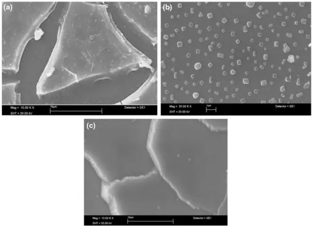
SEM images of the produced films are given in Fig. 2. The formation of large cracks or separation can be seen in the structure coated on ITO surface for which there are no peaks observed in the XRD pattern (Fig. 2a). Tiny crystal
particles at nano dimension could be observed on the struc-ture coated on the glass surface (Fig. 2b). The gaps between particles were too large and separated from each other. The fairly big crystal structure can be seen in Fig. 2c.
In the study, while the substrates are different, the coat-ing method is the same. The V5O9 and V8O15 oxide
lay-ers which are different forms of vanadium oxide on glass and Si wafer substrate are obtained. The different structural results may be the reason why vanadium oxide is physically coated on the amorphous glass, while attaching chemically on silicone at the oxygen part as seen in Fig. 3.
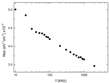
The capacitance–voltage–frequency (C–V–f) charac-teristics of the Al/VOx/p-Si/Al (MOS) structure were measured in the frequency range of 10 kHz–2 MHz and are given in Fig. 4, respectively. The measured C is strongly dependent on bias voltage and frequency. The accumulation capacitance decreases with increasing frequency. Such behavior of C is attributed to the par-ticular distribution of interface states (Nss) at VOx/p-Si
interfaces [21]. At low frequencies, Nss can easily
fol-low the ac signal and yield an excess capacitance, which depends on the frequency and time constant of interface states [22, 23]. However, in a sufficiently high frequency limit (f ≥ 500 kHz), the Nss can hardly follow the ac
sig-nal and contribution of the interface states capacitance to
Fig. 2 SEM images of VOx thin films at different substrates a ITO, b CG, c Si-wafer
~--• •~-•:S.:,\ (':0- J r'.••·{'(Y•rf'
the total capacitance may be neglected. The Nss obtained
from the slope of C−2–V plot as function frequency at
room temperature. As observed in Fig. 5 the values of
Nss decrease with increasing frequency and they become
almost constant at a high frequency. The high values of capacitance at low frequencies are attributed to the excess capacitance resulting from the Nss, which is in
equilibrium with the semiconductor that follows the ac signal. As could be seen in Fig. 5 and Table 1, the values of Nss are sufficiently low and promote the formation of a
low defect density interface. The obtained magnitudes of interface states of Al/VOx/p-Si (MOS) structure are suf-ficiently lower than Al/SnO2/p-Si and Al/SiO2/p-Si (MIS)
structures [15, 16].
Fig. 3 Coating mechanisms of VOx thin films
-2 -1 0 1 2 0.0 1.0x10⁻⁹ 2.0x10⁻⁹ 3.0x10⁻⁹ 4.0x10⁻⁹ 5.0x10⁻⁹ 6.0x10⁻⁹ Capacitance (F ) Voltage (V) 10 kHz 2 MHz
Fig. 4 The capacitance–voltage–frequency (C–V–f) characteristics of the Al/VOx/p-Si/Al (MOS) structure
10 100 1000 3.5 4.0 4.5 5.0 Nss (e V -1 cm -2 ) x1 0 12 f (kHz)
Fig. 5 Density of interface states (Nss) as a function of frequency
Table 1 The values of various parameters for Al/VOx/p-Si (MOS)
structure determined from C–V characteristics in the frequency range 10 kHz–2 MHz f (kHz) NA (1015cm−3) Vd (eV) WD (10−5 cm) NSS (1012 × eV−1 cm−2) 10 4.13 0.605 4.25 5.010 20 4.09 0.603 4.27 4.852 30 3.99 0.601 4.31 4.480 40 3.96 0.599 4.32 4.393 50 3.96 0.595 4.31 4.367 60 3.95 0.592 4.30 4.355 70 3.94 0.588 4.29 4.318 80 3.93 0.585 4.29 4.265 90 3.92 0.582 4.28 4.248 100 3.91 0.577 4.27 4.202 200 3.86 0.575 4.29 4.014 300 3.83 0.572 4.29 3.910 400 3.81 0.569 4.29 3.845 500 3.80 0.565 4.29 3.783 600 3.79 0.557 4.26 3.751 700 3.78 0.552 4.25 3.701 800 3.78 0.546 4.23 3.706 900 3.77 0.541 4.21 3.663 1000 3.76 0.533 4.18 3.645 2000 3.71 0.495 4.06 3.466
Physical absorption
AmorfGlassChemical absorption
(
i
0 0(
J:
r
Siliconr
•
•
•
•••
...
•
• •
••
....
•
4 Conclusion
In this study, we managed to produce the V8O15 derivative
of vanadium oxide, on glass, ITO and Si wafer substrates by wet chemical synthesis which is a simple and economi-cal method. While the structure of the film on ITO surface was observed to be amorphous from the XRD measure-ment results, the observed structure on glass sub-layer is V5O9 (PDF: 18-1450) in triclinic structure and the structure on Si substrate is V8O15 with three serial peaks with high magnitude despite slight deviation in angles. According to literature researches, it was observed that vanadium oxide thin films in V5O9 and V8O15 forms have not yet been pro-duced. In addition, Al/VOx/p-Si (MOS) electronic device structure was obtained from V8O15 structure. The interface
states of this structure were determined from the capaci-tance–voltage measurements depending on the frequency at room temperature. It was observed that the interface states values were dependent on the applied frequency. Besides, it was observed that the Nss values of Al/VOx/p-Si were
lower than those of MOS structures with SiO2 and SnO2. As a result, the electronic devices with V8O15 structure can be considered as an alternative to many oxidized MOS devices.
Acknowledgements This work is supported by Prime Ministry of Turkish, State Planning Organization (DPT) (Project Number: 2010K120610, Project Title: Batman University Central Research Laboratory).
References
1. G. Wu, J. Li, K. Wang, Y. Wang, C. Phan, A. Feng, J. Mater. Sci. doi:10.1007/s10854-017-6343-6
2. T.D. Manning, I.P. Parkini, Polyhedron 23, 3087 (2004)
3. G. Wu, Y. Cheng, Q. Xie, Z. Jia, F. Xiang, H. Wu, Mater. Lett. 144, 157 (2015)
4. X.J. Wang, H.D. Li, Y.J. Fei, X. Wang, Y.Y. Xiong, Y.X. Nieand, K.A. Feng, Appl. Surf. Sci. 177, 8 (2001)
5. G. Wu, Y. Ren, X. Li, L. Wang, Chemistry A 22(26), 8864 (2016)
6. S.H. Lee, H.M. Cheong, M.J. Seong, P. Liu, C.E. Tracy, A. Mas-carenhas, J.R. Pittsand, S.K. Deb, Solid State Ionics 165, 111 (2003)
7. G. Wu, Y. Cheng, F. Xiang, Z. Jia, Q. Xie, G. Wu, H. Wu, Mater. Sci. Semicond. Process. 41, 6 (2016)
8. G. Wu, Y. Cheng, Z. Wang, K. Wang, A. Feng, J. Mater. Sci. 28(1), 576 (2017)
9. G. Wu, Y. Wang, K. Wang, A. Feng, RSC Adv. 6(104), 102542 (2016)
10. G. Wang, H. Wu, K. Wang, C. Zheng, Y. Wang, A. Feng, RSC Adv. 6(63), 58069 (2016)
11. C.W. Park, S. Moon, H.B. Chung, J. Korean Phys. Soc. 39, 138 (2001)
12. G. Golan, A. Axelevitch, B. Sigalov, B. Gorenstein, Microelec-tron. J. 34, 255 (2003)
13. S. Chen, H. Ma, X. Yi, H. Wang, X. Tao, M. Chen, X. Liand C. Ke, Infrared Phys. Technol. 45, 239 (2004)
14. Z. Huang, H. Zeng, L. Xuea, X. Zhou, Y. Zhaoand, Q. Lai, J. Alloys Compd. 509, 10080 (2011)
15. K.J. Takeuchi, A.C. Marschilok, S.M. Davis, R.A. Leisingand E, S. Takeuchi, Coord. Chem. Rev. 219, 283 (2001)
16. R. T. R. Kumar, B. Karunagaran, D. Mangalaraj, S. K. Narayan-dass, P. Manoravi, M. Joseph, V. Gopal, Sens. Actuat. 107, 62 (2003)
17. F.J. Morin, Phys. Rev. Lett. 3, 34 (1959)
18. A. Tataroglu, Ş. Altındal, Microelectron. Eng. 83, 582 (2006) 19. O. Pakma, C. Tozlu, N. Kavasoglu, A.S. Kavasoglu, S. Özden, J.
Sol-Gel. Sci. Technol. 58, 244 (2011)
20. O. Pakma, N. Serin, T. Serin, J. Mater. Sci. 44, 401 (2009) 21. E.H. Nicollianand, J.R. Brews, Metal-oxide semiconductor
(MOS) physics and technology. (Wiley, New York, 1982)
22. S. Altındal, S. Karadeniz, N. Tugluoglu, A. Tataroglu, Solid State Electron. 47, 1847 (2003)