IOP PUBLISHING JOURNAL OF PHYSICS D: APPLIED PHYSICS
J. Phys. D: Appl. Phys. 45 (2012) 365102 (5pp) doi:10.1088/0022-3727/45/36/365102
Skin-like self-assembled monolayers on
InAs/GaSb superlattice photodetectors
Omer Salihoglu
1, Abdullah Muti
1, Kutlu Kutluer
2, Tunay Tansel
2,
Rasit Turan
2and Atilla Aydinli
11 Department of Physics, Bilkent University, 06800 Ankara, Turkey
2 Center for Solar Energy Research and Applications (GUNAM) and Department of Physics, Middle East¨ Technical University, 06531 Ankara, Turkey
1. Introduction
Infrared photodetectors based on type-II superlattice (T2SL) InAs/GaSb have recently attracted considerable interest due to the ability to engineer the band gap [1], suppression of Auger recombination [2] and low interband tunnelling [3]. Such advantages make type-II super lattice photodetector technology a promising alternative to mercury cadmium telluride (MCT) and quantum well infrared photodetectors (QWIPs) in focal plane array (FPA) applications. However, as the confinement of photocurrent typically requires the fabrication of a mesa structure, surface states due to dangling bonds, inversion layers and interfacial traps are generated due to the abrupt termination of the crystal structure on the mesa side walls, which mediate surface leakage currents. In order to overcome this, various passivation methods such as sulfide passivation [4], deposition of a dielectric layer [5,6], overgrowth with wide band gap materials [7], polymer film coatings, such as polyimide [8], have been proposed. Passivation is expected to suppress the oxidation of the side walls and saturate dangling bonds to prevent the formation of
for deposition or high RF powers to excite a plasma with potential for damage. Sulfur passivation replaces oxygen with sulfur and saturates the dangling bonds [10]. It is an effective passivation method and is easy to apply but the effect of passivation is temporary making it impractical [11]. It is usually applied using ammonium sulfide, sodium sulfide or zinc sulfide solutions. To increase the long-term stability of sulfur passivation, post-dielectric capping was used [12]. Alternatively, an electrochemical sulfur passivation (ECP) treatment was tried [4], but ECP does not prevent degradation with time, completely. Also, sulfur solutions etch GaSb layers (120nmmin−1) at 60◦C [13] resulting in porous layers damaging the superlattice structure. For InAs/GaSb SLs, with mesasetcheddowntotheGaSbbufferlayer,sulfurmayetchthe GaSb buffer introducing a series resistance, which may lead to asuperficialincreaseinthedynamicresistance,R0 [10]. Sulfur reduces the reverse bias dark current density by two orders of magnitude and increases the zero bias resistance (R0) by two orders of magnitude [4,5] while reducing photoresponsivity [10], which is masked by an increase in detectivity (D∗) due
2 E-mail: [email protected]
Received 16 May 2012, in final form 24 July 2012 Published 21 August 2012
Online at stacks.iop.org/JPhysD/45/365102 Abstract
We report on the effects of monolayer (ML) thick skin-like octadecanethiol (ODT, CH3[CH2]17SH) on type-II InAs/GaSb MWIR photodetectors. Circumventing the ageing effects of conventional sulfur compounds, we use ODT, a self-assembling, long molecular chain headed with a sulfur atom. Photodiodes coated with and without the self-assembled monolayer (SAM) ODT were compared for their electrical and optical performances. For ODT-coated diodes, the dark current density was improved by two orders of magnitude at 77K under −100mV bias. The zero bias responsivity and detectivity were 1.04AW−1 and
2.15 × 10¹³ Jones, respectively, at 4µm and 77K. The quantum efficiency was determined to be 37% for a cutoff wavelength of 5.1µm.
(Some figures may appear in colour only in the online journal)
assembled monolayer (SAM) octadecanethiol (ODT),
J. Phys. D: Appl. Phys. 45 (2012) 365102 O Salihoglu et al
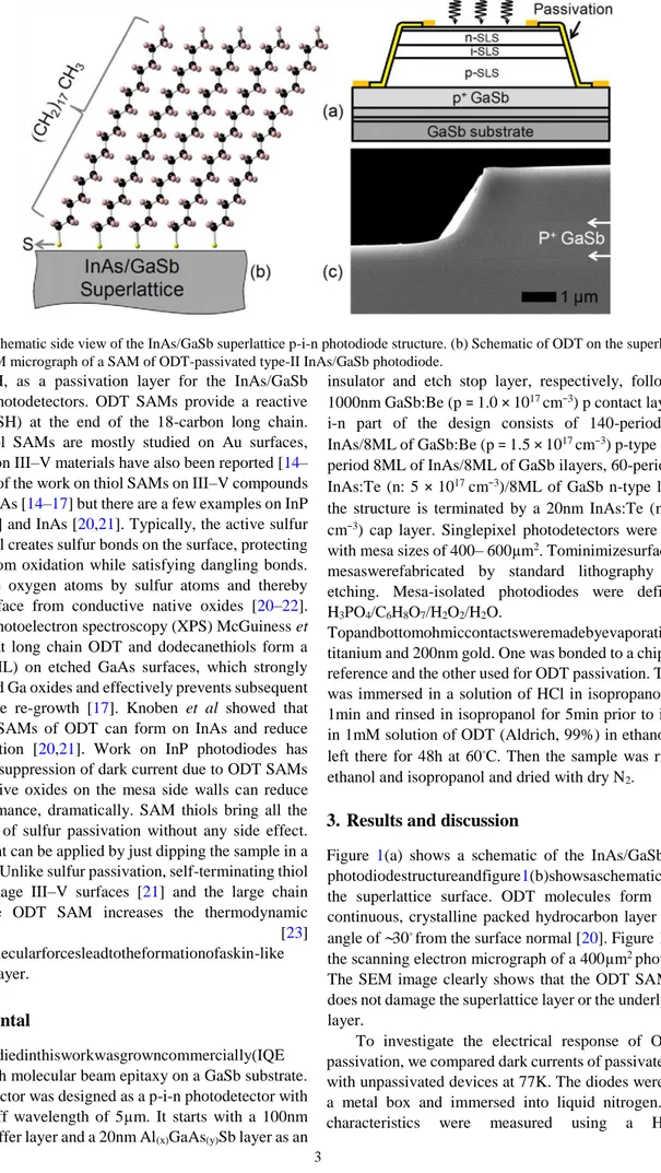
Figure 1. (a) Schematic side view of the InAs/GaSb superlattice p-i-n photodiode structure. (b) Schematic of ODT on the superlattice surface. (c) SEM micrograph of a SAM of ODT-passivated type-II InAs/GaSb photodiode.
CH3(CH2)17SH, as a passivation layer for the InAs/GaSb superlattice photodetectors. ODT SAMs provide a reactive sulfur head (SH) at the end of the 18-carbon long chain. Although thiol SAMs are mostly studied on Au surfaces, some studies on III–V materials have also been reported [14– 21]. Majority of the work on thiol SAMs on III–V compounds investigate GaAs [14–17] but there are a few examples on InP [18], GaP [19] and InAs [20,21]. Typically, the active sulfur end of the thiol creates sulfur bonds on the surface, protecting the surface from oxidation while satisfying dangling bonds. ODTs replace oxygen atoms by sulfur atoms and thereby clean the surface from conductive native oxides [20–22]. Using x-ray photoelectron spectroscopy (XPS) McGuiness et al showed that long chain ODT and dodecanethiols form a monolayer (ML) on etched GaAs surfaces, which strongly reduces As and Ga oxides and effectively prevents subsequent interface oxide re-growth [17]. Knoben et al showed that well-ordered SAMs of ODT can form on InAs and reduce surface oxidation [20,21]. Work on InP photodiodes has demonstrated suppression of dark current due to ODT SAMs [18]. Conductive oxides on the mesa side walls can reduce device performance, dramatically. SAM thiols bring all the good benefits of sulfur passivation without any side effect. Thiol treatment can be applied by just dipping the sample in a thiol solution. Unlike sulfur passivation, self-terminating thiol does not damage III–V surfaces [21] and the large chain length of the ODT SAM increases the thermodynamic
stability [23]
whereintermolecularforcesleadtotheformationofaskin-like hydrocarbon layer.
2. Experimental
Thesamplestudiedinthisworkwasgrowncommercially(IQE Inc. USA) with molecular beam epitaxy on a GaSb substrate. The photodetector was designed as a p-i-n photodetector with
insulator and etch stop layer, respectively, followed by a 1000nm GaSb:Be (p = 1.0 × 1017 cm−3) p contact layer. The p-i-n part of the design consists of 140-period 8ML of InAs/8ML of GaSb:Be (p = 1.5 × 1017 cm−3) p-type layers, 40-period 8ML of InAs/8ML of GaSb ilayers, 60-40-period 8ML of InAs:Te (n: 5 × 1017 cm−3)/8ML of GaSb n-type layers, and the structure is terminated by a 20nm InAs:Te (n: 5 × 1017 cm−3) cap layer. Singlepixel photodetectors were fabricated with mesa sizes of 400– 600µm2. Tominimizesurfacedamage, mesaswerefabricated by standard lithography and wet etching. Mesa-isolated photodiodes were defined with H3PO4/C6H8O7/H2O2/H2O.
Topandbottomohmiccontactsweremadebyevaporating5nm titanium and 200nm gold. One was bonded to a chip carrier as reference and the other used for ODT passivation. The sample was immersed in a solution of HCl in isopropanol (3M) for 1min and rinsed in isopropanol for 5min prior to immersion in 1mM solution of ODT (Aldrich, 99%) in ethanol and was left there for 48h at 60◦C. Then the sample was rinsed with ethanol and isopropanol and dried with dry N2.
3. Results and discussion
Figure 1(a) shows a schematic of the InAs/GaSb SL p-i-n photodiodestructureandfigure1(b)showsaschematicofODT on the superlattice surface. ODT molecules form a smooth, continuous, crystalline packed hydrocarbon layer with a tilt angle of ∼30◦ from the surface normal [20]. Figure 1(c) shows the scanning electron micrograph of a 400µm2 photodetector. The SEM image clearly shows that the ODT SAM solution does not damage the superlattice layer or the underlying GaSb layer.
To investigate the electrical response of ODT SAM passivation, we compared dark currents of passivated samples with unpassivated devices at 77K. The diodes were placed in
4 sourcemeasure unit. Figure 2(a) shows the measured dark current density versus applied bias voltage characteristics of the
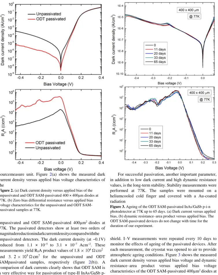
Figure 2. (a) Dark current density versus applied bias of the unpassivated and ODT SAM-passivated 400 × 400µm diodes at 77K. (b) Zero bias differential resistance versus applied bias voltage characteristics for the unpassivated and ODT SAM-passivated samples at 77K.
unpassivated and ODT SAM-passivated 400µm2 diodes at 77K. The passivated detectors show at least two orders of magnitudereductionindarkcurrentdensitycomparedwiththe unpassivated detectors. The dark current density (at −0.1V) reduced from 1.1 × 10⁻⁵ to 3.1 × 10⁻⁷ Acm−2. These measurements yield R0A product values of 1.
and 3. for the unpassivated and ODT SAMpassivated samples, respectively (figure 2(b)). A comparison of dark currents clearly shows that ODT SAM is a very effective way for passivation of type-II InAs/GaSb p-i-n photodetectors. The prominent reduction in dark current due to ODT SAM passivation is very encouraging when compared with the recently published type-II InAs/GaSb passivation works [11,24].
For successful passivation, another important parameter, in addition to low dark current and high dynamic resistance values, is the long-term stability. Stability measurements were performed at 77K. The samples were mounted on a heliumcooled cold finger and covered with a Au-coated radiation
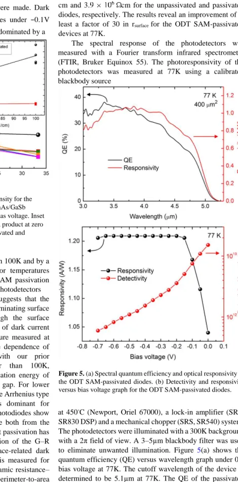
Figure 3. Ageing of the ODT SAM-passivated InAs/GaSb p-i-n photodetector at 77K up to 65 days. (a) Dark current versus applied bias, (b) dynamic resistance–area product versus applied bias. The ODT SAM-passivated devices do not change with time for the duration of our experiment.
shield. I–V measurements were repeated every 10 days to monitor the effects of ageing of the passivated devices. After each measurement, the cryostat was opened to air to provide atmospheric ageing conditions. Figure 3 shows the measured dark current density versus applied bias voltage and dynamic resistance–area product versus applied bias voltage characteristics of the ODT SAM-passivated 400µm2 diodes at 77Kwithatleastaten-dayintervalbetweenthemeasurements. Dark current measurements indicate that the ODT SAM does not show any sign of ageing even after 65 days. Strong intermolecular interactions between the long chains of ODT molecules form a closely packed and thermodynamically
J. Phys. D: Appl. Phys. 45 (2012) 365102 O Salihoglu et al
stable skin-like layer. This reinforced sulfurization method is expected to form an inert surface. Small fluctuations are due to the noise floor of our instrument.
To understand the nature of the dark current, temperaturedependent I–V measurements were made. Dark current densities versus inverse temperatures under −0.1V bias are shown in figure 4. The I–V curve is dominated by a
Figure 4. Temperature-dependent dark current density for the unpassivated and ODT SAM-passivated type-II InAs/GaSb superlattice 400 × 400µm photodiodes at −0.1V bias voltage. Inset shows the dependence of dynamic resistance–area product at zero bias versus perimeter-to-area ratio for the unpassivated and passivated devices at 77K.
diffusion current for temperatures higher than 100K and by a generation–recombination (G–R) current for temperatures lower than 100K. The diodes with ODT SAM passivation showalowerdarkcurrentthantheunpassivatedphotodetectors for temperatures lower than 100K. This suggests that the passivation process reduces native oxides eliminating surface states and preventing current flow through the surface channel. Figure 4 also shows the summary of dark current density at −0.1V as a function of temperature measured at different stages of ageing. The temperature dependence of ageing over 60 days is consistent with our prior measurements. For temperatures higher than 100K, Arrhenius-type behaviour yielded an activation energy of 0.23eV, which is close to the device band gap. For lower temperatures, current begins to divert from the Arrhenius type of behaviour. The G–R current becomes dominant for temperatures below 100K. The passivated photodiodes show reduced G–R currents, which may originate both from the bulk and the surface. Our results indicate that passivation has led to a reduction in the surface contribution of the G–R current. Alternatively, to analyse the surface-related dark current behaviour, the dynamic resistance is measured for different mesa sizes. The inverse of the dynamic resistance– area product at zero bias as a function of the perimeter-to-area
ratio at 77K for the passivated and unpassivated detectors is shown in the inset of figure 4. The surface resistance can be calculated from the slope of the graph [24]. The calculated surface resistivity (rsurface) values at zero bias are 1.
cm and 3. cm for the unpassivated and passivated diodes, respectively. The results reveal an improvement of at least a factor of 30 in rsurface for the ODT SAM-passivated devices at 77K.
The spectral response of the photodetectors was measured with a Fourier transform infrared spectrometer (FTIR, Bruker Equinox 55). The photoresponsivity of the photodetectors was measured at 77K using a calibrated blackbody source
Figure 5. (a) Spectral quantum efficiency and optical responsivity of the ODT SAM-passivated diodes. (b) Detectivity and responsivity versus bias voltage graph for the ODT SAM-passivated diodes.
at 450◦C (Newport, Oriel 67000), a lock-in amplifier (SRS, SR830 DSP) and a mechanical chopper (SRS, SR540) system. The photodetectors were illuminated with a 300K background with a 2π field of view. A 3–5µm blackbody filter was used to eliminate unwanted illumination. Figure 5(a) shows the quantum efficiency (QE) versus wavelength graph under 0V bias voltage at 77K. The cutoff wavelength of the device is determined to be 5.1µm at 77K. The QE of the passivated
6 photodetector is determined as high as 37% for these single pass detectors under front illumination around 3.5µm wavelength. Since the QE is directly related to the thickness of the absorbing layer, it is difficult to make direct comparisons with other published data due to differences betweenstructures. Inanycase, 37%QEinourphotodetectors is high among type-II InAs/GaSb superlattice papers [25,26]. Figure 5(b) shows the responsivity and Johnson-noiselimited detectivity (D∗) versus applied bias voltage graph for the ODT SAM-passivated photodetector. The zero bias responsivity of the ODT-passivated photodetector was equal to 1.04AW−1 at 4µm and 77K. Under zero bias, the peak D∗ was found to be 2.15 × 10¹³ Jones for the passivated photodetector at 4µm and 77K. When we compare our results with recently published type-II InAs/GaSb passivation works [11,24], the ODT-passivated T2SL photodetectors are very promising.
The influence of the ODT SAM on the performance of the T2SL is closely related to the surface chemistry of the superlattice. Chemically reactive InAs/GaSb SL surfaces are easily oxidized and a native oxide layer of several nanometres thick is quickly formed upon exposure to air. These form conductive channels and lead to surface leakage. However, sulfur is chemically preferred over oxygen, and replaces oxygen to form surface sulfides that are electrically less active. The interaction of sulfur with InAs creates InxSy and
AsxSy (InAs + 2HS and the
interactionwithGaSbcreatesGaxSy andSbxSy (GaSb+2HS =
Ga on the surface. These may be called
interfacial self-cleaning reactions of surface oxides with sulfur as determined by XPS measurements [17,21]. Finally, strong intermolecular interactions between long chains of ODT molecules form a closely packed and thermodynamically stableskin-likeultrathinprotectivelayer. Theseresultssuggest that this process is beneficial for FPA and LWIR applications.
4. Conclusions
We have demonstrated the suppression of dark current and increase in optical response of InAs/GaSb superlattice photodetectors with cutoff wavelength at 5.1µm (MWIR). We have used ODT SAM passivation of InAs/GaSb p-in superlattice photodetectors. The passivated superlattice photodetectors reduced the dark current from 1.1 × 10⁻⁵ to 3.1 × 10⁻⁷ Acm−2 compared with the unpassivated photodetectorat77Kandunder−0.1Vappliedbiascondition. The corresponding zero bias–area product (R0A) is improved bytwoordersofmagnitude(from1.
The zero bias responsivity and detectivity (D∗) are determined to be 1.04AW−1 and 2.15 × 10¹³ Jones, respectively at 4µm and 77K. The quantum efficiency (QE) of the passivated photodetector is determined to be 37% under the single pass front illumination condition. Temperature-dependent dark current and dynamic resistance–area product as a function of
the perimeter-to-area ratio measurements revealed that passivation prevents photodetectors from being dominated by surface currents for temperatures below 100K. The devices show Arrhenius type of behaviour at higher temperatures, an indication that the dominant current is the bulk diffusion currentforhightemperatures. Thecalculatedactivationenergy is equal to 0.23eV, which is close to the device band gap. The dark current performance of the photodiodes did not degrade for 65 days after the passivation, indicating long-term stability.
ThisworkshowsthatODTSAMisagoodpassivationmaterial for p-i-n InAs/GaSb superlattice photodetectors.
References
[1] Wei Y J and Razeghi M 2004 Phys. Rev. B 69 085316 [2] Grein C H, Young P M and Ehrenreich H 1992 Appl. Phys. Lett. 61 2905–7
[3] Smith D L and Mailhiot C 1987 J. Appl. Phys. 62 2545–8 [4] Plis E, Rodriguez J B, Lee S J and Krishna S 2006 Electron. Lett. 42 1248–9
[5] Gin A, Wei Y J, Bae J J, Hood A, Nah J and Razeghi M 2004 Thin Solid Films 447 489–92
[6] Salihoglu O, Muti A, Kutluer K, Tansel T, Turan R and Aydinli A 2012 J. Appl. Phys. 111 074509
[7] Rehm R, Walther M, Fuchs F, Schmitz J and Fleissner J 2005 Appl. Phys. Lett. 86 173501
[8] Hood A, Delaunay P Y, Hoffman D, Nguyen B M, Wei Y J, Razeghi M and Nathan V 2007 Appl. Phys. Lett. 90 233513
[9] Tansel T, Kutluer K, Salihoglu O, Aydinli A, Aslan B, Arikan B, Kilinc M C, Ergun Y, Serincan U and Turan R 2012 IEEE Photon. Technol. Lett. 24 790–2
[10] Hoffmann J, Lehnert T, Hoffmann D and Fouckhardt H 2009 Semicond. Sci. Technol. 24 065008
[11] Plis E, Kutty M N, Myers S, Kim H S, Gautam N, Dawson L R and Krishna S 2011 Infrared Phys. Technol. 54 252–7 [12] Li J V, Chuang S L, Sulima O V and Cox J A 2005 J. Appl.
Phys. 97 104506
[13] Hood A, Wei Y, Gin A, Razeghi M, Tidrow M Z and Nathan V 2005 Proc. SPIE 5732 316–25
[14] Ye S, Li G F, Noda H, Uosaki K and Osawa M 2003 Surf. Sci.
529 163–70
[15] Jun Y, Zhu X Y and Hsu J W P 2006 Langmuir 22 3627–32 [16] Budz H A and LaPierre R R 2008 J. Vac. Sci. Technol. A
26 1425–31
[17] McGuiness C L, Shaporenko A, Zharnikov M, Walker A V and Allara D L 2007 J. Phys. Chem. C 111 4226–34 [18] Schvartzman M, Sidorov V, Ritter D and Paz Y 2003 J. Vac.
Sci. Technol. B 21 148–55
[19] Flores-Perez R, Zemlyanov D Y and Ivanisevic A 2008 Surf. Sci. 602 1993–8
[20] Knoben W, Brongersma S H and Crego-Calama M 2009 J. Phys. Chem. C 113 18331–40
[21] Petrovykh D Y, Smith J C, Clark T D, Stine R, Baker L A and Whitman L J 2009 Langmuir 25 12185–94 [22] Spindt C J, Liu D, Miyano K, Meissner P L, Chiang T T, Kendelewicz T, Lindau I and Spicer W E 1989 Appl. Phys.
J. Phys. D: Appl. Phys. 45 (2012) 365102 O Salihoglu et al
Lett. 55 861–3
[23] Love J C, Estroff L A, Kriebel J K, Nuzzo R G and Whitesides G M 2005 Chem. Rev. 105 1103–69 [24] Kim H S, Plis E, Khoshakhlagh A, Myers S, Gautam N,
Sharma Y D, Dawson L R, Krishna S, Lee S J and Noh S K
2010 Appl. Phys. Lett. 96 033502
[25] Kim H S et al 2008 Appl. Phys. Lett. 92 183502
[26] Chen G, Nguyen B M, Hoang A M, Huang E K, Darvish S R and Razeghi M 2011 Appl. Phys. Lett. 99 183503