Highly directional enhanced radiation
from sources embedded inside
three-dimensional photonic crystals
Humeyra Caglayan, Irfan Bulu, and Ekmel Ozbay
Department of Physics and the Nanotechnology Research Center, Bilkent University, 06800 Ankara, Turkey
Abstract:
We have experimentally studied emission of microwave radiation from a monopole source embedded in a three-dimensional photonic crystal. We have demonstrated enhancement of microwave radiation at the band edge and cavity mode frequencies. Furthermore, we have shown that it is possible to obtain highly directive microwave radiation sources operating at the band edge of the three-dimensional photonic crystal. We have measured half power beam widths of 13ofor both E and H planes, corresponding to a maximum directivity of 245.
© 2005 Optical Society of America
OCIS codes: (999.9999) Photonic crystal, (999.9999) Enhanced radiation
References and links
1. S. John, “Strong localization of photons in certain disordered dielectric superlattices,” Phys. Rev. Lett. 58, 2486 (1987).
2. E. Yablonovitch,“Inhibited Spontaneous Emission in Solid-State Physics and Electronics,” Phys. Rev. Lett. 58, 2059 (1987).
3. J. D. Joannopoulos, R. D. Meade, and J. N. Winn, Photonic Crystal: Molding the Flow of Light (Princeton University Press, Princeton, NJ, 1995.).
4. O. Painter, R. K. Lee, A. Scherer, A. Yariv, J. D. O’Brien, P. D. Dapkus, and I. Kim, “Optical Properties of an Ionic-Type Phononic Crystal,” Science 284, 1819 (1999).
5. B. Temelkuran, M. Bayindir, E. Ozbay, R. Biswas, M. M. Sigalas, G. Tuttle, and K. M. Ho, “Photonic crystal-based resonant antenna with a very high directivity,” J. Appl. Phys. 87, 603 (2000).
6. K. Busch and S. John, “Liquid-Crystal Photonic-Band-Gap Materials: The Tunable Electromagnetic Vacuum,” Phys. Rev. Lett. 83, 967 (1999).
7. F. De Martini, M. Marrocco, P. Mataloni, and D. Murra, “Spontaneous and stimulated emission in the threshold-less microlaser,” J. Opt. Soc. Am. B 10, 360 (1993).
8. P. R. Villenevue, S. Fan, J. D.Joannopoulos, K. Y. Lim, G. S. Petrich, L. A. Kolodjeski, and R. Reif, “Air-bridge microcavities,” Appl. Phys. Lett. 67, 167 (1995).
9. P. L. Gourley, J. R.Wendt, G. A. Vawter, T. M. Brennan, and B. E. Hammons, “Optical properties of two-dimensional photonic lattices fabricated as honeycomb nanostructures in compound semiconductors,” Appl. Phys. Lett. 64, 687 (1994).
10. J. P. Dowling, M. Scalora, M. J. Bloemer, and C. M. Bowden, “The photonic band edge laser: A new approach to gain enhancement,” J. Appl. Phys. 75, 1896 (1994).
11. E. R. Brown, C. D. Parker, and E. Yablonovitch, “Radiation properties of a planar antenna on a photonic-crystal substrate,” J. Opt. Soc. Am. B 10, 404 (1993).
12. K. Busch, N. Vats, S. John, and B. C. Sanders, “Radiating dipoles in photonic crystals,” Phys. Rev. E 62, 4251-4260 (2000).
13. V. Lousse, J. Vigneron, X. Bouju, and J. Vigoureux, “Atomic radiation rates in photonic crystals,” Phys. Rev. B 64, 201104 (2001).
14. A. Asatryan, K. Busch, R. C. McPhedran, L. C. Botten, C. Martijn de Sterke, and N. A. Nicorovici, “Two-dimensional Green’s function and local density of states in photonic crystals consisting of a finite number of cylinders of infinite length,” Phys. Rev. E 63, 046612 (2001).
15. S. John and T. Quang, “Spontaneous emission near the edge of a photonic band gap,” Phys. Rev. A 50, 1764-1769 (1994).
16. D. N. Chigrin, “Radiation pattern of a classical dipole in a photonic crystal: Photon focusing,” Phys. Rev. E 70, 056611 (2004).
17. B. Taylor, H. J. Maris, and C. Elbaum, “Phonon Focusing in Solids ,” Phys. Rev. Lett. 23, 416 (1969).
18. E. R. Brown and O. B. McMahon, “High zenithal directivity from a dipole antenna on a photonic crystal ,” Appl. Phys. Lett. 68, 1300 (1996).
19. R. Gonzalo, P. de Maagt, and M. Sorolla, “Enhanced patch-antenna performance by suppressing surface waves using photonic-bandgap substrates,” IEEE Trans. Microwave Theory Tech. 47 (11), 2131 (1999).
20. I. Bulu, H. Caglayan, and E. Ozbay, “Highly directive radiation from sources embedded inside photonic crystals,” Appl. Phys. Lett. 83, 3263 (2003).
21. I. Bulu, H. Caglayan, and E. Ozbay, “Radiation properties of sources inside photonic crystals,” Phys. Rev. B 67, 205103 (2003).
22. M. Bayindir and E. Ozbay, “Heavy photons at coupled-cavity waveguide band edges in a three-dimensional photonic crystal ,” Phys. Rev. B 62, R2247-R2250 (2000).
23. S. Yano, Y. Segawa, J. S. Bae, K. Mizuno, S. Yamaguchi, and K. Ohtaka, “Optical properties of monolayer lattice and three-dimensional photonic crystals using dielectric spheres,” Phys. Rev. B 66, 075119 (2002).
24. T. Kondo, M. Hangyo, S. Yamaguchi, S. Yano, Y. Segawa, and K. Ohtaka, “Transmission characteristics of a two-dimensional photonic crystal array of dielectric spheres using subterahertz time domain spectroscopy,” Phys. Rev. B 66, 033111 (2002).
25. K. Ohtaka, Y. Suda, S. Nagano, T. Ueta, A. Imada, T. Koda, J. S. Bae, K. Mizuno, S. Yano, and Y. Segawa, “Photonic band effects in a two-dimensional array of dielectric spheres in the millimeter-wave region,” Phys. Rev. B 61, 5267 (2000).
26. K. Ohtaka, J. Inoue, and S. Yamaguti, “ Derivation of the density of states of leaky photonic bands,” Phys. Rev. B 70, 035109 (2004).
27. K. Sakoda, Optical Properties of Photonic Crystals (Springer-Verlag, Germany, 2001).
28. K. Sakoda and K. Ohtaka, “Optical response of three-dimensional photonic lattices: Solutions of inhomogeneous Maxwell’s equations and their applications,” Phys. Rev. B 54, 5732 (1996).
29. M. Wubs and A. Lagendijk, “Local optical density of states in finite crystals of plane scatterers ,” Phys. Rev. E 65, 046612 (2002).
30. E. Ozbay, “Layer-by-layer photonic crystals from microwave to far-infrared frequencies,” J. Opt. Soc. Am. B 13, 1945 (1996).
31. K. M. Ho, C. T. Chan, C. M. Soukoulis, R. Biswas, and M. Sigalas, “Photonic band gaps in three dimensions: New layer-by-layer periodic structures,” Solid State Commun. 89, 413 (1994).
32. E. Ozbay, A. Abeyta, G. Tuttle, M. Tringides, R. Biswas,C. T. Chan, C. M. Soukoulis, and K. M. Ho, “Measure-ment of a three-dimensional photonic band gap in a crystal structure made of dielectric rods ,” Phys. Rev. B 50, 1945 (1994).
33. S.Noda, K.Tomoda, N.Yamamoto, and A. Chutinan, “Full Three-Dimensional Photonic Bandgap Crystals at Near-Infrared Wavelengths,” Science, 289, 604 (2000).
34. S. Ogawa, M. Imada, S. Yoshimoto, M. Okano, and S. Noda, Control of Light Emission by 3D Photonic Crystals,” Science 305, 227 (2004).
35. S. Noda, M. Imada, M. Okano, S. Ogawa, M. Mochizuki, and A. Chutinan, “Semiconductor three-dimensional and two-dimensional photonic crystals and devices,” IEEE J.Quantum Electron. 38(7), 726 (2002).
36. M. Okano, A. Chutinan, and S. Noda, “Analysis and design of single-defect cavities in a three-dimensional photonic crystal,” Phys. Rev. B 66, 165211 (2002).
37. E. Ozbay, G. Tuttle, M. Sigalas, C. M. Soukoulis and K. M. Ho, “Defect structures in a layer-by-layer photonic band-gap crystal,” Phys. Rev. B 51, 13961 (1995).
38. B. Temelkuran, E. Ozbay, J. P. Kavanaugh, G. Tuttle, and K. M. Ho, “Resonant cavity enhanced detectors em-bedded in photonic crystals,” Appl. Phys. Lett. 72, 2376 (1998).
39. M. M. Sigalas, R. Biswas, K. M. Ho, C. M. Soukoulis, D. Turner, B. Vasiliu, S. C. Kothari, and S. Lin, “Waveguide bends in three-dimensional layer-by-layer photonic bandgap materials,” Micro. Opt. Tech. Lett., 23, 56 (1999).
40. H. Park, J.Hwang, J. Huh, H. Ryu, S. Kim, J. Kim, and Y.Lee, “Characteristics of modified single-defect two-dimensional photonic crystal lasers,” IEEE J.Quantum Electron. 38 (10), 1353 (2002).
41. M. Agio, E. Lidorikis, and C. M. Soukoulis, “Impurity modes in a two-dimensional photonic crystal: coupling efficiency and Q factor ,” J. Opt. Soc. Am. B 17 (12), 2037 (2000).
42. S. Enoch, B. Gralak, and G. Tayeb, “Enhanced emission with angular confinement from photonic crystals,” App. Phys. Lett. 81 (9), 1588 (2002).
0 5 10 15
K'
W
X'
Γ
Frequency (GHz)
X' K
L
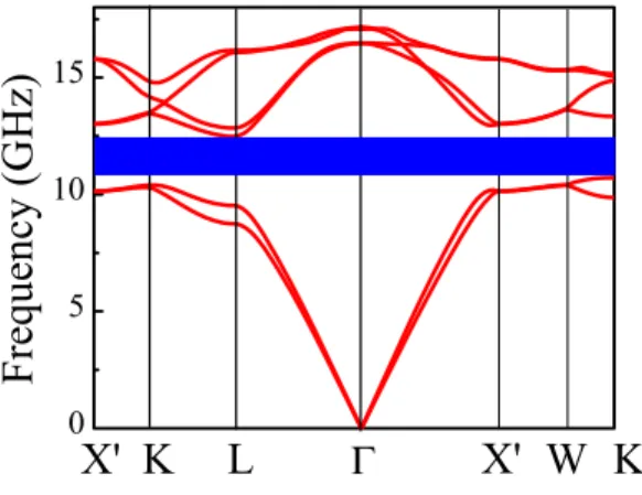
Fig. 1. Band diagram for the 3D layer-by-layer dielectric photonic crystal.
Photonic crystals (PCs) are structures with periodic dielectric constant variations, in which electromagnetic (EM) wave propagation is forbidden in all directions for a certain range of frequencies [1, 2]. These electromagnetic band gaps can be used for a wide range of applica-tions [3], such as microscopic lasers [4], resonant antennas [5] and optical switches [6]. Among these applications, there is a great deal of growing interest to use PCs to control the spontaneous emission in photonic devices leading to more efficient light emitters such as thresholdless semi-conductor lasers [7, 8], single-mode light-emitting diodes [9, 10] and efficient antennas [11].
Previously, several researchers theoretically investigated the effect of PCs on the radiation properties of sources embedded inside PCs [12, 13]. It has been shown that PCs strongly mod-ify the emission properties of sources. This strong modification is due to the strong modifica-tion of the radiative local density of states. Theoretical works on atomic radiamodifica-tions from dipolar sources embedded inside PCs have predicted several interesting phenomena, such as enhance-ment or suppression of radiation [13, 14], photon-source bound states [15]. In addition, it has been shown that PCs modify the angular distribution of power from radiation sources due to the strong dispersion and anisotropy [16]. At a distant observation point, the main contribu-tion the electromagnetic fields come from the modes whose group velocity direccontribu-tion coincides with the direction to the observation point. This effect is similar to the ”phonon focusing” that was observed by Taylor et al. [17] in crystalline solids for the phonon field. In spite of these numerous theoretical works there are a few experimental works investigating the effect of PCs on the radiation properties of sources. The lack of experimental work is due to difficulties in preparation of samples, especially in difficulties preparing 3 dimensional (3D) PCs that operate in the optical region. Busch et al. [12] have shown that PCs modify the emission properties of sources in the microwave region and in the optical region in the same manner. In this sense, the investigation of the effect of PCs on the radiation properties of sources in the microwave region is important and may provide further insight.
The photonic band gap edges are especially important for the study of the effect of PCs on the radiation properties of sources. The importance of the band edge lies in the fact that radiative local density of states is strongly enhanced near the band edge frequencies [13]. The radiative local density of states is a measure of the coupling of the source to the electromagnetic modes of the photonic crystal structure. It depends on group velocity of the eigen-modes of the
Fig. 2. Schematics of 3D layer-by-layer photonic crystal.
PC, the orientation of the dipole moment of the source, and the overlap between the electric field of the modes of the PC and the dipole moment of the source. In addition, near the band edge frequencies the directions of the allowed wave vectors are confined to the close vicinity of a certain direction. The allowed wave vectors for a certain frequency constitute a surface in the three dimensional Brillouin zone i.e, equal frequency surface (EFS). At the band edge frequency the EFS shrinks to the close vicinity of a certain point. This limits the directions of the allowed wave vectors to a certain preferred direction.
The reported experimental and theoretical studies on PC based antenna applications mostly used total reflection property of these structures. The antennas mounted on PC substrate sur-faces exhibited high efficiency and directivity compared to conventional antennas on dielec-tric substrates [18, 19]. In all of these works, the radiation sources were placed outside of the sources. But, PCs can also be used to improve the directivity of the sources, by embedding these sources inside the PCs [20]. In this sense, PCs can be used in the solution of two main problems of the control of emission: enhancement of radiation and confinement of the emitted power to a narrow angular region [20, 21].
In our previous works [20, 21], we have studied emission of radiation from a source embed-ded in two-dimensional (2D) PC. We demonstrated the enhancement of radiation and confine-ment of radiation to a very narrow angular region using a 2D PC. In addition to enhanceconfine-ment of radiation, we showed that emitted power can be confined to a narrow angular region. We obtained half power beam widths as small as 6o. Although we obtained angular confinement by using a 2D PC, the confinement is only in 2 dimension. In order to achieve angular confinement in 3 dimension one have to use 3D PCs.
In this paper, we have studied emission of radiation from a monopole source embedded inside a 3D PC in order to get an enhancement of radiation and to confine emitted power to a narrow angular region in two planes (E and H planes). We have demonstrated the enhancement of radiation at the band edge and at the cavity mode frequencies. Moreover, we have shown that it is possible to confine the emitted power to a narrow angular region in 3 dimensions.
The monopole antenna that we used in our experiments is constructed by removing the shield around one end of a microwave coaxial cable. The cleaved center conductor, which also acted as the radiation source, is 5 mm long. An HP-8510C network analyzer is used to excite the monopole source and a standard gain horn antenna is used to receive the radiated EM field from the monopole antenna. The HP-8510C network analyzer is capable of measuring both intensity
10.0 10.2 10.4 -30 -20 -10 0 0 5 10 15
Transm
is
si
on (
dB)
Frequency (GHz) Dela y time ( ns ) 10 12 14 16 -60 -40 -20 0 Experiment Transmission ( dB ) Frequency (GHz) FDTD Simulation(a)
(b)
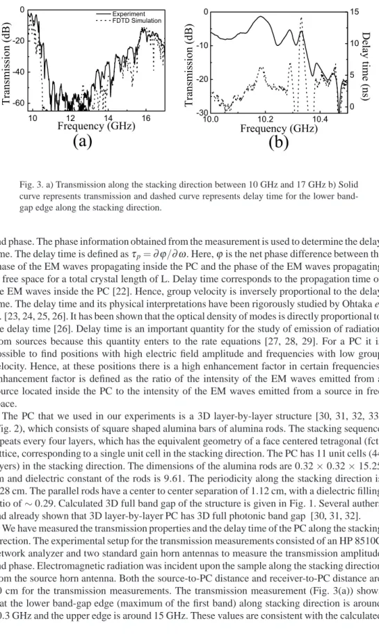
Fig. 3. a) Transmission along the stacking direction between 10 GHz and 17 GHz b) Solid curve represents transmission and dashed curve represents delay time for the lower band-gap edge along the stacking direction.
and phase. The phase information obtained from the measurement is used to determine the delay time. The delay time is defined asτp=∂ϕ/∂ω. Here,ϕis the net phase difference between the phase of the EM waves propagating inside the PC and the phase of the EM waves propagating in free space for a total crystal length of L. Delay time corresponds to the propagation time of the EM waves inside the PC [22]. Hence, group velocity is inversely proportional to the delay time. The delay time and its physical interpretations have been rigorously studied by Ohtaka et al. [23, 24, 25, 26]. It has been shown that the optical density of modes is directly proportional to the delay time [26]. Delay time is an important quantity for the study of emission of radiation from sources because this quantity enters to the rate equations [27, 28, 29]. For a PC it is possible to find positions with high electric field amplitude and frequencies with low group velocity. Hence, at these positions there is a high enhancement factor in certain frequencies. Enhancement factor is defined as the ratio of the intensity of the EM waves emitted from a source located inside the PC to the intensity of the EM waves emitted from a source in free space.
The PC that we used in our experiments is a 3D layer-by-layer structure [30, 31, 32, 33] (Fig. 2), which consists of square shaped alumina bars of alumina rods. The stacking sequence repeats every four layers, which has the equivalent geometry of a face centered tetragonal (fct) lattice, corresponding to a single unit cell in the stacking direction. The PC has 11 unit cells (44 layers) in the stacking direction. The dimensions of the alumina rods are 0.32 × 0.32 × 15.25 cm and dielectric constant of the rods is 9.61. The periodicity along the stacking direction is
1.28 cm. The parallel rods have a center to center separation of 1.12 cm, with a dielectric filling
ratio of∼ 0.29. Calculated 3D full band gap of the structure is given in Fig. 1. Several authers had already shown that 3D layer-by-layer PC has 3D full photonic band gap [30, 31, 32].
We have measured the transmission properties and the delay time of the PC along the stacking direction. The experimental setup for the transmission measurements consisted of an HP 8510C network analyzer and two standard gain horn antennas to measure the transmission amplitude and phase. Electromagnetic radiation was incident upon the sample along the stacking direction from the source horn antenna. Both the source-to-PC distance and receiver-to-PC distance are 10 cm for the transmission measurements. The transmission measurement (Fig. 3(a)) shows that the lower band-gap edge (maximum of the first band) along stacking direction is around
10.00 10.2 10.4 5 10 15
Enhancement
Factor
Frequency (GHz)
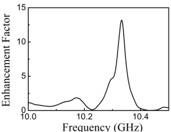
Fig. 4. Enhancement factor around the lower band-gap edge along the stacking direction.
11.4 11.7 12.0 12.3 12.6 0.0 0.2 0.4 0.6 0.8 1.0 Experiment FDTD Simulation
Tr
ansm
ission (
10
-3)
Frequency (GHz)
12.00 12.02 12.04 12.06 12.08 0.0 0.2 0.4 0.6 0.8 1.0 0 20 40Tr
ansm
ission (10
-3)
Frequency (GHz)
Del
ay ti
me (
ns
)
(a)
(b)
Fig. 5. a) Calculated and measured transmission of the cavity mode along the stacking direction. b) Solid curve represents transmission and dashed curve represents delay time for the cavity mode.
photonic band structure (Fig. 1). The measured delay times around the lower band-gap edge are presented in Fig. 3(b). The delay time near the lower edge is 14.2 nsec. The time required for the EM waves to propagate along the structure which is 0.47 nsec. So, the PC reduces the group velocity of light at this frequency by a factor of 30.
The enhancement factor for the EM waves emitted from a monopole source along the stack-ing direction is measured. The monopole source is located at the center of the PC, between the 21st and 22nd layer in the 6th unit cell of the PC. Figure 4 shows the enhancement factor for frequencies near the lower edge. A maximum enhancement factor of 13.7 is obtained at 10.3 GHz, which also corresponds to the lower band-gap edge frequency.
Single cavity structures are very important features for the control of emission from radia-tion sources. Recently, Noda group [34] fabricated (3D) PCs containing artificial point defects to emit light at optical communications wavelengths. The properties of a single-defect cavity investigated [35, 36, 37] and resonant cavity enhanced detectors [38] and waveguide
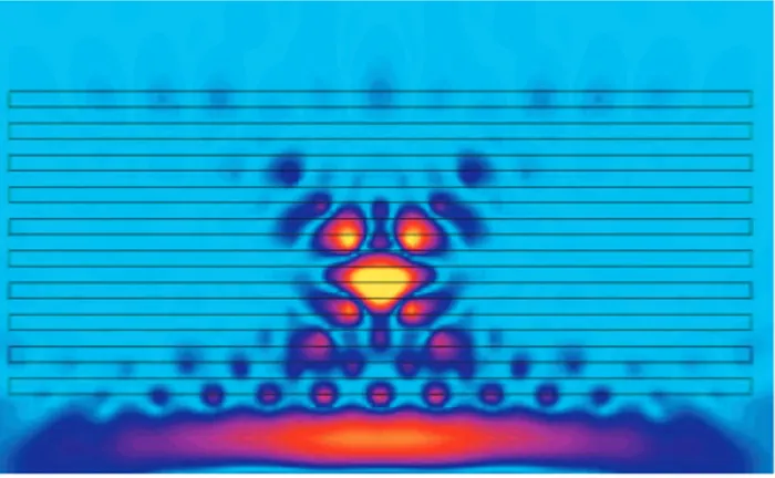
applica-Fig. 6. FDTD calculation of electric-field intensity for the cavity mode. The missing rod is at the center of the structure.
11.9 12.0 12.1 12.2 0 5 10 15 20
Enhancement Factor
Frequency (GHz)
Fig. 7. Enhancement factor for a monopole source located inside a cavity.
tions [39] were demonstrated using localized modes of the cavities built in PCs. In order to obtain a single cavity localized in the PC, we have removed the center rod of a 20-layer 3D PC. The measured transmission and delay time for the single cavity structure are shown in Fig. 5. The defect mode is at 12.04 GHz with a Q-factor (quality factor, defined as the center fre-quency divided by the full width at half maximum) of 1430. The delay time at the defect mode frequency is 47 nsec. This also means that at the defect mode the group velocity is reduced by a factor of 220 when compared to the electromagnetic waves propagating in free space. Electric-field intensity of the cavity mode is highly localized at the center of the cavity (Fig 6). Q-factor, group velocity reduction factor and enhancement factor are related through the localization of EM waves. It is also important to note that, the delay time is directly proportional to the quality factor viaτp∝Q/ω[22, 40, 41]. The measured enhancement factor for the EM waves emitted from a monopole source embedded inside the cavity is shown in Fig 7. The enhancement factor is around 20 at 12.07 GHz. Compared to the enhancement factor that we obtained in 2D sys-tem [21], our 3D cavity exhibits 4 times larger enhancement factor. Our results show that 3D PCs can be used to enhance the emitted power from a monopole source.
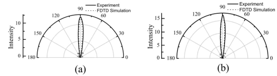
0 30 60 90 120 150 180 Experiment FDTD Simulation Inte nsi ty 0 5 10 15 0 30 60 90 120 150 180 Experiment FDTD Simulation Intensity 0 5 10
(a)
(b)
Fig. 8. The measured and calculated radiation patterns of the monopole antenna inside the 3D photonic crystal for a)E and b)H planes.
The modes at the band edges of a PC are propagating modes and these modes are concen-trated in low or high dielectric material region. Hence, the surface of the PC can be regarded as a system of radiation sources all operating at the band edge frequency, having similar spatial and temporal distribution of power with a uniform phase difference between the radiators [21]. This system of radiators is similar to an array of antennas. Since all the radiators of the system radiate inΓ− S direction, we expect the emitted power from a source embedded inside the PC to be confined to a narrow angular region [42]. Due to the 3D band gap, the angular confinement is also in 3 dimensions.
We have measured the angular distribution of power at the lower band-gap edge frequency, 10.3 GHz, for E and H planes [43]. For antennas with one narrow major lobe and very negligible minor lobes in the radiation pattern, the maximum directivity is given as [43]
D0∼=
4π
Θ1Θ2
(1) whereΘ1is half power beam width of one plane (E-plane) andΘ2is the perpendicular plane
to the first (H-plane), in radians. The measured half power beam widths along the E- plane and H-plane are presented in Fig. 8. In Fig. 8, 90ocorresponds to the stacking direction. We have measured half power beam widths of 13ofor both E and H planes. The directivity of the radiation source embedded inside 3D PC is calculated as 245. Hence, radiation from a mono-pole source embedded inside a 3D PC is highly directional and enhanced at certain frequencies. These results can be used to improve the efficiency of the PC based antennas, LEDs and lasers. In summary, we studied the emission of radiation from a monopole source located inside a 3D PC and inside a defect structure created in a 3D PC. We showed enhancement of radia-tion and reduced group velocity for band edge and cavity mode frequency. Moreover, we have demonstrated that for a source embedded inside a 3D PC, it is possible to confine the emitted power to a narrow angular region in two planes for frequencies at the band edge frequency. We have measured half power beam widths of 13ofor both E and H planes, corresponding to max-imum directivity of 245. Our results indicate that the emission of radiation from sources can be totally controlled by 3D PCs. Both 3D angular confinement and suppression or enhancement of radiation can be obtained at the band edge frequencies.
Acknowledgments
This work was supported by projects EU-DALHM, EU METAMORPHOSE, EU NOE-PHOREMOST, and TUBITAK-104E090. One of the authors (Ekmel Ozbay) acknowledges partial support from the Turkish Academy of Sciences.