Analytical Model of Connected Bi-Omega: Robust
Particle for the Selective Power Transmission
Through Sub-Wavelength Apertures
Davide Ramaccia, Member, IEEE, Luca Di Palma, Damla Ates, Ekmel Ozbay,
Alessandro Toscano, Senior Member, IEEE, and Filiberto Bilotti, Senior Member, IEEE
Abstract—In this paper, we present a new analytical model of the connected bi-omega structure consisting of two bi-omega par-ticles connected together through their arms. A single bi-omega particle consists of a pair of regular equal omegas with mirror symmetry. Assuming the individual bi-omega particle electrically small, the equivalent circuit is derived, in order to predict its resonant frequency. Then, two bi-omega particles are connected together, obtaining a symmetric structure that supports two fundamental modes, with even and odd symmetries, respectively. The proposed analytical model, then, is used to develop a pro-cedure allowing the design of the particle for a desired resonant frequency. The effectiveness of the proposed analytical model and design guidelines is confirmed by proper comparisons to full-wave numerical and experimental results. We also demonstrate through a proper set of experiments that the resonant frequencies of the connected bi-omega particle depend only on the geometrical and electrical parameters of the omegas and are rather insensitive to the practical scenario where the particle itself is actually used, e.g. in free-space, rectangular waveguide or across an aperture in a metallic screen.
Index Terms—Analytical modeling, equivalent circuit represen-tation, omega particle.
I. INTRODUCTION
M
ETALLIC particles with helix and omega shapes have been deeply investigated in the past, since they can be used as the fundamental bricks to build certain classes of com-plex electromagnetic materials exhibiting the magneto-electric effect, i.e., the inherent coupling between the electric displace-ment and the magnetic flux density vectors [1]–[11]. While the helix particle represents the key inclusion to obtain artificial chiral materials [12], [13], the omega particle, i.e., the planarManuscript received June 26, 2013; revised December 02, 2013; accepted January 01, 2014. Date of publication January 20, 2014; date of current version April 03, 2014.
D. Ramaccia, A. Toscano, and F. Bilotti are with the Department of Engineering of Roma Tre University, 00146 Rome, Italy (e-mail: davide. [email protected]).
L. Di Palma is with the CEA Leti, Laboratory of Antennas and Propagation, 38054 Grenoble, France (e-mail: [email protected]).
D. Ates is with the UT Southwestern Medical Center at Dallas, Richardson 75080, TX, USA (e-mail: [email protected]).
E. Ozbay is with the Nanotechnology Research Centre, Bilkent University, 06800 Ankara, Turkey (e-mail: [email protected]).
Color versions of one or more of the figures in this paper are available online at http://ieeexplore.ieee.org.
Digital Object Identifier 10.1109/TAP.2014.2301445
Fig. 1. Geometry of the individual bi-omega particle.
version of the helix shape, is the fundamental brick of a par-ticular artificial bi-anisotropic material, the so-called omega medium [14].
The theoretical studies on helix and omega particles have been recently revitalized, due to the explosion of the metama-terial research [15]–[22]. Omega particles, for instance, have been extensively used as the unit-cells of negative index meta-materials working in the microwave frequency range [23], [24]. Due to their intrinsic magneto-electric coupling, in fact, they can avoid the employment of two different inclusion types to obtain negative effective permittivity and permeability, both required to exhibit the negative index behavior. According to the homog-enization constraints [25], in order to build an artificial effec-tive material characterized by proper effeceffec-tive electromagnetic parameters (i.e., permittivity and permeability), such particles should be electrically small. In this case, it is possible to repre-sent their electromagnetic behavior through proper lumped-el-ement-based equivalent circuits.
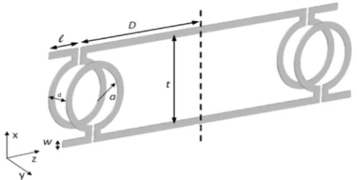
Recently, some of the authors have properly combined four regular omega resonators to build a symmetric structure, the so-called connected bi-omega particle, to obtain an interesting device with an inherent filtering behavior successfully em-ployed in novel microwave components, such as electrically small radiating apertures, waveguide filters, directional cou-plers, diplexers, power-splitters, etc. [26]–[29]. This particle consists of two bi-omega resonators, i.e., two regular equal omega resonators with mirror symmetry, connected together through their arms as shown in Figs. 1 and 2.
In order to predict the resonant frequencies of the connected bi-omega particle, in [27] a simple circuit model has been pro-posed and briefly described by the authors. That model turned out to be fairly accurate for the design in [27], although some 0018-926X © 2014 IEEE. Personal use is permitted, but republication/redistribution requires IEEE permission.
Fig. 2. Geometry of the connected bi-omega particle. Dashed line identifies the symmetry plane.
circuit elements were missing. For example, the capacitive re-actance of the gap between the dipole arms was not present, as well as the capacitive terms of the mutual coupling between the dipole and the dipole moment of the loop. In [27], the contribu-tion of such capacitances was likely compensated by assuming that the half-length of the transmission line connecting the two bi-omegas is counted from the end of one omega arm to the symmetry plane. However, as it is demonstrated in this paper, the correct assumption is the one considering the half-length of the transmission line from the center of the bi-omega particle to the symmetry plane (please, compare the line length in [27, Fig. 1] and Fig. 2). The open(short)-circuited stub, in fact, ex-hibits a higher capacitive (lower inductive) input reactance that compensates the missing capacitive terms. Due to these imper-fections, when fixing the values of the gap width and of the distance between the bi-omega particle and the symmetry plane, the validity of the model in [27] is strongly limited to a narrow range of the values of the arm length .
The aim of this paper, thus, is to propose a new and com-prehensive analytical model of both the bi-omega and the
con-nected bi-omega particle that overcomes the limitations due to
the approximations made in [27] and to provide, for the first time, a design procedure that allows retrieving the geometrical dimensions of the particle, starting from the desired resonant frequency. In this way, the design and application of the par-ticle in microwave components is significantly facilitated and new physical insights are also given for a better understanding of the particle operation.
The validity of the model is supported by proper full-wave simulations and experimental measurements conducted both in free-space and in metallic waveguides. In both scenarios, the electromagnetic response of the connected bi-omega particle does not change, demonstrating an interesting insensitivity of the particle to the surrounding environment.
The structure of the paper is as follows. In Section II, by exploiting the equivalent circuit representations of electrically small antennas [30], we first derive the equivalent circuit of the individual bi-omega particle. Then, by using symmetry consid-erations, in Section III we derive the equivalent network repre-sentation of the proposed connected bi-omega particle, which is used to estimate the resonant frequencies of the fundamental modes supported by the structure. In Section IV, we provide a design procedure of the proposed particle that allows designing the particle starting from the desired resonant frequencies. Fi-nally, in Section V, we verify the new proposed equivalent
cir-cuit models through proper full-wave numerical simulations and free-space and waveguide measurements.
II. BI-OMEGAPARTICLE: ANALYTICALMODEL Let us consider the individual bi-omega particle shown in Fig. 1. The particle is formed by the combination of a split-ring loop ( is the radius) and a dipole ( is the half-length). Ac-cording to Fig. 1, is the ring-dipole separation, is the width of the metallic strip, is the gap width, and is the separation between the two omegas. As previously anticipated, assuming that the bi-omega is electrically small, it is possible to use a quasi-static approach and estimate the electromagnetic behavior of the single-omega particle through a lumped-element equiva-lent circuit [31], [32].
The loop part of the omega, thus, can be considered as illumi-nated by a time-varying uniform field and, consequently, driven by a constant current. Under this assumption, the equivalent impedance of the small loop is given by the series of the mag-netic dipole radiation resistance and the single-turn loop self-inductance [30]
(1) (2) where , . and are the wave-number, the intrinsic impedance. and the permeability of the medium where the loop is placed, respectively, and the loop area.
Similarly, the arms of the omega act as a dipole driven by the current flowing in the loop. Being the dipole electrically small and the current null at the end of the arms, the current distribution can be considered linear. The equivalent impedance of the dipole connected to the loop, thus, is given by
(3) being
(4) where and are the permittivity and permeability of the sur-rounding medium, respectively.
Moreover, although the electric dipole moment of a stand-alone loop is often neglected, in the omega shape the loop is on the same plane of the dipole and, thus, their electric dipole mo-ments, i.e., the one of the loop and the one of the dipole, couple together modifying their electrical properties each other. The circuit model of the single omega, thus, has to take into account also the equivalent impedance of the electric dipole moment of the loop, which is obtained assuming that the equivalent dipole has the same length of the loop diameter
(5) (6) The resistive term is given by the radiation resistance of an electrically small dipole, as in (4), substituting the half-length of
the dipole with the radius of the loop. In fact, the dipole mo-ment of the loop is given by the distribution of opposite electric charges at the opposite points of the loop whose diameter is the total length of an equivalent electrically small dipole.
Looking at the loop-dipole connection, the metallic strips connecting the loop and the dipole are very close to each other and a coupling effect takes place [33] that can be described by the shunt capacitive impedance
(7) (8) where is the complete integral of the first kind and
To complete the circuit representation of the single omega, we need to model the mutual coupling between the dipole and the electric dipole moment of the loop of a single omega par-ticle. This term affects the resonant frequency of the particle, since the dipole and the loop are on the same plane. The mutual impedances and can be calculated through the method reported in [12], [30]
(9) where
(10) When two omega particles are placed very close to each other as shown in Fig. 1 in order to create the bi-omega particle, the mutual coupling effect between the two loops and the one be-tween the two dipoles come into play and needs to be modeled. The mutual impedance between the electric dipole moments of the dipoles and the loops of the two adjacent omegas can be again modeled properly setting the characteristic impedance in (9). We refer to these mutual impedances as , , , and where the subscript mm indicates the mutual imped-ances in presence of two omegas, and the superscripts iden-tify the parts of the omega (i.e., dipole or loop) involved in the coupling. Furthermore, the mutual impedance between the two loops is given by [34]
(11)
Finally, the electromagnetic excitation of the particle is mod-eled in terms of a voltage generator. According to the coordinate system shown in Fig. 1, we assume that the particle is excited only by a magnetic field , orthogonal to the loop plane. This
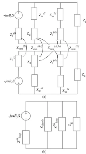
Fig. 3. Lumped element circuits: (a) complete circuit of two coupled omega particles—all the electric and magnetic coupling effects are reported. (b) Equiv-alent circuit of the bi-omega particle.
is the most common type of excitation used in the applications of the particle already proposed in the literature [26]–[29]. Under this assumption, the equivalent circuit is fed by an electromotive force e.m.f. induced on the loop portion of the omega particle by the variation of the magnetic flux density across the area of the loop
(12) In summary, the lumped element equivalent circuit repre-sentation of the two coupled omega particles is reported in Fig. 3(a).
This circuit reports the entire coupling effects between the different parts of the same omega and between the two adjacent omegas. Such a circuit can be simplified as shown in Fig. 3(b) where
Fig. 4. Equivalent circuit representation of the connected bi-omega particle reported in Fig. 2.
Once the equivalent circuit of the structure in Fig. 1 has been derived, it is possible to evaluate the induced current flowing on the particle as follows:
(14) where
(15) is the equivalent Thévenin impedance seen at the terminals of the voltage generator of Fig. 3(b).
In the following Section, we will consider the case of the con-nected bi-omega particle of Fig. 2 and modify the equivalent cir-cuit shown in Fig. 3(b), in order to take into account the trans-mission line that connects the two bi-omegas.
III. CONNECTEDBI-OMEGAPARTICLE: EVEN ANDODD MODEANALYSIS
Let’s consider now the connected bi-omega particle depicted in Fig. 2. The structure consists of two individual bi-omega particles connected through a transmission line having length equal to . As for any symmetric structure, we assume that the connected bi-omega particle supports two fundamental modes, having even and odd field symmetries, respectively. Such modes can be easily studied considering only half of the structure and terminating it on either a perfect magnetic or a perfect electric wall, respectively. This means that we just need to load the individual bi-omega particle with a transmission line stub with length terminated on a generic load impedance
that is either an open- or a short-circuit.
The corresponding circuit representation is reported in Fig. 4. According to the transmission line theory, thus, the imped-ances to add to the model of the individual bi-omega particle derived in Section II are
(16)
Fig. 5. Prospective view of the connected bi-omega particle printed on a di-electric slab.
being the characteristic impedance of the Lecher bifilar line [35] connecting the two bi-omega particles (Fig. 2)
(17) where is the effective permittivity defined later in (20).
Again, exploiting the circuit representation reported in Fig. 4, we are able to evaluate the current as function of the frequency when the transmission line is terminated on either a short- or an open-circuit
(18) where
(19) So far, we have considered the particles immersed in a given homogeneous medium (e.g., vacuum). However, when consid-ering the physical implementation of the structure, the metallic omegas are usually printed on the two opposite faces of a di-electric slab, as schematically shown in Fig. 5.
In order to take the presence of the dielectric slab into ac-count, we assume that the effective dielectric constant of the transmission line given by the two connected printed arms of the bi-omegas is the one of a regular suspended microstrip line [36]
(20) The equivalent circuit model of Fig. 4 can be used to predict the electromagnetic behavior of a realistic connected bi-omega particle. For instance, by using such representations, it is pos-sible to estimate the resonant frequencies of the two funda-mental modes supported by such a symmetric structure.
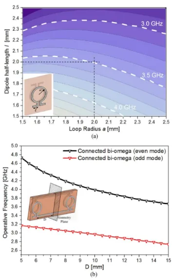
IV. DESIGN OF THECONNECTEDBI-OMEGAPARTICLE In this section, the proposed equivalent circuit model is used to design a connected bi-omega particle that has to operate at the desired even- and odd-mode resonant frequencies. To show an example of the design procedure, we consider a connected bi-omega particle that has to operate at 3 GHz (even-mode) and 4 GHz (odd-mode). In the following, we report the design pro-cedure and discuss all the choices taken throughout the design. Once the two desired resonant frequencies of the particle are given, we start the design by choosing the resonant frequency of the individual bi-omega particle. To this end, it is worth noticing that, in the case of the even mode of the connected bi-omega, the loading stub returns a capacitive impedance (open-circuit termi-nation) leading to a slight reduction of the resonant frequency of the individual bi-omega particle, whereas in the case of the odd mode, the loading stub returns an inductive impedance (short-circuit termination) which causes an increase of the resonant frequency in comparison to the one of the individual bi-omega particle. Therefore, the individual bi-omega particle has to res-onate at an intermediate frequency between the two ones of the connected bi-omega. In this example, we can fix it at 3.5 GHz. Then, we need to fix the substrate material on which the particle will be printed. In this case, we choose a thin dielectric board of Roger RO4003C with permittivity and thickness [37]. In order to evaluate the effective permit-tivity in (20), we have to set the width of the metallic strip, which is strictly related to the resolution of the technique used for the fabrication. Here, we consider using a milling machine for printed circuit boards, whose milling resolution is 0.25 mm. Similarly, we set the width of the gap and the distance be-tween the dipole and the loop. In order to be sure that the particle will be properly fabricated by the machine, we set , , and . Finally, using (14) we can plot the predicted resonant frequency of the individual bi-omega par-ticle, i.e., the maximum of the module of , as a function of the loop radius and the half-length of the dipole [see Fig. 6(a)]. Among the several combinations of and that make the par-ticle resonating at 3.5 GHz, we choose for having a more compact particle. However, other combinations are equivalent.
Afterwards, as mentioned in the introduction, in order to create the complete structure of Fig. 2, two identical indi-vidual bi-omegas are connected through a transmission line of half-length D, evaluated from one stem of one omega to the symmetry plane. As done in Fig. 6(a), by using (18) we report in Fig. 6(b) the resonant frequencies of the even and odd mode of the connected bi-omega particle, respectively, for different values of the line length D. The resonant frequency of both mode decreases for longer lines because the equivalent PMC/PEC plane recedes from the particle, which exhibits a longer effective resonant wavelength.
In the end, the connected bi-omega particle is characterized by the following geometrical parameters: , ,
, , , , and
being the slab parameters , .
In Table I, we report the values of the lumped elements of the
Fig. 6. (a) Resonant frequencies of the individual bi-omega particle as a func-tion of the loop radius a and the half-length of the dipole. Particle is printed on a substrate Roger RO4003C ( , ) and , , . (b) Resonant frequencies of the even and odd modes of the connected bi-omega particle as a function of the line length D.
TABLE I CIRCUITELEMENTSVALUES
omega particle. As mentioned in Section II, the resistive ele-ments are the radiation resistance of the loop and the dipole and, thus, they are frequency dependent quantities.
The two predicted resonant frequencies for the even and odd modes are 3.01 GHz and 4.03 GHz, respectively.
V. NUMERICAL ANDEXPERIMENTALVALIDATION In this Section, we report on the numerical and experimental validation of the connected bi-omega particle presented in
Fig. 7. Amplitude of the magnetic field at the centers of the loops in the cases of a slab placed in free-space and across a rectangular slit drilled in a metallic screen.
Section IV. We have simulated and measured the electromag-netic response of the connected bi-omega particle in free-space and in a metallic waveguide.
A. Validation Through a Free-Space Setup
In order to have a first validation of the equivalent circuit model, we have used a full-wave electromagnetic simulator, CST Studio Suite [38], to evaluate numerically the electromag-netic response of the connected bi-omega particle considered in the example at the end of Section III. The particle has been made of a 35- -thick copper metallization
printed on a Roger RO4003C dielectric board ( and ) [37] with dimensions
. In the simulations, the dielectric slab is placed in free-space and illuminated by a plane-wave with the unit-am-plitude magnetic field orthogonal to the loop plane, , and the electric field in the loop plane, (see Fig. 2 and the inset of Fig. 7).
At the resonant frequency, the current induced on the par-ticle is maximum and the same is also for the magnetic flux linked by the loop portion of the bi-omega particle. In the sim-ulations, we exploited this relationship and put two magnetic field probes at the centers of the loop pairs of each bi-omega particle to record the component of the magnetic field directed along the loop axes. The result of this exercise is represented by the solid-line plot shown in Fig. 7 (the two probes have given superimposed results and, thus, only one plot is shown in the figure).
Comparing the results of Figs. 6 and 7 (blue circles), we note a very good agreement in the positions of the resonant frequen-cies and comparable relative amplitudes between the induced currents and the probed magnetic field magnitudes. The opera-tive frequencies of the particle are 3.04 GHz and 3.97 GHz that are very close to the ones obtained through the design procedure. Then, in order to validate the model also when the connected bi-omega particle is in operative conditions, in Fig. 7 (solid line) we report also the amplitude of the magnetic field component at the centers of the loops when the particle is placed across a rectangular sub-wavelength aperture drilled in an infinitely extended metallic screen. The rectangular slit is 15 mm high and 3 mm wide. It is worth noticing that the response of the particle is not affected by the presence of the screen at all. We
Fig. 8. (a) Free-space measurement setup: the connected bi-omega particle is placed across a subwavelength aperture in a metallic screen. (b) Measured trans-mission enhancement as a function of the frequency.
have also changed the dimensions of the rectangular slit and used a finite (though large) metallic screen to check this point and the response obtained has not changed.
Then, we have fabricated a particle sample, being liable to the geometrical and material parameters used in the simulations. We have drilled the rectangular slit in a
aluminum screen and fixed the slab with the printed omegas across it, as shown in Fig. 8(a). The metal screen with the aper-ture has been placed between two identical standard horn an-tennas (WR 284 and WR 187 waveguide dimensions have been used to cover the frequency range between 3 and 6 GHz). The system has been calibrated setting the scattering param-eter equal to 0 dB when the metallic screen with the aperture is present. Then, the inclusion has been placed across the aper-ture and the transmission spectra have been acquired by using a vector network analyzer connected to the horn antennas. The ac-quired scattering parameter , thus, corresponds to the trans-mission enhancement factor due to the presence of the con-nected bi-omega particle across the aperture with respect to the case of the aperture alone. This result has been reported in Fig. 8(b).
Comparing the result in Fig. 8(b) to the corresponding ones shown in Fig. 7, we find a good agreement in the position of the maximums that represent the resonant frequencies of the particle. We highlight here that the peak magnitudes of the two modes cannot be compared to the ones in Fig. 7 because Fig. 8 shows the transmission enhancement with respect to the field magnitudes recorded during the calibration stage. Numerically
Fig. 9. Metallic screen with a drilled rectangular aperture is used to cover the cross section of a WR 90 waveguide. connected bi-omega particle is placed across the slit to get efficient transmission around its resonances.
speaking, in Fig. 8(b) the resonant frequency are 3.12 GHz and 3.91 GHz that are very close to the ones obtained through the circuit model and the numerical simulator, i.e., [3.01; 4.03] GHz and [3.04; 3.97] GHz, respectively.
B. Model Validation Through a Metallic Waveguide Setup
As shown in the previous section, the electromagnetic be-havior of the connected bi-omega particle is rather insensitive to the presence of the metallic screen and its frequency response is fairly predicted by the proposed analytical model. Here, we report the comparison between analytical, numerical, and exper-imental data when the particle is placed across a subwavelength aperture in a metallic screen that cover the cross section of a regular WR90 waveguide (Fig. 9).
A metallic screen with a drilled rectangular aperture is used to cover the cross section of a regular WR 90 waveguide (the theoretical cutoff frequency is 6.56 GHz). The idea is to design a connected bi-omega particle whose fundamental modes work within the mono-modal frequency range of the waveguide in such a way to obtain a frequency selective transmission. In the end, such a component is a filter, but it is presented in this frame-work just as an example of a waveguide component based on the proposed concept.
Assuming that the fundamental mode of the waveguide, i.e., , is propagating in the waveguide, the y-component of the guided magnetic field excites the connected bi-omega par-ticle. So, by using the design procedure described in Section IV,
the geometrical parameters are , ,
, , , ,
and , being the slab parameters ,
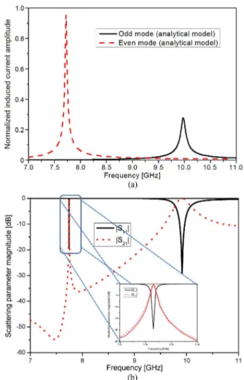
(Roger RO5880) [37]. The two resonant frequen-cies are expected to be at 7.70 GHz and 9.94 GHz for the even and the odd mode, respectively, that are in the mono-modal fre-quency band of the WR90 waveguide. The corresponding am-plitudes of the induced currents versus frequency are shown in Fig. 10(a).
Then, the electromagnetic behavior of such a connected bi-omega particle in a regular WR90 waveguide has been numerically studied by using CST Studio Suite [38]. The corresponding scattering parameters are shown in Fig. 10(b). Comparing the results of Fig. 10(a) and (b), it is possible to note that the frequency positions of the two peaks predicted by the analytical model [Fig. 10(a)] and of the two deeps of the transmission coefficient [Fig. 10(b)] agree very well. This result further confirms that the particle is rather in-sensitive to the variation of the surrounding environment, since the analytical model assumes that the particle is in free-space.
Fig. 10. (a) Magnitude of the induced current in the cases of even and odd op-eration modes computed through the analytical model developed in Section III. (b) Magnitude of the simulated scattering parameters for the structure shown in Fig. 9.
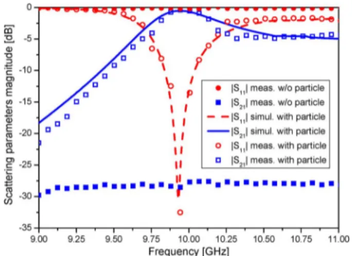
After the numerical verification of the efficient transmission at the resonant frequencies of the two fundamental modes of the connected bi-omega particle, we have conducted also the exper-iments. Considering that the suggested operation range of the WR 90 waveguide is 8.2–12.4 GHz, the first resonance at 7.67 GHz (though being above the theoretical cutoff of the wave-guide) cannot be accurately measured. Therefore, we have fo-cused our attention on the second resonance only (i.e., the one at 9.94 GHz). After a proper TRL calibration of the measure-ment setup at the sample holder section, we have measured the scattering parameters at the two ports of the waveguide by using a vector network analyzer in two cases: 1) presence of the slotted screen only; 2) presence of the screen with the connected bi-omega particle fixed across the slit. In Fig. 11, we show the comparison between the experimentally measured and the nu-merically computed scattering parameter magnitudes in the fre-quency range 9–11 GHz. Again, the agreement between numer-ical and experimental results is very good. It is worth noticing that, differently from the results in Fig. 10(b) obtained by sidering the omega metallization made of a perfect electric con-ductor, the simulated results shown in Fig. 11 have been ob-tained by assuming the omega metallization made of copper . Simulated and measured insertion loss
Fig. 11. Comparison between simulated and measured magnitudes of the scat-tering parameters of the waveguide depicted in Fig. 9.
at the resonant frequency of the odd mode (9.94 GHz) is almost identical and equal to 0.4 dB.
In the end, we can conclude that the proposed particle is rather insensitive to the variations of the surrounding environment, i.e., free-space, across an infinitely extended metallic screen, or in a waveguide. In fact, it is worth noticing that the par-ticle has been designed in Section IV without taking into ac-count the presence of the metallic screens and by using a set of equations that assumes the free-space condition. This behavior can be explained considering the geometrically balanced and symmetrical structure of the connected bi-omega particle, that makes it a good candidate for the realization of a novel family of filtering microwave components [26]–[29] whose operative frequency (given by the resonant frequency of the particle) must be predicted accurately before the actual realization of the mi-crowave component.
VI. CONCLUSIONS
In this paper, we have proposed a new analytical model of both the bi-omega and the connected bi-omega particles. The model is based on an equivalent circuit representation and al-lows calculating the resonant frequencies and, thus, the elec-tromagnetic response of the particle. The proposed model has been exploited to estimate the resonant frequencies of the two supported fundamental modes of the connected bi-omega par-ticle, having even and odd symmetries, respectively. In addition, we have developed and described an effective design procedure based on the proposed circuit model that guides to the actual realization of the particle once the desired resonant frequencies are given. Comparing the resonant frequencies obtained through the equivalent circuit analysis and both full-wave numerical and experimental results, an excellent agreement has been found, confirming the validity and the accuracy of the proposed model and of the design guide.
REFERENCES
[1] D. L. Jaggard, A. R. Mickelson, and C. H. Papas, “On electromagnetic waves in chiral media,” Appl. Phys., vol. 18, pp. 211–216, 1979. [2] D. L. Jaggard, N. Engheta, M. N. Kowarz, P. Pelet, J. C. Lin, and Y.
Kim, “Periodic chiral structures,” IEEE Trans. Antennas Propag., vol. AP-37, no. 11, pp. 1474–1452, Nov. 1989.
[3] D. L. Jaggard and N. Engheta, “Chirality in electrodynamics: Modeling and applications,” in Directions in Electromagnetic Wave Modeling. New York, NY, USA: Plenum, 1991.
[4] I. V. Lindell, A. H. Sihvola, S. A. Tretyakov, and A. J. Viitanen,
Elec-tromagnetic Waves in Chiral and Bi-Isotropic Media. Norwood, MA,
USA: Artech House, 1994.
[5] , A. Priou, A. Sihvola, S. Tretyakov, and A. Vinogradov, Eds.,
Advances in Complex Electromagnetic Materials. Dordrecht, The
Netherlands: Kluwer, 1997.
[6] S. A. Tretyakov and A. A. Sochava, “Eigenwaves in uniaxial chiral omega media,” Microwave Opt. Technol. Lett., vol. 6, pp. 701–705, 1993.
[7] S. A. Tretyakov and A. A. Sochava, “Proposed composite material for non-reflecting shields and antenna radomes,” Electron. Lett., vol. 29, pp. 1048–1049, 1993.
[8] S. A. Tretyakov, “Thin pseudochiral layers: Approximate boundary conditions and potential applications,” Microw. Opt. Technol. Lett., vol. 6, pp. 112–115, 1993.
[9] A. N. Serdyukov, I. V. Semchenko, S. A. Tretyakov, and A. Sihvola,
Electromagnetics of Bi-Anisotropic Materials: Theory and Applica-tions. Amsterdam, The Netherlands: Gordon and Breach Science,
2001.
[10] F. Bilotti, A. Toscano, and L. Vegni, “FEM-BEM formulation for the analysis of cavity backed patch antennas on chiral substrates,” IEEE
Trans. Antennas Propag., vol. 51, no. 2, pp. 306–311, Feb. 2003.
[11] F. Bilotti, L. Vegni, and A. Toscano, “Radiation and scattering features of patch antennas with bianisotropic substrates,” IEEE Trans. Antennas
Propag., vol. 51, no. 3, pp. 449–456, Mar. 2003.
[12] S. A. Tretyakov, F. Mariotte, C. R. Simovski, T. G. Kharina, and J. He-liot, “Analytical antenna model for chiral scatterers: Comparison with numerical and experimental data,” IEEE Trans. Antennas Propag., vol. 44, no. 7, pp. 1006–1014, Jul. 1996.
[13] C. R. Simovski, S. A. Tretyakov, and A. A. Sochava, “Antenna model for conductive omega particles,” J. Electromagn. Waves Applicat., vol. 11, pp. 1509–1530, 1997.
[14] M. M. I. Saadoun and N. Engheta, “A reciprocal phase shifter using novel pseudochiral or omega medium,” Microw. Opt. Technol. Lett., vol. 5, pp. 184–188, 1992.
[15] F. Bilotti and L. Sevgi, “Metamaterials: RF and microwave applica-tions,” Int. J. RF Microw. C. E., vol. 22, no. 4, p. 421, July 2012. [16] J. B. Pendry, “A chiral route to negative refraction,” Science, vol. 306,
pp. 1353–1355, 2004.
[17] B. Wang, J. Zhou, T. Koschny, and C. M. Soukoulis, “Nonplanar chiral metamaterials with negative index,” Appl. Phys. Lett., vol. 94, p. 151112, 2009.
[18] J. Zhou, J. Dong, B. Wang, T. Koschny, M. Kafesaki, and C. M. Souk-oulis, “Negative refractive index due to chirality,” Phys. Rev. B, vol. 79, p. 121104, 2009.
[19] Y. Ra’di, V. S. Asadchy, and S. A. Tretyakov, “Total absorption of electromagnetic waves in ultimately thin layers,” IEEE Trans.
Antennas Propag., vol. 61, no. 9, pp. 4606–4614, Sep. 2013.
[20] S. M. Hashemi, M. Soleimani, and S. A. Tretyakov, “Compact neg-ative-epsilon stop-band structures based on double-layer chiral inclu-sions,” IET Microw. Antennas Propag., vol. 7, no. 8, pp. 621–629, Aug. 2013.
[21] J. Vehmas, Y. Ra’di, A. O. Karilainen, and S. Tretyakov, “Elimi-nating electromagnetic scattering from small particles,” IEEE Trans.
Antennas Propag., vol. 61, no. 7, pp. 3747–3756, Jul. 2013.
[22] Y. Ra’di and S. A. Tretyakov, “Balanced and optimal bianisotropic particles: Maximizing power extracted from electromagnetic fields,”
New J. Phys., vol. 15, p. 053008, 2013.
[23] J. Huangfu, L. Ran, H. Chen, X. Zhang, K. Chen, T. M. Grzegor-czyk, and J. A. Kong, “Experimental confirmation of negative refrac-tive index of a metamaterial composed of -like metallic patterns,”
Appl. Phys. Lett., vol. 84, p. 1537, 2004.
[24] L. Ran, J. Huangfu, H. Chen, Y. Li, X. Zhang, K. Chen, and J. A. Kong, “Microwave solid-state left-handed material with a broad bandwidth and an ultralow loss,” Phys. Rev. B, vol. 70, p. 073102, 2004. [25] A. Sihvola, Electromagnetic Mixing Formulas and Applications, ser.
Electromagnetic Wave. London, U.K.: Inst. Electr. Eng., 1999. [26] L. Di Palma, F. Bilotti, A. Toscano, and L. Vegni, “Design of a
wave-guide diplexer based on connected bi-omega particles,” IEEE Microw.
Wireless Compon. Lett., vol. 22, no. 3, pp. 126–128, 2012.
[27] F. Bilotti, L. Di Palma, D. Ramaccia, and A. Toscano, “Self-filtering low-noise horn antenna for satellite applications,” IEEE Antennas
Wireless Propag. Lett., vol. 11, pp. 354–357, 2012.
[28] L. Di Palma, F. Bilotti, A. Toscano, and L. Vegni, “Design of a wave-guide power splitter based on the employment of bi-omega resonators,”
Microw. Opt. Technol. Lett., vol. 54, no. 9, pp. 2091–2095, 2012.
[29] D. Ramaccia, L. Di Palma, G. Guarnieri, S. Scafè, A. Toscano, and F. Bilotti, “Balanced and unbalanced waveguide power splitters based on connected bi-omega particles,” Electron. Lett., vol. 49, no. 24, pp. 1504–1506, 2013.
[30] S. A. Schelkunoff and H. T. Friis, Antennas Theory and Practice. New York, NY, USA: Wiley, 1952.
[31] F. Bilotti, A. Toscano, and L. Vegni, “Design of spiral and multiple split-ring resonators for the realization of miniaturized metamate-rial samples,” IEEE Trans. Antennas Propag., vol. 55, no. 8, pp. 2258–2267, Aug. 2007.
[32] F. Bilotti, A. Toscano, L. Vegni, K. B. Alici, K. Aydin, and E. Ozbay, “Equivalent circuit models for the design of metamaterials based on artificial magnetic inclusions,” IEEE Trans. Microw. Theory Tech., vol. 55, no. 12, pp. 2865–2873, Dec. 2007.
[33] S. Gevorgian and H. Berg, “Line capacitance and impedance of coplanar-strip waveguide on substrates with multiple dielectric layers,” presented at the Microwave Conf. 2001, London, U.K., Sep. 2001.
[34] A. N. Lagarkov, V. N. Semenenko, V. A. Chistyaev, D. E. Ryabov, S. A. Tretyakov, and C. R. Simovski, “Resonance properties of bi-helix media at microwaves,” Electromagnetics, vol. 17, no. 3, pp. 213–237, 1997.
[35] E. Lecher, “Eine Studie über electrische Resonanzerscheinungen,”
An-nalen der Physik, vol. 277, no. 12, pp. 850–870, 1890.
[36] I. Bahl and P. Barthia, Microwave Solid State Circuit Design, 2nd ed. New York, NY, USA: Wiley-Interscience, 2003.
[37] Roger Corporation [Online]. Available: http://www.rogerscorp.com/ [38] CST Studio Suite 2013 CST Computer Simulation Technology
[On-line]. Available: http://www.cst.com
Davide Ramaccia (S’11–M’12) was born in Rome,
Italy, on April 23, 1985. He received both the B.S. (summa cum laude) and M.S. (summa cum laude) de-grees in electronic and ICT engineering from Roma Tre University, Rome, Italy, in 2007 and 2009, re-spectively. In 2013, he received the Ph.D. degree in electronic engineering from the same university.
Since 2012, he is with the Department of Engi-neering, Roma Tre University. His main research interests are in the microwave and optical compo-nents loaded with complex media, metamaterials, and metasurfaces.
Dr. Ramaccia has been member of the local committee of the Fifth Italian Workshop on Metamaterials and Special Materials, Meta 2010 (Rome, Italy, De-cember 2010) and, also, he was secretary member of the fourth Italian Workshop on Finite Element Methods applied to Electrical and Information Engineering, FEM 2010 (Rome, Italy, December 2010). He currently serves as a Technical Reviewer of the major international journals related to electromagnetic field theory and metamaterials. He is currently Secretary of the Virtual Institute for Artificial Electromagnetic Materials and Metamaterials (METAMORPHOSE VI, the International Metamaterials Society). He is currently member of the Italian Society on Electromagnetics, SIEM, and of the National Inter-Univer-sity Consortium for Telecommunications, CNIT. He received the IET Award for the Best Poster on the Metamaterial Application in Antenna Field in 2011 and the third IET prize for the best poster on microwave metamaterials in 2013.
Luca Di Palma was born in Rome, Italy, in 1987.
He received the B.S. degree in electronic engineering (summa cum laude) and the M.S. degree in ICT engi-neering (summa cum laude) from the University of Roma Tre, Rome, Italy, in 2009 and 2011, respec-tively. He is currently pursuing the Ph.D. degree in signal processing and telecommunication systems at the University of Rennes 1, Rennes, France.
Since 2013, he has been a Research Assistant at CEA-LETI, Grenoble, France. His research interests include metamaterials and quasi-optic reconfigurable antennas at microwave frequencies.
His master thesis project on the design of waveguide components loaded with metamaterials was awarded a special mention at the Marconi Junior Prize in 2012.
Damla Ates, photograph and biography not available at the time of publication.
Ekmel Ozbay, photograph and biography not available at the time of
publication.
Alessandro Toscano (S’90–M’95–SM’11) was born
in Capua on 26 June, 1964. He received the Laurea and the Ph.D. degrees in electronic engineering from the University La Sapienza, Rome, Italy, in 1988 and 1993, respectively.
After a brief postdoctoral research experience at the Italian Space Agency, in 1994, he joined the De-partment of Applied Electronics at the University of Roma Tre, Rome, where is now Professor of Electro-magnetic Field Theory. His current research interests are computational electromagnetics and nonconven-tional materials and metamaterials for microwave and optical applications.
Prof. Toscano is (co-)author of more than 200 peer-reviewed scientific papers.
Filiberto Bilotti (S’97–M’02–SM’06) received the
laurea and Ph.D. degrees in electronic engineering from Roma Tre University, Rome, Italy, in 1998 and 2002, respectively.
Since 2002, he has been with the Department of Engineering, Roma Tre University, where he is an Associate Professor of electromagnetic field theory. His main research interests are in the microwave and optical applications of complex media, metama-terials, and metasurfaces. He is the author of more than 370 papers in international journals, conference proceedings, and book chapters.
He is a member of the Steering Committee of the European Doctoral School on Metamaterials and the organizer of several international school events and international workshops and conferences in the field of metamaterials. He has been the local organizer of the First Congress on Advanced Electromagnetic Materials and Metamaterials in Microwaves and Optics-Metamaterials 2007 (Rome, Italy, October 2007) and served as the Chairman of the Steering Committee of the same conference for the period 2008–2014. He served also as a member of the technical program, steering and organizing committees of several national and international conferences, as organizer and chairman of special sessions focused on the applications of metamaterials at microwave and optical frequencies, as a member of the Editorial Board of the
Interna-tional Journal on RF and Microwave Computer-Aided Engineering, Scientific Reports—Nature, and EPJ Applied Metamaterials, as an Associate Editor of
the IEEE TRANSACTIONS ONANTENNAS ANDPROPAGATION(2013-present) and Metamaterials (2007–2013), and as a Technical Reviewer of the major international journals related to electromagnetic field theory and metamaterials. He was an elected member of the Board of Directors (2007–2013) and currently is the President (2013–2016) of the Virtual Institute for Artificial Electromag-netic Materials and Metamaterials (METAMORPHOSE VI, the International Metamaterials Society). He is a Member of the Optical Society of America. He received the Raj Mittra Travel Grant Senior Researcher Award in 2007.