ELECTÄO^l FHOTDSMâ^fOM DETECTORS
lî W ,ы -Vî-'sî^.M'rTsrn -f^'·. --Wir
OF PHYSÎ03
·'0
‘ - r . - ’'¿ «л% .‘ ^ Ѣ «. ■ .-»«ιίί'Д . w *< F·^ wч^'f^ .-' ■' D· ^ 'D- ■' T Τ'^UTT;"·,:/; *^4 F 5 '* ■» " I f · •'■««««І! - \ * ^ · фтт^ о· «hwΫ.'· V 'і^'лЛтет^ 'V «і •4**^··,·'*^ tT İt ¿ -* ί Ι » *r )*<>*^-*··1ι«ί^·^'»4»'* *.' « Τ ’ 4iÍ^^'afJ¿D^j>> Q . ^ · ^ П '^ С i* «U»'& \k я; к «ÀM ^ °·' •^■■: ѵ-г-гч, '4ü<^.4« ' . ;'î *·' «'W - .«.ѵГ^к '%>>· Ц цО »-»τ'« ¡(O·» îİ*« Ц:?^Л! i K ’ b ’ ıc * '#>·* »i 4 · «i 4 >' * · V * · . * “«ішг;» i *. л i иLONG W AVELENGTH GAAS BASED HOT
ELECTRON PHOTOEMISSION DETECTORS
A THESIS
SUBMITTED TO THE DEPARTMENT OF PHYSICS AND THE INSTITUTE OF ENGINEERING AND SCIENCE
OF BILKENT UNIVERSITY
IN PARTIAL FULFILLMENT OF THE REQUIREMENTS FOR THE DEGREE OF
MASTER OF SCIENCE
By
Ibrahim Kimukin
July 1999
■ M b \333
I certify that I have read this thesis and that in my opinion it is fully adequate, in scope and in quality, as a dissertation for the degree of Master of Science.
Assoc. Prof. E k m e ^ a b a y (Supervisor) I certify that I have read this thesis and that in my opinion it is fully adequate, in scope and in quality, as a dissertation for the degree of Master o f Science.
I certify that I have read this thesis and that in my opinion it is fully adequate, in scope and in quality, as a dissertation for the degree of Master of Science.
Assoc. Prof. Orhan Arikan
Approved for the Institute o f Engineering and Science:
Prof. Mehmet Bara}^
LO N G W A V E L E N G T H G A A S BA SED H O T
ELEC TR O N PH O TO E M ISSIO N D E TE C TO R S
Ibrahim Kimukin
M. S. in Physics
Supervisor: Assoc. Prof. Ekmel Ozbay
July 1999
The increasing rate of telecommunication alters both science and technology, and demands high performance components. Photo detectors are essential components of optoelectronic integrated circuits and fiber optic communication systems. A new family of photodetectors offer high performance along with wavelength selectivity: resonant cavity enhanced (RC E) photodetectors.
In this thesis, we present our efforts for design, fabrication and characterization of GaAs/AIGaAs based Schottky photodetectors operating within the first (850 nm) and second (1300 nm) optical communication windows. Epitaxial wafers are designed using transfer matrix method based simulation and are grown with molecular beam epitaxy. The photodetector operating at 840 nm was designed with indium tin oxide (IT O ) Schottky layer for high quantum efficiency. The second photodetector is based on internal photoemission, and is compatible with advanced GaAs process technology. Our aim with this design is high speed operation at the second optical communication window. We measured 20 GHz 3-dB bandwidth with 60% quantum efficiency at 840 nm. W e expect 50 GHz 3-dB bandwidth with 0.05% quantum efficiency at 1310 nm.
Keywords: Resonant Cavity, Resonant Cavity Enhancement, Schottky pho todetector, Internal Photoemission, High Speed, High Quantum Efficiency, Bandwidth-Efficiency Product
GAAS
t e m e l l iUZUN DALGABOYLARINDA ÇALIŞAN
SICAK ELEKTRON FOTOEMİSYON DETEKTÖRÜ
İbrahim Kimukin
Fizik Yüksek Lisans
Tez Yöneticisi: Doç. Dr. Ekmel Özbay
Temmuz 1999
İletişim alanındaki hızlı gelişme bilim ve teknolojiyi etkilemekte, ve yüksek per
formanslı aygıtlara ihtiyaç duymaktadır. Fotodetektörler optoelektronik tümleşik
devre ve optiklif iletişim sistemlerinin vazgeçilmez elemanlarıdır. Resonans çınlaç
arttırımlı (RC E) fotodetektörler yüksek performansla beraber dalgaboyu seçimini sunmaktadır.
Bu tezde GaAs/AlGaAs temelli, birinci (850 nm) ve ikinci (1300 nm) optiklif iletişim penceresinde çalışan Schottky fotodetektörlerin tasarım, üretim, ve karak-
terizasyonunu sunmaktayız. Diyot yapılarının tasarımı transfer matris yöntemine
dayalı simulasyon ile yapıldı ve moleküler ışın büyütme tekniğiyle büyütüldü. 840 nm de çalışan fotodedektörde kuvantum verimini arttırmak için Schottky tabakası indiyum kalay oksit (IT O ) ile büyütüldü. İkinci detektör gelişmiş GaAs prosesine uygun, iç fotoemisyon kullanarak tasarlandı. Bu tasarımki amacımız yüksek hız ve ikinci optiklif iletişim penceresinde çalışmak idi. Ölçümlerimizde 840 nm de çalışan dedektörde 20 GHz 3-dB bantgenişliği ve % 60 kuvantum verimi elde ettik. 1310 nm de çalışan dedektörde 50 GHz bantgenişliği ve % 0.05 kuvantum verimi beklemekteyiz.
Anahtar
sözcükler: Resonant Çınlaç, Resonant Çınlaç Arttırım ı, Schottky Fotodetektör, İç Fotoemisyon, Yüksek Hız, Yüksek Kuvantum Verimi, Hız-verim Çarpımı
It is my pleasure to express my deepest gratitude to my supervisor Assoc. Prof. Ekmel Ozbay for his guidance, helpful suggestions and fruitful discussions throughout my thesis work. I have not only benefited from his wide spectrum of interest in physics, but also learned a lot from his superior academic personality.
I would like to thank to all members of physics department and advanced research laboratory, especially Necmi Bıyıklı who taught me everything, I know about GaAs processing, Mehmet Bayındır who helped me write this manuscript. I also want to thank Murat Güre who helped me during my semiconductor device processes.
I wish to thank Assoc. Prof. M. Selim Ünlü, Mutlu Gökkavas and Gökhan Ulu of Boston University for their efforts in high speed measurements of our devices.
Contents
Abstract i Özet i Acknowledgement i Contents i List of Figures iv List of Tables vi 1 Introduction 1 2 Theoretical Background 42.1
Schottky Photodiode O p e r a tio n ... 42.1.1
Schottky Junction 52.1.2
Detector O p e ra tio n ... 72.1.3 Diode P erform a n ce...
11
2.2 Internal Photoernission... 13
2.3 Resonant Cavity Enhancement... 15
2.3.1 RCE Form ulation... 17
2.3.2 Standing Wave E ffe c t... 18
3.2
Device Sim ulation... 253.3 Cavity D e s ig n ... 28
3.4 NIST S a m p l e ... 30
3.4.1 Design and O ptim ization... 30
3.4.2 Reflectivity Characterization... 32
3.5 ISU S a m p l e ... 34
3.5.1 Design and O ptim ization... 34
3.5.2
Reflectivity Characterization... 35Fabrication 37 4.1 Standard P ro c e s s e s ... 37
4.1.1 Cleaving and Wafer Cleaning 37 4.1.2 P h otolith ograph y... 38
4.1.3 E t c h i n g ... 39
4.1.4 M etalization... 41
4.1.5 A n n e a lin g ... 41
4.1.6 Plasma Enhanced Chemical Vapor D e p o s itio n ... 42
4.1.7 Indium Tin Oxide D e p o s it io n ... 42
4.1.8 Lift-off·... 42
4.2
F a b r ic a t io n ... 434.2.1 Ohmic Contact F o rm a tio n ... 43
4.2.2 Mesa Isolation... 43
4.2.3 Interconnect Metalization 43 4.2.4 Schottky Contact F orm ation... 44
4.2.5 Dielectric D e p o s itio n ... 44
4.2.6 Airpost Formation 44 4.2.7 Airbridge M eta liza tion ... 46
4.2.8 Top Mirror D e p o s itio n ... 46
5 Measurements 48
5.1 IV M easurem ents... 48
5.2 Quantum Efficiency Measurements 49 5.2.1 NIST S a m p l e ... 50
5.2.2
ISU S a m p le ... 525.3 High-Speed M easurem ents... 53
5.3.1 NIST S a m p l e ... 55
5.3.2 ISU S a m p le ... 55
6 Achievements and Future Directions 56
2.1 Energy band diagram of a Schottky ju n c t io n ... ... . 5
2.2
Photogenerated carriers inside the depletion l a y e r ... 72.3 The carriers generated at a; = xg induce output current as they move across the depletion reg ion ...
8
2.4 The induced current as a function of time
10
2.5 Expected output current for a uniformly illuminated diode where hole drift velocity is smaller than the electron drift velocity . . . .10
2.6
(a)Schematics of the photodiode circuitry (b)Equivalent circuit model for high frequency a n a ly s is ...12
2.7 Excitation of en electron in the internal photoemission 13
2.8
Analysis model of an RCE p h otod etector... 162.9
QE for different top DBR reflectivities (Rj) for ad = 0.1 and R2
= 9 9 .9 9 % ... 192.10 QE spectrum for different top DBR reflectivities (Ri) for ad = 0.1 and R2 = 9 9 .9 9 % ... 20
2.11 QE spectrum for different
ad with DBR reflectivities Ri = 78.9% and R2 = 9 9 .9 9 % ...21
3.1 Electric fields at the interface 26 3.2 Electric field inside a l a y e r ... 27
3.3 Electric fields outside our s t r u c tu r e ... 28
3.4 Reflectivity of DBRs used in NIST and ISU sam ples... 29
3.5 Epitaxial design of NIST sam ple... 31
3.6 3.7 3.8 3.9 4.1 4.2 4.3 4.4 4.5 5.1 5.2 5.3 5.4 5.5 5.6
Measured (solid line) and simulated (dotted line) reflectivity of NIST sample ...
33
Epitaxial design of ISU sam ple... 34 Measured (solid line) and simulated (dotted line) reflectivity of ISU s a m p l e ... 35 Crosssection of ISU sample taken with S E M ... 36 Resist profile of normal and image-feversal photolithography . . . 39 SEM image o f wet-etch p r o file ... 40 SEM photograph of an airbridge... 45Crosssection of an airbridge 45
Photograph of complete d e v ice ... 47
Current-Voltage characteristics of ISU sample 49
Simple diagram of quantum efficiency setup ... 50 Experimental (solid line) and theoretical (dotted line) Quantum Efficiency o f NIST sample for different top DBR pair number 51 Experimental (solid line) and theoretical (dotted line) Quantum Efficiency of ISU s a m p l e ... 52 Simple diagram of high speed s e t u p ... 53
Introduction
“The new era in communications began with the desire of loved ones to stay in touch with GIs scattered across the United States and dozens of countries around the world. That, combined with the government’s military communications need, spawned the habit of ’reaching out’ by phone” says Amos Joel, who was awarded the National Medal of Technology by the President of the USA in 1993. The invention of the telephone by Alexander Graham Bell lead to an enormous world wide communication market, which earns 1.5 trillion dollar each year. The unexpected demand for calling services during and after the second world war continued and began to strain the most modernized telephone network.
The invention of the first solid-state transistor in 1947, opened the age of computing and communication. In 1960’s researchers developed the first laser. The development of the first commercially feasible optical fiber in 1970’s made the fiber optic communication a promising candidate for telecommunication. In the early 1980’s satellites capable of carrying nearly
100,000 simultaneous calls
are used for telephone calls. Demand for the faster, cheaper, and less noisy communication made the first transatlantic undersea fiber-optic telephone cable possible that replaced the copper one that had been installed in 1956. That was the first fiber-optic revolution in telecommunication.The second revolution came with the introduction of wavelength division multiplexing (W DM ). Telephone companies had laid cable containing 24 to 36
CHAPTER 1. INTRODUCTION
fibers with 2.5 G bit/s rate, many had been reserved as “dark fiber” . But the tremendous traffic has crowded these cables that once seemed so voluminous. In the mid 1990’s, companies began using systems capable of transmitting at four wavelengths, and soon this number increased to eight.
Due to the properties of the commercial silica based fibers, optoelectronic research focused at three wavelengths, where the minimum atennuation occurs.^ First one is located at 850 nm, which is called the first optical window. GaAs based detectors are usually used for the detection. Local area networks use this window, because of the high loss in this window. The second and the third windows are located at 1310 and 1550 nm respectively. The loss in these wavelengths is much less than the first optical window, hence they are used for long distance fiber optic communication.
Lasers, modulators, photodetectors, optical amplifiers, and optical fibers are the main components of an optical communication system. The optical fiber offers an operation bandwidth up to tens of THz. The research effort in optoelectronics is devoted to fully exploit the fiber bandwidth. This can be possible with high performance components.
Semiconductor based photodiodes demonstrate excellent features to fulfill the requirements of high speed optoelectronic receiver. GaAs is the most studied material for photodetection. GaAs based Schottky and p-i-n detectors have been demonstrated bandwidth capabilities as high as 200 G H z ."^ U s in g low temperature grown GaAs, photodetectors with bandwidths up to 550 GHz have been fabricated.^ However, the efficiencies of these detectors have been less than
10%, due to thin absorption layer needed for short transit time.
Resonant cavity enhanced (RCE) photodetectors offer the possibility i)f overcoming this limitation of bandwidth-efficiency product of conventional p h o t o d e t e c t o r s . T h e RCE photodetectors are based on the enhancement of the optical field inside a Fabry-Perot cavity. This enhancement allows the usage of thinner active layers, which minimizes the transit time without sacrificing the quantum efficiency. RCE detector research is mainly concentrated in three typois of detectors; Schottky, p-i-n, and avalanche photodiodes.
100
GHz bandwidthand 25 GHz bandwidth-efficiency product Schottky diodes have been reported. 46 GHz bandwidth-efficiency product p-i-n photodetector with 92% quantum efficiency has been reported.®
Chapter
2
reviews the theory of Schottky diode, its application as photode tector and its current-voltage characteristics. We also examine the transport of carriers, and the high speed design. We also present the theory o f internal photoemission, and wavelength dependence of the quantum efficiency in this effect. We conclude that chapter with the theory of resonant cavity enhancement (RCE) and present the simulation results of the RCE photodetectors.Chapter 3 contains detailed description of our simulation technique, design parameters of our photodetectors. We also show comparison of our simulated and measured reflectivities of our molecular beam epitaxy grown samples. A brief list o f semiconductor materials used in the photodetector designs in different part of the spectrum is also given.
In chapter 4, we present the standard GaAs processing and techniques. We describe our fabrication steps, and process parameters.
Chapter 5 describes the characterization of the fabricated photodetectors. We discuss the measurement of current-voltage characteristics, quantum efficiency, and high-speed measurements. Also the experimental setup used in these measurements are explained and the comparison between the simulations and the measurements is given.
In chapter
6, we present our results, and the improvements can be made to
get better results. We also mention our future plans.Chapter 2
Theoretical Background
Photodetectors can be classified into two categories: thermal detectors and quantum detectors. Thermal detectors sense the radiation by its heating effect. Thermal detectors have the advantage of wide spectral range and operation at the room temperature, but they are limited as far as speed and sensitivity are concerned. Bolometers, thermistors, pyroelectric detectors are widely used thermal detectors. Operation of quantum detectors depend on the discrete nature of photons which can transfer energy of individual particles (electron and hole) giving rise to a photocurrent. These devices are characterized by very high sensitivity, high speed but limited spectral response. Photoernissive, photovoltaic, and photoconductive detectors are classified in this category. The conductivity change in the photoconductive detectors is proportional to the intensity of the radiation falling on the semiconductor. Rectifying junctions are the basis of the photovoltaic detectors. Under the illumination, the excess carriers created within
Hi'iiiicoiiductor giîiieraie a proiiortioiial outiMit cuiToiit.
2.1
Schottky Photodiode Operation
The theory of rectification in metal-semiconductor junction was developed in 1930;s by W. Schottky who attributed rectification to a space-charge layer in the semiconductor.^’^ Schottky photodiodes are widely used for high sp(!ed
EC
Figure
2.1; Energy band diagram of a Schottky junction
applications.
2.1.1
Schottky Junction
A Schottky diode consists of a metal-semiconductor junction. Figure
2.1 shows
the energy band diagram after the contact is made and equilibrium has been reached. When the two substances are brought into intimate contact electrons from the conduction band of the semiconductor, which have higher energy than the electrons in the metal, flow into the metal. This process continues until the Fermi level on both sides is brought into coincidence. As the electrons move from semiconductor to metal, the free electron concentration in the semiconductor region near the boundary decreases. The length of this region is given by®:W = /
2
eqN,i{Vu - V) (2.1)
where e is the dielectric constant of the semiconductor, is the ionized donor atom density, Yu is the built-in potential in the semiconductor, and the V
CHAPTER 2. THEORETICAL BACKGROUND
is the applied potential to the junction. Since the separation between the conduction band edge Ec and the Fermi level E;;· increases with decreasing electron concentration and in thermal equilibrium Ef- remains constant, the conduction band edge bends up. The conduction band electrons which cross over the metal leave a positive charge of ionized donor atoms behind, so the semiconductor region near the metal gets depleted of mobile electrons. Consequently an electric field is established from the semiconductor to the metal. The build-in potential due to that electric field is
gVi (
2
.2
)the difference of the work function of metal and semiconductor. The potential and electric field as a function of the distance from the junction are given by:
(/j(.x) = gKd ' 2e w u i -E {x) = - d(j){x) X W (2,3) (2.4) dx e
The current transport in the metal-serniconductor contacts is mainly due to majority carriers, in contrast to p-n junctions. There are four different mechanisms by which the carrier transport can occur: (1) thermionic emission over the barrier, (2) tunneling through the barrier, (3) carrier recombination (or generation) in the depletion region, and (4) carrier recombination in the neutral region of the semiconductor. Usually the first process is the dominant mechanism in Schottky barrier junctions in Si and GaAs and leads to the ideal diode characteristics.
Thermionic emission theory is derived by Bethe^“^ for high-mobility semi conductors, and diffusion theory is derived by Schottky^“ for low-mobility semiconductors. A synthesis of the thermionic emission and diffusion approaches has been proposed by Crowell and Sze.^^ The complete expression of the J-V characteristics is given by:
J Js J^<lV/kT _ A**T^exp - q(l>Bn kT (2.5) (2.6)
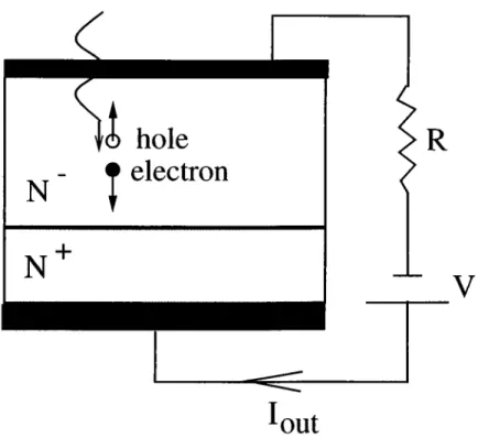
___________
hole
^ -
t electron
N
]
N-^
R
V
Iout
Figure 2.2: Photogenerated carriers inside the depletion layer
where A** is the effective Richardson constant.
2.1.2
Detector Operation
When a reverse bias is applied to the device, as shown in Figure 2.2, the voltage drop across the depletion region increases. This additional voltage drop results in a wider depletion region, and a continuous electric field across the N- region. When a photon with wavelength A, whose energy is larger than the bandgap, is absorbed in the depletion region an electron hole pair is generated. These carriers are swept away by the electric field.
The number o f electrons generated per incident photon is defined as the quantum efficiency, which is expressed as'“^:
7/
CHAPTER 2. THEORETICAL BACKGROUND
Figure 2.3: The carriers generated at a: = ,x'o induce output current as they move across the depletion region
where Ip is the photo-generated current, is the optical power at frequency /y. The depletion region can be described as a parallel plate capacitor, with area A, width d, and dielectric constant e. At steady state, the voltage across the capacitor is Vq, which results in a total charge Qo = CVq.
Let’s assume that, at time i = 0, a narrow optical pulse generates carriers with a total charge of q, at a distance Xq from the Schottky contact, as shown in
Figure 2.3. Due to the built-in electric field in the depletion layer, the positive and negative charges are pulled in opposite directions, forming charged sheets with a surface charge density a — q/A. The negatively charged sheet corresponds to electrons moving away from the Schottky contact with drift velocity Vg, and positively charged sheet corresponds to holes moving towards the Schottky contact with drift velocity 'C/,. Each sheet contributes to the electric field formed between the sheets:
i?. = - (
2.8)
£
The direction of this electric field is opposite to the depletion layer electric field, which results in a voltage drop across the depletion layer as the charges move
away from each other. This time dependent voltage is expressed as^^:
fXc(t)
/xh{t)
where these time dependent coordinates can be expressed as: r X c ( t )
Va{t) - / E^dx = E^[Xe{t) - Xh{t)] JxiAt) Xe{t) = Xo + '»et ,0 < t < te X k { t ) = X o - V h t , 0 < t < t h (2.9) (2.10) (2.11)
where tg = {d—xo)/ve and th = xq/vu are electron and hole transit time, defined as the time required for the carriers to complete their transport. Assuming te > th, we can write for the potential drop due to the carriers as:
K ,( i) =
i{Ve+Vi,)t ,
0
< i < ( , , , tfi t <C.fVet (2.12)
We can write the output current Iout{t) as:
' “ 'W = ^
where V{t) = Vq — V^{t), so the time dependent current is:
j (.\ _ ) = + W/i) , 0 < t < th ^OUtU) — \ r
h = j,Ve , t h < t < C
(2.13)
(2.14)
This time dependent expression is plotted in Figure 2.4.
We can use the same formalism to obtain the output of different cases. In one case, we assume that the absorption over the depletion layer is constant, and the hole drift velocity is smaller than the electron drift velocity, > Vh- In this case, when all the electrons reach the end of the depletion layer, there exist some holes that contribute to the total current. So the current flows until all the holes leave the depletion layer. Current output of such a device is shown on Figure 2.5. Another case is that, the absorption constant is so high that all the light is absorbed near the Schottky contact. In this case the current output is a square that continues until i«.
CHAPTER 2. THEORETICAL BACKGROUND 10
Figure 2.5: Expected output current for a uniformly illuminated diode where hole drift velocity is smaller than the electron drift velocity
2.1.3
Diode Performance
One o f the important parameter that reflects the performance of a photodetector is the quantum efficiency, rj. For classical photodetectors the expression for the quantum efficiency is given by,
r ;= ( 1 - i ? , ) ( l (2. 15)
where R is the reflectivity of the front surface, a is the power absorption coefficient and d is the thickness of the absorbing layer. So to maximize the quantum efficiency, the surface reflectivity must be minimized, and single pass absorption must be maximized. Reflectivity can be minimized using anti-reflection coatings, and single pass absorption can be maximized by increasing layer thickness.
Another important characteristic is the bandwidth (speed) of the photodiode. The speed is limited by two factors, transit time of the carriers, and the RC time constant of the photodiode.
High frequency analysis can be carried out using the the circuit model in Figure
2.6(b). The photodiode can be modeled by a parallel combination of a
current source Ip{t), and a capacitor C,i that represents the capacitance due to the depletion layer. The series resistance of the diode is much smaller than the load impedance, and is not included in the model.For the transit time limited case, the 3-dB roll-off frequency can be expressed as:
(2.16) fir = 0 .4 5 ^
For the RC constant limited case, the 3-dB roll-off frequency is:
1
fliC —
77
(2.17)‘I'nRiCd
The well-known bandwidth-efficiency trade-off is the major blockade for using high speed photodiodes in long-haul telecommunications. As the active layer thickness decreases to minimize the transit time for high speed operation, the quantum efficiency of the same device decreases. For thin active layers, the absorption can be formulated as
CHAPTER 2. THEORETICAL BACKGROUND 12
Rb
photodiode
(b)
Figure 2.6: (a)Schematics of the photodiode circuitry (l))E(iuivalent circuit model for high frequency analysis
Figure 2.7; Excitation of eri electron in the internal pliotoemission
where ad <C 1 is assumed. Then the bandwidth-efficiency product for a transit time limited photodetector can be obtained as,
(2.19) fir ■ V ~ b.45(l — R) Vf,a
which is independent of of the active layer thickness.
2.2
Internal Photoemission
Schottky diodes are becoming increasingly popular as infrared detectors, despite their low quantum efficiencies relative to other infrared detectors. This is because large format Schottky diode arrays can be fabricated using the same processing procedure as the other integrated circuitry. Iridium silicide Schottky barrier diodes with a cut-off wavelength of more than
10 /irn have been demonstrated.'''
Internal photoemission corresponds to the optical excitation of electrons in the metal to an energy above the Schottky barrier and then transport to the conduction band of the semiconductor which is shown in Figure 2.7. According to
CHAPTER 2. THEORETICAL BACKGROUND 14
the theory developed by Fowler, the number of electrons emitted per quantum of light absorbed is to a first approximation proportional to the number of electrons per unit volume of the metal whose kinetic energy normal to the surface is sufficient to overcome the potential step of the surface. We may call the number the number of available electrons.
In a gas o f electrons obeying the Ferrni-Dirac statistics, the number of electrons per unit volume having velocity component in the range u + du, v + dv, w + dw is given l)y the formula:
, N
7
, , ^ dudvdwn[u, V, w)dudvdw = 2 1
-V h J ^[^m{u^+v'^+w'^)-Ep]/kT _j_ ^ (2.20) The number of electrons per unit volume n{u)du with velocity component normal to the surface in the range u, u + du is given by:
j pdpdO
— ] d u / -
77
-h J Jo Jo A r (2.21)
(
2.
22)
when the integral is taken, we end with an expression:
n{u)du = + l]du
m \ h J
As explained before, only the electrons with a total kinetic energy (after absorbing the photon with energy hi/) normal to the interface is larger than Ej,' + (¡)b can go over the Schottky barrier and contribute to the photocurrent. The number of available electrons is given by:
/•00
N = n{u)du
J\rmP=Ep+<p}i—lw (2.23)
where n{u)du is given by Eq.(2.20). By making a change of variable y — {hi' — 4>B — Eb + Rmu^)/kT , we obtain:
^ 2TrkT / 2 7 r h T V ' ^ ^ r m V rn ) V li J Jo
log[l + .7]
d.y (2.24) m y rn J V h J Jo [y + [Eb + (¡)b — hn)/kT]
To simplify this integral, we consider the region hu near (///^ Then, it is a good approximation to neglect y in the denominator of the integral, therefore,
2s/2 rmP^'^ikT)'^ foo N
(a) When
7 =
{hi/ — 4>B)/kT <0, the logarithmic term can be expanded, and
integrated term by term. ThenN = 2^/2 7rm^/2 { k T f
1/2
(/¿7
g37( 7 < 0 ) (2.26)
(b) When
7 =
{hu — (¡)B)/kT > 0, the logarithmic term can be expanded, and integrated term by term, givingr o o / log[l +
0
Jo 2-27
p-37 e“ - “ 22 32 (2.27) So: N 2V2 { k T f 7--- h t2 - 71
2
6 2 ^ A.-'l' p-27 CJ-37
+ ' 22 32 (7 > 0) (2.28) We are interested in the situation7 >
0. Above threshold, for
7 >
6
our expression takes the formN = AT'^^^ (2.29)
with an accuracy of 5%.^^’ We can assume that the photoelectric current / per quantum of light absorbed is proportional to N. So for quantum efficiency, we can write:
{hi/ - (¡)bY , {hu > (¡)b)
0
, {hu < (¡)b)We derived Eq. 2.30 for bulk material, and didn’t take into account the thickness of the Schottky layer. When the reflections from the walls of the metal are taken into account, it has been found that there is an enhancement in the quantum efficiency, but the dependence on the wavelength of the photons is the
r] oc (2.30)
same 1 7 - 1 9
2.3
Resonant Cavity Enhancement
For transit time limited photodetectors, the depletion region must be kept thin for the high speed operation. On the other hand, for high quantum efficiency
CHAPTER 2. THEORETICAL BACKGROUND 16
Absorption
Region
the depletion layer must be sufficiently thick to absorb a high fraction of incident light. To overcome this trade off between the response speed and efficiency, we can place a conventional photodetector with a thinner active layer inside a Fabry-Perot rnicrocavity. Thinner active layer results in lower transit time, which increases the performance of the photodetector. This kind of enhancement of the quantum efficiency is called Resonant Cavity Enhancement (RCE). RCE effect was proposoid in 1990 and was applied to a broad range of detectors: Schottky, p-i-n,^‘ and avalanche'·^'*photodiodes.
2.3.1
RCE Formulation
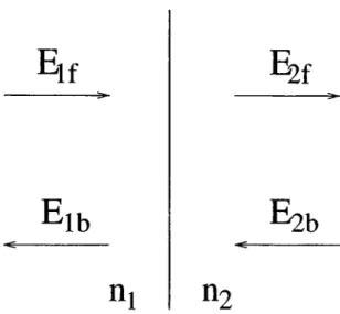
Figure 2.8 shows a generalized structure of an RCE photodetector. As the aim is to achieve maximum efficiency, lossless distributed Bragg reflectors (DBR) are used as mirrors of the microcavity. Active layer, where the absorption occurs, is placed between these mirrors. L is the length of the cavity and d is the thickness of the active layer. The field reflection coefficient of the top and bottom reflectors are and r2e*‘^'C where and <p2 are phase shifts due to the light penetration into the mirrors. Ej represents the electric field amplitude of the incident light, while E / is the forward traveling wave at 2 = 0, and E;, is the backward traveling wave 'dt z —L. In the cavity, Ey is composed of the transmitted wave from the first mirrors and the reflected wave from the second mirror. Therefore the forward traveling wave, Ey, at
2
; = 0 can be obtained in a self-consistent way:f (2.31)
where /i = 27rn/Ao, a and cVgx are the absorption eoefficients of the active and cavity layers respectively. Solving for Ey gives us
L
E f = -E,
and backward traveling wave, E^, dt z = L can be expressed as.
(2.32)
(2.33)
The optical power inside the resonant cavity is proportional to the refractive index of the medium and the square of the electric field amplitude.
P{z) (X \E{z)\'^n (2..34)
where E{z) = Ej-{z) + Et,{z) is the total electric field. Neglecting the standing wave effect, the power absorbed in the active layer is given by:
Pi
1 - 2r
/ V ________________ Z________________________/_\_________________ / p
rir2( r ‘^^'^ cos(2/iL + (/;| + f/>
2
) + (r]r2)‘‘^e~·-^“ '·^'CHAPTER 2. THEORETICAL BACKGROUND 18
where «c = ( < ^ e x { L i + L2) + ad)/L. Under the assumption that all the photogen erated carriers contribute to the current, rj is the ratio of the absorbed power to the incident optical power, i.e., rj — Pi/Pi- Hence:
V
1 — 2^/R/R^e~°‘<=^ cos{2/3L +
(/>1
-I- (/>2
)-I-(2.36) While designing the detector, the cavity layers are chosen such that all the light is absorbed in the active layer («^3,· “C a). The expression in the square braces is call the enhancement, as it is the multiplier to the quantum efficiency of a conventional photodiode. Enhancement can be rewritten as:
(1
enhancement — (2.37)
1
— 2-\/R1R2 e cos{2PL -h (f>i -I- <¡(>2
) -h R1R2 eFrom this expression, it is seen that rj is enhanced periodically at the resonant wavelengths of the cavity, 2^L- f - </»]-1-(/^2 = 2mTr (m = 1, 2,3...). This term introduces the wavelength selectivity of the RCE effect.
2.3.2
Standing Wave Effect
While deriving Eq.(2.37), the spatial distribution of the optical field inside the cavity was neglected. This spatial distribution arises from the standing wave formed by the two counter propagating waves. This is referred as standing wave effect (SWE).
The SWE is conveniently included in the formalism of rj as an effective absorption constant, i.e., cvejf = S W E x a. The effective absorption constant «e/y is the normalized integral of a and the field intensity across the absorption region.
_ i/;f a :( z ) |E(z,A)p dz
cy.(} f f — » 1,^
\E(z,\)P dz
When detectors with thick active layers which span several periods of the standing wave arc considered, SWE can be neglected. For very thin active layers, which are necessary for strained layer absorbers, SWE must be considered.
( ad=0.1, R,=99.99% )
Top Mirror Reflectivity R, (%)
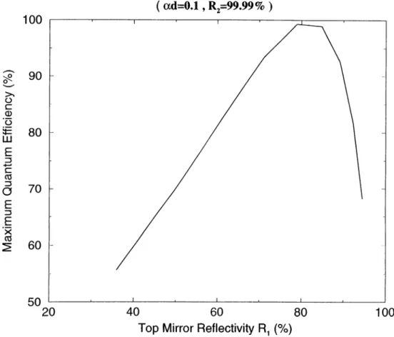
Figure 2.9: QE for different top DBR reflectivities (R i) for ad — 0.1 and R,2 99.99%
2.3.3
RCE Optimization
From the expression for the quantum efficiency (r/), we see that three parameters Ri, R,2, and ad effects rj. R2, the reflectivity of the bottom mirror, should be designed as high as possible. Else, due to the transmission from the bottom mirror, the performance of the detector decreases dramatically. The other parameter is the reflectivity of the top mirror. When we maximize the quantum efficiency with respect to R i, we come up with the condition:
CHAPTER 2. THEORETICAL BACKGROUND 20
700 750 800
Wavelength (nm)
850 900
Figure
2.10: QE spectrum for different top DBR reflectivities (R|) for
ad =0.1
and R2
= 99.99%( R ,= 78.9% , R2=99.9% )
Figure
2.11: QE spectrum for different
ad with DBR reflectivities Ri = 78.9% and R2 = 99.99%CHAPTER 2. THEORETICAL BACKGROUND 22
The structure used in the simulations consists of 5 pair AlAs/air bottom DBR with a reflectivity of R2 = 99.99% at 800 nm and cavity is formed with 950 rirn semiconductor with refractive index of 4. Active layer is placed in the center of the layer with ad = 0.1. Top DBR consists of Si:iN^/Si02 pairs with a center wavelength Ac =800 nm. As we increase R| by increasing the number of SiiN\/SiOz pairs up to the matching value, Ri = 0.81, the peak quantum efficiency value increases up to 99%, then decreases as shown in Figure 2.9. Figure 2.10 shows the quantum efficiency spectrum, where the full width at half maximum (FWHM) decreases as Ri increases and the shift in the resonance wavelengths around 740 and 860 nm is due to the penetration of light into the DBR.
Other important parameter for RCE is ad. We simulated for different ad values with Ri = 79.0% and R
2
= 99.9% and the results are presented in Figure 2.11. When ad increases the effect of RCE hence wavelength selectivity, decreases as all the light is absorbed in a single pass without recycling in the cavity.Design
In the past 10 years, detector technology has seen a dramatic increase parallel to epitaxial growth technology. New detector materials and structures as well as more complex architectures have become possible to grow. Optical frequencies cover a wide spectrum, from extreme ultraviolet (EUV, ~
10nm) to far infrared
(FIR, >12/iim). Each spectrum portion has its own applications. UV is used
for combustion monitoring, satellite-based missile plume detection, air quality sensing and gas sensing.^® Visible spectrum is used for display, optical storage, and short distance fiber communication. Near infrared contains 1.3 and 1.55 /rrn, which are the second and third fiber communication windows used for long distance communication.'^^ IR is used for military applications, remote sensing, gas detection and medical applications.3.1
Materials for Photodetectors
The performance of an optical communication system is measured with its l)andwidth/cost ratio. To increase this ratio, there is a demand for high l)erforrnance components, like hbers, lasers, modulators, filters and detectors. It is known that R.CE photodiodes offer high-performance with high quantum efficiencies. Features for a proper material system of RCE-detection are very important for a good design:
CHAPTERS. DESIGN 24
• Low-loss cavity is very important for limiting the absorption to the active layer
• High-reflectance bottom mirror (DBR) designed with non-absorbing mate rials increases both quantum efficiency and quality factor of the cavity • Moderate active layer absorption, ad
• Lattice matched materials must be used to be free from defects Different material systems can be summarized as below:
• G a N /Z n S T e : These materials operate in UV and GaN has many advantages over Si, SiC and Ge which can operate in this wavelength region, but lags in development. GaN, ZnSTe and other nitride based materials eg. AIN, InN are direct bandgap, and they are most promising materials for light-emitting devices in the blue, violet, and ultraviolet region. GaN p-TT-n^^, Schottky and pn junction photodetectors can be grown on Si,'*^ and sa p ph ire,w h erea s high-efficiency ZnSTe photodetectors can be grown on Si, GaAs and GaP.^^
• A l A s /A l G a A s /G a A s : These materials are grown by MBE very easily, since there is a good lattice match between them. Growth of Al;cGai_xAs ternary materials enable designs containing graded layers. Since GaAs with a bandgap of 870 nrn is used as the active layer, such detectors are used for the first optical communication window. Low-loss or no-loss cavity formation is possible with ARGai-^As cavity layers and ARGai_,KAs/AlAs pairs for bottom DBR. Unfortunately large number of pairs must be used to get nearly unity reflectivity due to the low refractive index difference of these materials.
• A lG a A s /G a A s /I n G a A s : IriGaAs is used as the active layer in this material system. AlAs has a good lattice match to GaAs, and G aA s/A lA s mirrors can function easily at 1.55 //in. But it is not easy to grow Iri;,;Gai_,cAs layers on top of Al,;Gai_.,,.As due to lattice mismatch. Hence
it is not possible to make a photodiode operating at 1.3 /mi and 1.55 /xm with this material system. But high-performance RCE photodiodes have been demonstrated at 900 nm.’^*^’^^
I n P /I n G a A s /I n A l A s : When InP used as substrate, the Ino.53Gao.47As/Ino.52Alo.48As system grows lattice matched, and their electrical properties and ability to operate between 1.3 /mi and 1.55 /mi makes them most appropriate materials in this region. One disadvantage is the poor refractive index contrast between InGaAs and InAlAs. To overcome this GaAs/AlAs mirrors can be wafer-fused to form the microcavity.
S i/G e : Operation region starts from UV, and extend their range to visible. Ge can operate up to
1.8
/xm. Wide band-gap silicon carbide (SiC) with advanced stage of development seems to be the most suitable material for high-temperature, high-power devices. Si/SiGe DBR for Si and A lA s/G aA s DBR for Ge can be used. The only disadvantage of these materials is that they are indirect bandgap materials.H g x Z n i_3;T e /I n S b /I n A s : These materials can operate in the IR region. HgZriTe has been grown in mid 80’s, but its growth difficulty has limited its applicability. But in 90’s IriTlSb has been grown successfully. At these wavelength HgGdTe is still dominant because of its advanced growth technology. By changing Hg concentration in Hg,cZni_,:Te, detection can be extended beyond 15 ^rn.
3.2
Device Simulation
Our detector designs, like other RCE photodetectors and VCSELs, are quite complicated and difficult -also very expensive- to grow. Optical properties of materials used in the growth aixi wavehingth dependent and this makes rather difficult to predict the optical field in such multilayer devices, therefore we need
CHAPTERS. DESIGN 26 ^ If
'lb
» 1
» 2E
^ 2 5
Figure 3.1: Electric fields at the interface
a good simulation method for the analysis before ordering the structure for MBE growth. We used transfer matrix method (TM M ), which provides a simple technique to calculate electric and magnetic field distributions inside the cavity.
When we model a layer from an optical point of view, we notice that it consists of two elements; an interface where an abrupt refractive index difference occurs, and a slab where refractive index is constant and extends for a certain width. Refractive index is defined as the square root of the dielectric constant of the medium ; n = \/e — ii. Imaginary part of the dielectric constant is due to the absorption in the medium, and refractive index can be simplified as n = Ureal ~ '^kmagi wliere both Ureal 'fHrTiag are real and positive iiumbers.
Electric fields at the left and right of the interface as defined in Figure 3.1 can be related to each other using continuity of the electric and magnetic fields, and given as:
P j l c 1 I r 1 E j n r
(3,1)
1 1 r \ E 2] ·
E \ b 1 E 2I )
n
1
X ^2b
H2 E i f ( x ) E i b W AFigure 3.2: Electric field inside a layer
the layer (Figure 3.2) can be found by using the propagation of plane wave:
E2f{x) ^—ikx 0 E2f
_ E2b{x) _ 0 ^jikx E2b
(3.2)
where k = (27m )/A . When we choose x to be equal to the width of the layer, we can evaluate the electric field just at the left of the next interface. So combining- two matrices used in Eq.(3.1) and Eq.(3.2), we can define a transfer matrix for mth layer as:
5 - J _
^TTl -- . Truen—iS· (3.3)
e
where + = (2iifn.)/(n.,7i +
77
/„i.|,^), and 5jji — kjfidjji. Cascading these matrices for N layers, total transfer matrix for the multilayer system is constructed as:Stotal — SqSi · · · N (3.4)
So the relation between the electric field at the left and at the right sides of our system as depicted in Figure 3.3 is given by:
Ehf Ehb
= Stotal Eaf
Eab
CHAPTERS. DESIGN 28
Figure 3.3: Electric fields outside our structure
When we make a measurement like reflectivity, we measure the reflected power not the electric field. The same is valid for the transmittivity and absorption. We can find the power associated with a plane wave using
and using S = - E x B /i B ^ - k x E ÜÜ (3.6) (3.7) we find that the power is proportional to the square of the electric field and the refractive index of the medium. Then the reflectivity and the transmittivity are given by: R = T = \Eibb \E,ff f İn a l
I / I
'^Hncidence (3.8) (3.9) Absorption at any layer is found by finding the difference between the power getting into the medium and the power getting out of the medium.3.3
Cavity Design
As shown in the previous chapter, our aim is to place the active layer inside a cavity formed by two mirrors. Our designs require bottom mirrors with high
Bottom D B R of ISU S am ple 1 10 0 1 20 0 1 300 1 400 1500 W avelength (nm) Bottom D B R of N IS T S am p le 7 5 0 8 00 8 5 0 9 0 0 9 5 0 W avelength (nm )
Figure 3.4: Reflectivity of DBRs used in NIST and ISU samples
reflectivities. Although metals are good reflectors, their reflectivities (R < 96 for thick layers) are not high enough, and change with the spectrum. One of the main disadvantages of metal mirrors is that they are good absorbers at the optical wavelengths, so very thin layers must be used.
Distributed Bragg reflectors (D BR’s) are widely used in optoelectronic applications such as detectors and semiconductor lasers. A DBR is a periodic stack with two alternating quarter-wave thick materials with different optical properties. Each pair consist of two layers with refractive indices ni and 112, and layer thicknesses of X j^ n] and A^/4n2 respectively. A,, is the central wavelength of the mirror where reflectivity is maximum.
When we observe the light reflected from different interfaces of one pair, we see that all are at the same phase resulting in a constructive interference hence increasing the reflectivity. Applying TMM for a DBR at center wavelength A,;, results in a simple expression for the reflectivity as
R-max
n2N m2N'
nM + 2N r4, 2N (3.10)
CHAPTERS. DESIGN 30
reflectance approaches unity, and for a fixed N reflectivity increases as n2/n i increases. %99.6 reflectivity has been achieved with only 2.5 pairs of InP /A ir DBR, where as the same reflectivity can be achieved with 51 pair InGaAsP/InP DBR.^® SÍ/SÍO2 is another material system that can be used with Si based devices.
With a small change in the design of the DBRs, the nature of these mirrors can be changed. If the width of one of the layers (with a refractive index of ni) increased from A,./4ni to Xcf2rii, the structure becomes transparent around while still reflecting other wavelengths. In this case, the multilayer stack functions as a filter. Such filters have been demonstrated at various wavelengths on both silicon and GaAs based devices.
3 . 4
NIST Sample
This sample is grown in the National Institute of Standard and Technology (NIST) by molecular beam epitaxy (MBE) technique. Epitaxial design of NIST sample is shown in Figure 3.5.
3.4.1 Design and Optimization
Although semitransparent gold Schottky contact is a good top mirror, it absorbs and scatters a large fraction of light. Instead of metals, indium tin oxide (ITO), cadmium tin oxide (CTO) have been studied as Schottky material for MSM devices, photodetectors, LEDs, and solar c e l l s . I n fact ITO is a highly degenerate n-type semiconductor, that has electrical resistivity of 2-4xlO “ '‘ Ocm.‘^^ ITO is a wide gap material (3.3-3.4 eV) that shows high transmission in the visible and near-IR, regions of the spectrum. Electrical, optical and structural properties of this material strongly depend on the deposition conditions. We grow ITO layer using magnetron sputtering in the Ar plasma. Our ellipsorneter measurements of ITO yielded a refractive index of 2.0, which is in good agreement with the values reported in literature. Several deposition techniques have been used to grow ITO films including chemical
80 nm A l Q j ^ a Q g g A s N -30 nm Graded Region N -120 nm GaAs N-30 nm Graded Region N~ 160 nm A1Q 2G a q gAs N -400 nm A1Q 2G a q gAs N +
230 nm A1Q q gAs Undoped
100 nm Alf^^Gaf^gAs
N-19 pair A1Q 2^^o 8^^ /A lA s D B R
CHAPTERS. DESIGN 32
vapor deposition, magnetron sputtering, evaporation and pulsed laser deposition (PLD). According to the atomic force microscopy measurements, root-mean- square surface roughness of magnetron sputtered films is ~40 Angstroms where PLD films is <^5 Angstroms.
The design wavelength of NIST photodiode is 840 nrn, so that it can operate in the first optical communication window. GaAs is used as the active layer, and the thickness is chosen to be
120
run, which the half wavelength of the resonance wavelength. When the standing wave effect (SWE) is taken into account, the position of the active layer is not important in this case. Hence, we can make wavelength tuning before the fabrication.In order to have a low-loss cavity, Alo.15Gao.85As and Alo.20Gao.80As are used for immediate cavity materials. Bottom mirror consists of 19 period AlAs/Alo.2Gao.8As Bragg mirror designed at 840 nm. 230 nrn thick Alo.2Gao.3As undoped layer is for the mesa isolation. Sharp interfaces cause carrier trapping problems at the interfaces, and graded regions are used to get rid of this problem.
100 nm ITO layer is used as the Schottky layer. To achieve the maximum
(luantum efficiency, 5 pair Si3N4/S i()2 DBR must be deposited as the top mirror.
As another design criteria, electron and hole drift velocities are taken into account. Absorption layer is placed closer to the Schottky contact, and the hole and electron transit lengths are chosen such that the electron and hole transit times are equalized (¿e = t/,.).
3.4.2
Reflectivity Characterization
Before the fabrication, we measured the reflectivity of the sample. We can deduce useful information about the epitaxial striicture of the sample by comparing the reflectivity measurements with the theoretical predictions. After the reflectivity measurements, we found out that there was a
1
% deviation from the original epilayer design. By changing the simulation parameter, we made a fit to reflectivity data, that is shown in Figure 3.C with the reflectivity measurement.W avelength (nm)
Figure 3.6: Measured (solid line) and simulated (dotted line) reflectivity of NIST sample
CHAPTERS. DESIGN 34 2 0 0 nm G aA s N -6 0 0 nm G aA s N + 3 0 0 nm G aA s U ndoped 15 pair A lA s/G a A s D B R Sem i-Insulating G aA s
Figure 3.7; Epitaxial design of ISU sample
had to bias the diode to 6 V to deplete the n- layers. Before fabricating with ITO Schottky layer, we decided to recess etch the sample until the n- GaAs layer, to deplete the n- layers at a lower bias.
3.5
ISU Sample
This sample is grown in Iowa State University (ISU) by molecular beam epitaxy (MBE) technique. Epitaxial design of the ISU sample is shown in Figure 3.7.
3.5.1 Design and Optimization
This photodiode is designed to operate at 1.3 /im, so that it can be used for the 2"^^ optical communication window. It consists of GaAs layers as cavity layers, n- layer is very lightly doped, and n+ region is doped to 10^*^ cm “ ^ for the ohmic contact. Bottom mirror consists of 15 pair AlAs/GaAs DBR centered at 1.3 fun. This mirror has reflectivity greater than 95% between 1244 nm and 1359 nrri. Maximum reflectivity of 99% is achieved at 1300nm.
The photons will be absorbed at the gold Schottky layer, and the photo generated electrons which can travel over the Schottky barrier to the depletion
Wavelength (nm)
Figure 3.8: Measured (solid line) and simulated (dotted line) reflectivity of ISU sample
layer will be detected. The Au-Scliottky barrier has barrier height of
0.8 eV.
So signals up to 1.5 /urn should be detected according to the theory of internal photoemission.The resonant wavelength of the designed cavity is 1.4 //rn. By etching the top GaAs layer, the resonant wavelength can be tuned to the desired value of 1.3 pin.
3.5.2
Reflectivity Characterization
Before the fabrication, we measured the ndiectivity spectrum of the sample. We fitted the simulation to the reflectivity data by changing the thickness of the layers in the simulation. We found out that there was a 4-6% deviation from the
CHAPTERS. DESIGN 36
Figure 3.9: Crosssection of ISU sample taken with SEM
original epilayer design. Due to this deviation, the center of the mirror has shifted to 1.37 //rn. Figure 3.8 shows the measured and simulated reflectivity spectrum. Figure 3.9 shows the crossection of the ISU sample obtained by scanning electron microscopy (SEM). The DBR layers of the ISU sample can be seen as lines with different colors.
The lower edge of the DBR mirror starts an 1.3 /mi. We decided to shift the resonance to 1.33 /¿rri, by etching 50 nm GaAs layer from the top. Our simulations predict that the resonance wavelength should shift to 1.31 /mi after the deposition of the Schottky gold metal.
Fabrication
Fabrication of high speed photodiodes consists of many steps, some of which are very important for high speed operation, like airpost, bridge and top DBR deposition. Airpost and bridge steps are introduced to decrease parasitic capacitance of the device and fabrication of metal-insulater-metal (MIM) capacitor. Top DBR deposition is due to the requirements of the RCE effect. With these steps, our fabrication process consists of eight steps, some of which involves two or more photolithography. Fortunately, most of the high speed photodetector fabrication process steps have already been developed by previous and present graduate students of our laboratory. We developed Schottky contact formation to A ^ G a i-jA s with indium-tin-oxide (ITO). We also deposited the SÍO2/S Í3N4 top dielectric mirror to be used as a part of the RCE photodetector. All of the fabrication processes are made in our Advanced Research Laboratories in a Class-100 clean room environment.
4.1
Standard Processes
4.1.1
Cleaving and Wafer Cleaning
We prefer working with small samples cleaved from very expensive MBE grown wafers. Sample sizes are around
8x
8
mm and the mask is 7 x 7 mm square. WeCHAPTER 4. FABRICATION 38
use a diamond tipped scriber-pen to define a line at the back of the substrate. After defining the shape of the sample, the wafer can be easily cleaved.
Every step starts with a standard cleaning process, called three solvent cleaning (TSC). Samples are immersed into the boiling trichloroethane for
2
minutes, then to acetone at room temperature for 5 minutes, and finally to boiling isopropanol for2
minutes. Trichloroethane dissolves any possible oils, acetone dissolves organic molecules, photoresist residues and trichloroethane, and isopropanol dissolves acetone. Samples are rinsed in the deionized (DI) water flow and dried with nitrogen gun. Cleaning ends with dehydration bake at120 °C for
2
minutes on a hot plate.4.1.2
Photolithography
Photolithography (PL) is the name of patterning the features on to the surface o f the sample. These patterning techniques involve energy-sensitive chemical substances called resist. The exposure can be done using ultraviolet (UV) light, electron beam, x-ray etc. according to the resist used. We use AZ5214E type resist which has an absorption peak around 360 nm that is ideal for UV exposure with Hg (i-line at 365 nm) lamb. Alignment is achieved by using a Karl-Suss MJB3 mask aligner.
The sample surface is first covered with an adhesion-promoter called HMDS, which provides a better adhesion of the photoresist to the surface o f the sample. Then, the resist is applied on the surface. Both HMDS and resist are spun at 5000 RPM. The resultant resist thickness is around 1.3 /irn. The samples are then baked at
110 °C for 55 seconds. At this point, we choose one of the following PL
methods.• Normal Photolithography : After pre-bake, the sample is aligned with respect to the mask. The sample is then exposed under UV-larnp for about 26 seconds with an optical power of 5.0 rnW /cnP for a total dose o f 130 mJ/crrP.
Resisr
Semiconductor Substrate
Resist
Semiconductor Substrate
Normal PL
Image-reversal PL
Figure 4.1: Resist profile of normal and image-reversal photolithography
aligned with respect to the image reversal mask. The sample is then exposed under UV-lamp for about 10 seconds with an optical power of 5.0 rnW/cm'^ for a total dose of 50 m J/cnF. Then the sample is baked at
110 °C for
2
minutes. After the bake, the whole sample is exposed for 30 seconds with an optical power of 5.0 m W /cm ‘^ for a total dose of 150 rnJ/crrF.For the development of the exposed samples, AZ400K developer is used with a 1:4 (Developer:H20) ratio. As the desired regions of the resist are etched by the developer, change in the color can be observed with naked eye. When this color change stops, sample is rinsed under DI water. After drying the sample, we check the alignment and the development. The resolution patterns must be sharp, and for a good photolithography ~ l/im resolution should be observable. Image reversal PL helps a lot for overcoming the lift-off problem of thick metalization. Normal PL is used for thin metalization, etch, and post step.
4.1.3
Etching
Etching is used for transforming the defined patterns by PL onto the underlying metal, semiconductor or dielectric layers, so that the desired layer is reached for the subsequent process. Etching is also used for cleaning resist, removing damaged material, polishing, removing surface oxides. Two types o f etching is used in the semiconductor processes: wet and dry etching.
• W et Etching : Chemical reactions that occur at the surface of the material are the main mechanisms for the wet etch. The etch mechanism of GaAs
CHAPTER. 4. FABB.ICATION 40
Figure 4.2; SEM image of wet-etch profile
based semiconductors, is first to oxidize the surface with an oxidizing agent, and then remove the oxidized layer with acid or base. Many etchants have been reported for etching GaAs.'*'‘ In fact any oxidizer and oxide- dissolver combination will act as etchant. Some of them has gained pop ularity in the GaAs process, such as; H2SO4-H2O2-H2O, HCI-H2O2-H2O, HGl-GH3G0 0H-K2Gr207, Br-CHaOH.^^ Dielectric materials such as SiOa, Si.3N4, T i02, AI2O3 can be etched using hydrofluoric acid (HF), buffered HF, or phosphoric acid (H3PO