Evgeniya Kovalska,
*
Ihor Pavlov,
Petro Deminskyi,
Anna Baldycheva,
F. Ömer Ilday,
and Coskun Kocabas
†,∥†Laboratory of Smart Materials and Devices, Department of Physics, and§Ultrafast Optics and Lasers Laboratory, Department of Physics, Bilkent University, Ankara 06800, Turkey
‡Department of Engineering and Centre for Graphene Science, College of Engineering, Mathematics and Physical Sciences, University of Exeter, Exeter EX4 4QF, U.K.
∥Materials Science Center, School of Materials, University of Manchester, Oxford Rd., Manchester M13 9PL, U.K.
*
S Supporting InformationABSTRACT: The range of applications of diverse graphene-based devices could be limited by insufficient surface reactivity, unsatisfied shaping, or null energy gap of graphene. Engineering the graphene structure by laser techniques can adjust the transport properties and the surface area of graphene, providing devices of different nature with a higher capacitance. Additionally, the created periodic potential and appearance of the active external/inner/edge surface centers determine the multifunction-ality of the graphene surface and corresponding devices. Here, we report on thefirst implementation of nonlinear laser lithography (NLL) for multilayer graphene (MLG) structuring, which offers a low-cost, single-step, and high-speed nanofabrication process. The NLL relies on the employment of a high repetition rate femtosecond Yb fiber laser that provides generation of highly
reproducible, robust, uniform, and periodic nanostructures over a large surface area (1 cm2/15 s). NLL allows one to obtain
clearly predesigned patterned graphene structures without fabrication tolerances, which are caused by contacting mask contamination, polymer residuals, and direct laser exposure of the graphene layers. We represent regularly patterned MLG (p-MLG) obtained by the chemical vapor deposition method on an NLL-structured Ni foil. We also demonstrate tuning of chemical (wettability) and electro-optical (transmittance and sheet resistance) properties of p-MLG by laser power adjustments. In conclusion, we show the great promise of fabricated devices, namely, supercapacitors, and Li-ion batteries by using NLL-assisted graphene patterning. Our approach demonstrates a new avenue to pattern graphene for multifunctional device engineering in optics, photonics, and bioelectronics.
■
INTRODUCTIONThe patterning and microstructuring of graphene films can selectively enhance certain (opto)electronic capabilities of graphene-based devices and can offer not only new applications but also most importantly multifunctionality of the next generation graphene-based devices for energy storage, photonics, and bioelectronics.1−4 Engineering graphene structure restricts the motion of electrons in specific directions, for example, by forming a junction-like structure that changes from a zero-gap conductor to a semiconductor. Hence, when graphene is patterned into narrow ribbons5 or ordered in accordance with the substrate geometry,6 we expect the opening of an energy gap and, consequently, tuning of the transport properties of graphene-based devices. Besides, patterning increases the specific surface area of graphene, which resulted in a higher capacity of corresponding devices. The multifunctionality of the graphene surface driven by imposing a super periodic potential7and forming active centers (by defects, oxygen-based functional groups, and self-assembled
monolayers) controls graphene electronic properties consis-tently. Therefore, patterning of graphene could be a good approach for tuning the transport properties of graphene-based devices and the reactivity by increasing the surface area and artificial ordering of graphene.
Several methods which require execution of different steps for the patterning procedure have been demonstrated. For example, mechanical cleavage,8 scanning probe lithography,9 photocatalytic etching,10 plasma etching,11 chemical etch-ing,11,12 assembling,13 combination of soft-lithography with oxygen plasma etching,14,15 and so forth. Although these methods are suitable for large-scale fabrication of a variety of patterns, they involve multiple processes and, therefore, are time consuming and costly. Alternatively, so-called in situ techniques enable the growth of already-patterned structure Received: November 25, 2017
Accepted: January 17, 2018 Published: February 6, 2018
based on, for example, patterning of catalytic metalfilms before growth,16 laser-induced chemical vapor deposition (CVD)17 and so forth. However, most of the grown materials require to be transferred on a desired substrate that will lead to the generation of surface and edge defects. To prevent disordered carbon−carbon bonds from film defects and to avoid the formation of contaminations (e.g., graphene release with catalyst), direct writing18,19 or cutting of already grown graphene20,21 has been employed. Among all manufacturing techniques, only nonlinear laser lithography (NLL)22a new laser-based techniqueis a single-step, high-speed (1 cm2/15 s), highly productive (does not require specified environmental conditions) and, hence, the most efficient method to fabricate small-/large-scale and mask-free micro-/nanopatterns of various nature and symmetries. Since 1965, the fabrication of regular nanostructures23 on various surfaces (metals,24 semi-conductors,25 and glasses26) was realized by laser-induced periodic surface structuringLIPSS.27 The main challenge is still precise quality control.26We propose the NLL (improved LIPSS) as a novel solution, which offers highly accurate control of the formation of nanostructures induced by ultrashort pulses. NLL initiates and regulates the metal-oxide nanostructures with unprecedented uniformity because of the positive nonlocal and negative local feedback mechanisms, respectively.22 Most importantly, a significant advantage of the method is an ability to use nonplanar/3D and rough substrate surfaces that are in demand in device engineering. In this study, we report a new approach for multilayer-graphene patterning with the NLL technique for developing high-resolution graphene-based microstructured devices on various substrates.
We experimentally demonstrate the feasibility of predeter-mined patterning of multilayer graphene (p-MLG) on a nickel substrate by using a high-power femtosecond (FS) Yb fiber laser. Regularly patterned MLG is CVD grown on the surface of preliminarily structured nickel foil, followed by transfer onto the desired substrate for characterization and device testing. The fabricated p-MLGfilms show high-quality morphology in comparison to the other existing fabrication methods, which is demonstrated by scanning electron microscopy (SEM), water contact angle (WCA) measurement, surface free energy and adhesion calculation, Raman spectroscopy, and Fourier-trans-form infrared spectroscopy. We manifest electro-optical measurements on p-MLG as well as show the performance of graphene-based devices in supercapacitor and battery con-structions. This research provides a new approach for thefirst patterning of MLG with the NLL technique for developing graphene-based devices.
■
RESULTS AND DISCUSSIONLine nanostructure formation on MLG is performed through its growth on a prepatterned nickel foil with precisely determined nanostructures on its surface. A schematic of the nano-structuring setup and the principle of the laser beam scanning over the substrate are illustrated in Figure 1a,b, respectively. Detailed characterization of the NLL technique is described in theMethod Summarypart.
Following the nickel foil surface nanostructuring, the growth of the MLGfilm is performed (Figure 2). To achieve desirable patterns, an NLL technique with coordinated adjustment of laser power (380−310 mW), a scanning speed of 1000 mm/s,
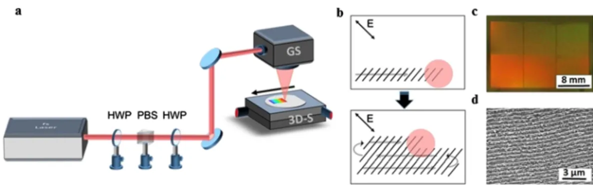
Figure 1.(a) Schematic image of a FS laser system (Yb-dopedfiber laser, 1030 nm), galvanometer scanner (GS), motorized 3D translation stage (3D-S), half-wave plate (HWP), and polarization beam splitter (PBS). (b) Scanning direction of the laser beam over the sample. The laser beam spot is represented as a pink circle. The polarization direction is indicated by an E vector. (c) Digital photograph and (d) SEM image of the structured Ni foil.
Figure 2.Schematic image of“step-by-step” patterning of graphene. (a) Nickel foil and (b) preliminary-structured nickel foil with NLL technique applying various laser power (380−310 mW). (c) CVD-grown patterned MLG on the structured nickel foil. (d) Patterning of MLG transferred onto the glass. (e) SEM image of the p-MLG.
and a spot size of 10 μm is provided. We used 50 μm thick structured nickel foil as a catalyst for MLG synthesis in the CVD system. The growth is carried out in the mixture of argon (Ar) and hydrogen (H2) atmosphere. Methane (CH4) is a
source of carbon which arises from gas decomposition under high temperature. Graphene patterns on the nickel foil are transferred onto polyvinyl chloride (PVC, Sigma, lamination foils) using a lamination technique;28afterward, nickel is etched in 1 M iron(III) chloride hexahydrate solution (98%, Sigma-Aldrich item#207926).
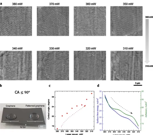
Figure 3demonstrates the morphology and surface character-istics of the obtained graphene patterns on the PVC substrate. The depth of the grooves on the MLG surface produced via laser structuring of the Ni catalyst is gradually reduced by decreasing the laser power for every 10 mW (Figure 3a). We observe disordering of the graphene surface and formation of a larger number of grain boundaries and defects. It turns out that the alignment of graphene nanostructures directly depends on the deepness of patterns in the Ni foil, and the resultant graphene pattern serves as a holding lattice.
Tailoring of graphene-surface wettability and understanding its response to different environmental conditions are the major steps toward the development of efficient graphene-based appliances in biosensorics.29
To characterize the surface capabilities of graphene patterns, we place a drop of DI on the surface of pristine and patterned MLG (Figure 3b). Obviously, the location of water drops indicates distinctive wettability of graphene zones at a contact angle ≤90°(Figure 3c). Normally, single-layer graphene is hydrophilic, which means that its WCA is≤90° (corresponds
to a high wettability) and the graphene surface is chemically active.30When we increase the number of graphene layers, the WCA is about≥90°, which corresponds to low wettability.31It implies that the surface of MLG is hydrophobic and consequently more inert. But in this study, we demonstrate an opposite resultthe surface of MLG is hydrophilic.Figure 3c shows the variation of the contact angle as a function of laser power. It is observed that the WCA increases from a value of 75° to 89.52° after the gradual laser treatment of the MLG surface, and this value remains nearly 90° (Figure S1andTable S1). Although WCA data provide valuable information on the wettability of the p-MLG surface, other surface features adhesion (Wpw) and surface free energy (γp)are the key
parameters characterizing the surface and its interaction with other materials. Besides, these parameters are closely related not only to wettability but also to many other important properties at the surface/interface and friction.32Therefore, we calculated the adhesion and surface free energy of graphene patterns based on the contact angle data by the Young−Dupre equations:33γw(1 + cosθ0) = Wpwandγp=γw/4(1 + cosθ0),2 where θ0 is the contact angle at equilibrium, γw is the water
surface energy (73 mJ/m2), Wpw is the adhesion energy of
water to the MLG surface, andγpis the surface free energy. Hence, we determined that the surface energy of p-MLG is mutually opposite to the WCA values, and by estimating the data fromTable S1, we found the highest and lowest surface energies of the p-MLG samples28.92 mJ/m2(WCA = 75°) and 18.56 mJ/m2(89.52°), respectively. Moreover, the surface energy is caused by adhesion forces which are the reason of formation of the surface bonds. Values of surface energy and
Figure 3.(a) Morphology and surface characteristics of the p-MLG. SEM images of the CVD-synthesized p-MLG on the structured Ni foil by an FS laser power treatment from 380 to 310 mW. The 5μm scaled images obtained at 30 V, 11 000−14 000× magnification. (b) Digital photograph of placing a drop of deionized water (DI) on the surface of the pristine and patterned MLG. (c) WCA (θ) on the patterned MLG surface and (d) adhesion (Wpw) and surface free energy (γp) vs laser power structuring; error is±5 units.
adhesion are always linearly proportional (Figures 3d, S2, and S3); therefore, a higher surface energy corresponds to a higher adhesion and vice versa. Our results indicate lower surface free energy of all patterned graphene samples compared to the surface free energy of water, which means that water partially wets out the graphene surface. The graphene roughness formed by laser power treatment from 380 to 310 mW determines the increase of the WCA and the surface free energy reduction, in other words, a degradation of the wettability and adhesion. The surface of the graphene produced with 310 mW laser power in comparison with the rest of the samples is more hydrophobic. To characterize the graphene patterns grown on various structured Ni foils, Raman spectroscopic analysis is performed using a laser excitation of 532 nm (Figure 4a). For single Raman measurements, 20× objective and 20 s integration time are used. The collected Raman spectra are the typical profiles of few-layer graphere/MLG. The main G- and 2D-peaks of graphene are clearly observed at around 1578 cm−1(similar for all samples) and 2695−2706 cm−1, respectively. The fixed position of G-peaks (Figure 4b) indicates stability in the planar vibrational mode of the sp2-hybridized carbon arrangement and
consequently determines the resemblance of graphene nature for all obtained patterns. The negligible 2D band shape differences and its blue shift with decreasing laser power during surface structuring are caused by the decrease of the thickness/ number of graphene layers34(Figure 4b). Analyses of the peak
intensity ratio of the 2D- and G-bands are performed (Table S2 andFigure S4). The I2D/Gratio of these bands for all graphene
patterns is equal to or less than “1”, which indicates few/ multilayeredness. The appearance of a low-intensity D-band in each case corresponds to the defect formation. Defectiveness stimulated by a laser beam via its contact with the Ni surface is manifested as afingerprint of the already imperfect structure. Nevertheless, the relatively stable I2D/G ratio in terms of laser power and sharp symmetric 2D-bands is the confirmation for a high-quality patterned few-layer graphene/MLG.
Because the groove depth of the p-MLG gradually decreases, the graphene surface roughness increases, and the surface becomes hydrophobic under laser treatment, the electrical transport property of graphene can be tuned by the surface morphology of the created patterns. Thus, the sheet resistance (Figure 4c) and optical transmittance (Figure 4d) of the p-MLG transferred on a PVC substrate are measured, and this demonstrated that patterning reduces the sheet resistance from 16 to 10Ω/sq despite the fact that the obtained p-MLG already possesses low sheet resistance (about 20 Ω/sq). Besides, we identified a directly proportional correlation between laser power and the sheet resistance of grown graphene patterns: each reduction in the laser power of pattern processing reduces the sheet resistance of the obtained p-MLG (e.g., 380 mW corresponds to 16Ω/sq and 310 mW corresponds to 10 Ω/ sq).
Figure 4.Optical and electrical properties of the p-MLG. (a) General view of Raman spectra (G-, D-, and 2D-peaks) of MLG with different patterns. (b) Variation of Raman frequency as a function of laser power. (c) Variation of the sheet resistance of p-MLG as a function of laser power. The inset shows the schematic representation of the four-point measurement system. (d) Optical transmittance of the p-MLG on the PVC substrate vs laser power.
A variation of optical transmittance of the p-MLG on the PVC substrate at around 800 nm as a function of laser power is shown inFigures 4d,S5, and S6. We observed about 1.5 times enhancement of optical transmittance with an increase of laser power from 310 to 380 mW. It is known that when the number of layers increases, the thickness becomes more uniform and results in a decrease of optical transmittance.35Apparently, the sheet thickness of the wrinkle configuration changes decreasing32 with applied lower laser power. It means that thinner and severe wrinklelike ordering of graphene with deeper structuring (380 mW obtained p-MLG) provides enhanced optical transmittance.
On the basis of the detailed morphological and electro-optical investigation of p-MLG samples, structures fabricated under 380 mW are selected. Such a graphene pattern possesses a distinct structure alignment, acting as a holding lattice which prevents defect appearance. It provides low sheet resistance (16 Ω/sq) and higher optical transmittance in comparison with other graphene patterns. Additionally, the thickest 380 mW obtained p-MLG is more hydrophilic compared to other proposed variety of patterns. The hydrophilicity provides reactivity to graphene patterns and impacts its surface area, which will significantly affect the performance of graphene-based devices. Therefore, we employed 380 mW obtained p-MLG for supercapacitor and Li-ion battery designs and compared their performance with respect to the flat graphene-based devices.
We demonstrate the optical features of a graphene-enabled supercapacitor behaving as an optical modulator. Figure 5a shows the schematic image of supercapacitor preparation. The process begins with hot lamination of MLG/p-MLG with PVC followed by etching of nickel in 1 M FeCl3·H2O solution. After
the transfer-printing process, we attached two graphene-coated PVC substrates using 250μm thick adhesive frames and affixed two copper wires to apply a voltage to the graphene electrodes
covered with silver-based conductive ink. The created super-capacitor cell was filled with 50 μL of ionic liquid electrolyte [DEME][TFSI] [98.5%, diethyl methyl(2-methoxyethyl)-ammonium bis(trifluoromethyl sulfonyl)imide], Sigma-Aldrich item#727679).
The change of the optical transmittance of a supercapacitor with patterned (Figure 5b) and flat MLG electrodes (Figure 5c) is measured by using a Bruker VERTEX 70v Fourier-transform infrared spectrometer, in which the spectral range is from 500 to 1100 nm. The optical change is performed by applying a voltage in the range of 0−5 V for both devices; the transmission condition is normalized at 0 V, which confirms the stability of supercapacitors. At 0 V, the transmittance is only 1− 2% for both devices and slightly varies with the wavelength. On applying 5 V for an MLG-enabled device, the transmittance increases sharply to 19% at 750 nm, whereas on applying 3.5 V for p-MLG-enabled device, the transmittance increases atfirst to 16% at 950 nm. At 5 V, the supercapacitor based on p-MLG demonstrates the second stage of the transmittance increase 32% at 800 nm.
The observed“2” times increase in the transmittance value of the device with p-MLG compared to that of the MLG-based device indicates the double stepwise electrostatic doping effect on graphene, which happened during intercalation of electro-lytes: at first in the thinner part (grooves) and then in the thicker part (wrinkles). As a result, the transmittance enhancement occurs because of the light beam interaction with the patterns where the p-MLG thickness is reduced grooves part. At this point, the light scattering decreases and light transmission increases accordingly. Therefore, the light throughput of the p-MLG-enabled device will be higher compared to that of the MLG-enabled device.
We also defined high modulation depths36of about 9 and 6 dB for p-MLG- and MLG-based devices, respectively. Because the variety of optical modulator applications is determined by
Figure 5.MLG-enabled supercapacitor. (a) Schematic image of supercapacitor preparation:first stagelamination with PVC at 120 °C, second stageetching of catalyst with 1 M iron chloride solution, and third stagedevice fabrication. Normalized change in the transmission of a supercapacitor with (b) patterned and (c)flat MLG electrodes using an ionic liquid as an electrolyte for bias voltage in the range of 0−5 V.
the high modulation depth (>7 dB, as high-rate interconnects and high-sensitivity sensing) and is limited when the modulation depth is less than∼4 dB (as passive mode-locking and short-distance data transmission),37it is crucial to acquire the modulation depth increase. Our results indicate broader applicability for p-MLG-enabled devices and their capability to operate in the visible range as far as we are able to increase the modulation depth index by 1.5 times.
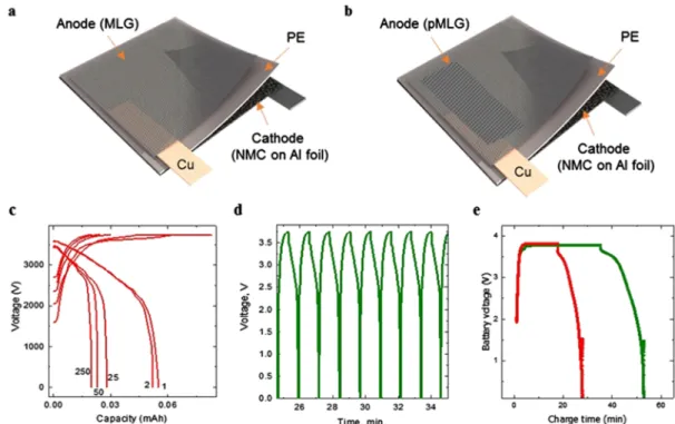
Figure 6represents a graphene-enabled battery structured as a typical Li-ion battery. This device posturizes a single-cell battery, where the electrodes are sandwiched symmetrically (Figure 6a,b). As an anode, we placed MLG/p-MLG on the polymer substrate, which acted as an electrochromic layer as well. To make good contact, we set a copper frame attached to the graphene electrode. Lithium nickel manganese cobalt oxide (known in battery manufacturing as an NMC, Litarion) is operated as a charge counter electrodecathodeproviding a reversible electrochemical reaction. Finally, the electrodes are separated using a 20μm thick porous polyethylene membrane (PE, 42% porosity, Targray) soaked with 1 M lithium hexafluorophosphate solution in ethylene carbonate and ethyl methyl carbonate (Sigma-Aldrich item#746738).
We measured the capacitance of the MLG-enabled Li-ion battery approximately 250 times, demonstrating negligible decrease of its value with each next charging/discharging cycle (Figure 6c). Inherently, all batteries gradually discharge eventually whether they are used or not. This capacity loss is typically caused by slow parasitic reactions occurring within the battery. The life cycle is the key for the good performance of a battery, and thus, increasing the life cycle is one of the first parameters that should be focused on when aiming at providing efficiency of Li-ion batteries. Usually, heteroatom doping,
chemical impregnating, and hybridization of graphene electro-des are the best approaches to improve the prolongation of Li-ion batteries. For example, a graphene hybrid-based battery can yield 400 discharge/charge cycles with 0.01% capacity loss per cycle.38 A battery in which the graphene electrode is impregnated with sulfur demonstrates ultralong viability (2000 cycles and 0.028% capacity decay per cycle).39 In our case, the proposed battery with pure MLG demonstrated operation for 1000 cycles (Figure 6d), which together with the assessed capacity (0.01% capacity loss per cycle) demonstrates promising results.
On the other hand, the internal charge/discharge efficiency plays a key role as well because slow discharging and fast charging designed in a way to reduce the impact of self-heating is required. To analyze the battery performance, the voltage dependence of charging/discharging processes by applying constant current (3 mA) for both devices is provided (Figure 6e). We observed productivity reduction in the p-MLG-based battery when compared to the MLG-based battery because of a decrease of the charge/discharge time by approximately “2” times. This allows us to predetermine the viability of the p-MLG-enabled Li-ion battery during 500 cycles. The reduction in the number of life cycles is due to the change in the graphene surface area after the patterning procedure. In fact, the patterns are artificially ordered defects that make graphene structure more loosened and promote faster intercalation/deintercalation of Li-ions. Therefore, the presented approach could lead to new bifunctional applications combining the properties of energy storage and electrically switchable devices.
Figure 6.Graphene-enabled Li-ion battery. (a) Schematic image of the symmetrically constructed secondary battery based on the flat and (b) patterned MLG. MLG/p-MLG acted as an electrochromic layer (anode). Lithium nickel manganese cobalt oxide operated as a charge counter electrode (cathode), providing a reversible electrochemical reaction in devices operating in the transmissive/reflective modes. (c) Galvanostatic discharge/charge curves of the MLG-based battery after 1st, 2nd, 25th, 50th, and 250th measurements and (d) its life cycle as a function of time. (e) Voltage profiles for the constant current charge and discharge of Li-ion batteries incorporating MLG (green curve) and p-MLG (red curve) as negative electrodes. The optical change results from an electric current of≈3 mA at low dc potentials.
ordering and, consequently, the formation of reactive oxygen-based functional groups. The distinct graphene structure alignment (which prevents defect appearance) assisted by the strongest laser power (380 mW) contributes to certain p-MLG electro-optical changes (sheet resistance decrease and optical transmittance enhancement). The p-MLG ability to operate as an electrically reconfigurable medium for supercapacitor and Li-ion battery designs are represented. The p-MLG-based supercapacitor testing results reveal 2 times transmittance value increase (in comparison with the MLG-based super-capacitor) caused by light interaction with patterned structures where its thickness is reduced. The p-MLG-based battery indicates long-life viability (500 charging/discharging cycles) with 0.01% capacity loss per cycle; the negative feedback leading toward twice the device productivity reduction which occurred due to graphene structure loosening after patterning and, consequently, (de)intercalation process accelerating. We anticipate the NLL-based p-MLG to be a new approach to overcome the limitations imposed by the existing postsynthesis processes which will open a wide applicability gateway for advanced graphene-based devices in energy storage, wearable electronics, and biosensorics.
■
METHOD SUMMARYNonlinear Laser Lithography. The nanostructuring setup consists of a FS laser system, GS, and motorized 3D-S (Figure 1). The FS system is a home-made Yb-dopedfiber laser (1030 nm) which was reported before.40 It involves a dispersion-managed oscillator, afiber stretcher, several amplification stages and a grating compressor. The stretcherfiber was distributed between the amplifier stages to provide the optimal pulse peak power during amplification to balance between the gain-narrowing and the self-phase modulation. The laser can produce up to 1μJ of pulse energy at a repetition rate of 1 MHz, which corresponds to 1 W of average power. The minimal pulse duration which can be obtained from the system is 100 fs. Because the output light of the laser is linearly polarized, the HWP placed between the laser and the polarization beam splitter provides control of the laser power on the sample. The second HWP allows the control of polarization on a sample. The sample was placed on the motorized 3D stage in the focal plane of the GS f-theta lens.
The laser beam was scanned over the nickel surface in the way that during every line scan it was partially overlapped with the already created structure. In this way we preserved the concept of nonlinear laser lithography,22which allows coherent extension of the created structure over a large area surface, thus, improving the quality of the structure. The maximum scanning area for our model of GS is 1× 1 cm2. To extend the area, XY
translation stage was used. With the given pulse energy and repetition rate, the processing speed in our work was as fast as 15 s for 1× 1 cm2area. It can be increased in the future by
heating till the temperature is raised to 1000°C. Once 1000 °C temperature was reached, the methaneflow is established at 30 sccm together with the Ar/H2flow at 100/100 sccm, followed by a waiting time of 5 min. In the end, the CH4flow is turned
off and the system is cooled down to room temperature in ∼1 h while keeping the Ar/H2flow environment at 100/100 sccm.
Transfer Printing of Multilayer Graphene. The following steps are needed for the analysis of the MLG/p-MLG surface and fabrication of graphene-enabled devices after CVD growth on a Ni foil. First, one side of the graphene-covered Ni foil was protected by paper, whereas the other side was in contact with PVC. Second, the patch of paper/ graphene/Ni/graphene/PVC was sent through a lamination machine with a temperature of about 120 °C. The obtained PVC/graphene/Ni samples were then dipped in a 1 M FeCl2
aqueous etching solution for a few hours. After the nickel was etched, the PVC/graphene membranes were placed in DI for a few hours and rinsed as well. Then, the samples were blow-dried with N2gas and were ready to use.
Characterization Methods. WCA of the MLG/p-MLG on PVC substrate was obtained using a home-made contact angle measurement setup. The setup consists of the following elements: a white LED, XYZ translation stage with standard micrometers (Thorlabs), video camera (Thorlabs, DCC1645C-USB 2.0 CMOS camera, 1280× 1024, color sensor), and usual medical syringe with a 200μm diameter needle. We put a DI water droplet of 4μL on the investigated graphene surface and took digital photographs. We measured the contact angles using a program Screen Protractor which allows us to easily and quickly measure any angle on the screen to the nearest degree. The morphological analyses of the investigated graphene samples were performed using scanning electron microscopy (Nova NanoSEM 600). To determine the graphitization fingerprint and compare the defectiveness of MLG and p-MLG surfaces, a Jobin Yvon HORIBA Raman microscope system with 20× microscope objectives and 20 s integration time was used. The excitation wavelength was 532 nm. The transmittance measurements in the wavelength range between 450 and 1100 nm were performed by using a Bruker VERTEX 70v Fourier-transform infrared spectrometer integrated with a Si photodiode. The sheet resistance measurements were carried out at four probe station platforms with the support of a Keithley 2600 multimeter. MLG was attached on the patterned area to make Ohmic contact with the four electrodes. Then, sheet resistance was calculated using the standard formula (Rs= πR/ln 2 ≈ 4.53R).
Device Performance Characterization. Graphene-En-abled Supercapacitors. Optical measurements were performed in the 450−1100 nm wavelength range by a Bruker VERTEX 70v Fourier-transform infrared spectrometer equipped with a Si photodiode. Transmittance, Tp(λ), spectra were recorded by
graphene-based supercapacitors biased using the Keithley 2400 Source measure unit.
Graphene-Enabled Li-Ion Battery. The voltage and time readings of charging/discharging processes were generated using the Keithley 2600 Source Meter instrument. The data were collected under a constant current of 3 mA and processed with LabVIEW software.
■
ASSOCIATED CONTENT*
S Supporting InformationThe Supporting Information is available free of charge on the ACS Publications websiteat DOI:10.1021/acsomega.7b01853. Surface characteristics of patterned MLG; Raman characterization; and optical characterization (Figures S5 and S6) (PDF)
■
AUTHOR INFORMATIONCorresponding Author
*E-mail:[email protected](E.K.).
ORCID
Evgeniya Kovalska:0000-0002-8996-0790 Anna Baldycheva:0000-0002-2616-595X Coskun Kocabas: 0000-0003-0831-5552
Notes
The authors declare no competingfinancial interest.
■
ACKNOWLEDGMENTSThis research was partially supported by the European Research Council (ERC) Consolidator grants ERC-682723 SmartGraphene and ERC-617521 NLL; the European Union funding: Marie Curie Fellowship visiting grant; and the Engineering and Physical Sciences Research Council (EPSRC) of the United Kingdom via grant no. EP/ N035569/1. We thank our colleagues Dr. Nurbek Kakenov, Dr. Osman Balci, and Dr. Nassima Afshar Imani from Bilkent University who provided insight and expertise that greatly assisted the research. We thank Dr. Omer Salihoglu (TUBITAK, Marmara Research Center) for the assistance with capacity and life-cycle battery measurements, and Murat Güre and Ergun Karaman (physicists and engineers of Bilkent University) for catalyst preparation and technical support. E.K. would also like to show her gratitude to all co-authors for sharing their pearls of wisdom and comments during the preparation of manuscript that greatly improved its quality.
■
REFERENCES(1) Neto, A. H. C.; et al. The electronic properties of graphene. Rev. Mod. Phys. 2009, 81, 109.
(2) Choi, W.; et al. Synthesis of graphene and its applications: A review. Crit. Rev. Solid State Mater. Sci. 2010, 35, 52.
(3) Shao, Y.; et al. Graphene based electrochemical sensors and biosensors: A review. Electroanalysis 2010, 22, 1027.
(4) Zhang, Y.; et al. Review of chemical vapor deposition of graphene and related applications. Acc. Chem. Res. 2013, 46, 2329.
(5) Han, M. Y.; et al. Energy band-gap engineering of graphene nanoribbons. Phys. Rev. Lett. 2007, 98, 206805.
(6) Hicks, J.; et al. A wide-bandgap metal−semiconductor−metal nanostructure made entirely from graphene. Nat. Phys. 2013, 9, 49.
(7) Järvinen, P.; et al. Molecular self-assembly on graphene on SiO2
and h-BN substrates. Nano Lett. 2013, 13, 3199.
(8) Kang, S. J.; et al. Inking elastomeric stamps with micro-patterned, single layer graphene to create high-performance OFETs. Adv. Mater. 2011, 23, 3531.
(9) Tapasztó, L.; et al. Tailoring the atomic structure of graphene nanoribbons by scanning tunnelling microscope lithography. Nat. Nanotechnol. 2008, 3, 397.
(10) Zhang, L.; et al. Photocatalytic patterning and modification of graphene. J. Am. Chem. Soc. 2011, 133, 2706.
(11) Jiao, L.; et al. Narrow graphene nanoribbons from carbon nanotubes. Nature 2009, 458, 877.
(12) Kosynkin, D. V.; et al. Longitudinal unzipping of carbon nanotubes to form graphene nanoribbons. Nature 2009, 458, 872.
(13) Zhang, W.; et al. Direct writing on graphene “paper” by manipulating electrons as “invisible ink”. Nanotechnology 2013, 24, 275301.
(14) Feng, J.; et al. Patterning of graphene. Nanoscale 2012, 4, 4883. (15) Pang, S.; et al. Patterned graphene electrodes from solution-processed graphite oxide films for organic field-effect transistors. Adv. Mater. 2009, 21, 3488.
(16) Kim, K. S.; et al. Large-scale pattern growth of graphene films for stretchable transparent electrodes. Nature 2009, 457, 706.
(17) Park, J. B.; et al. Fast growth of graphene patterns by laser direct writing. Appl. Phys. Lett. 2011, 98, 123109.
(18) El-Kady, M. F.; et al. Laser scribing of high-performance and flexible graphene-based electrochemical capacitors. Science 2012, 335, 1326.
(19) Strong, V.; et al. Patterning and electronic tuning of laser scribed graphene for flexible all-carbon devices. ACS Nano 2012, 6, 1395.
(20) Chang, T.-L.; et al. Patterning of multilayer graphene on glass substrate by using ultraviolet picosecond laser pulses. Microelectron. Eng. 2016, 158, 1.
(21) Kalita, G.; et al. Femtosecond laser induced micropatterning of graphene film. Mater. Lett. 2011, 65, 1569.
(22) Öktem, B.; et al. Nonlinear laser lithography for indefinitely large-area nanostructuring with femtosecond pulses. Nat. Photonics 2013, 7, 897.
(23) Sipe, J. E.; et al. Laser-induced periodic surface structure I: theory. Phys. Rev. B: Condens. Matter Mater. Phys. 1983, 27, 1141.
(24) Ardron, M.; et al. A practical technique for the generation of highly uniform LIPSS. Appl. Surf. Sci. 2014, 313, 123.
(25) Bonse, J.; et al. Femtosecond laser-induced periodic surface structures. J. Laser Appl. 2012, 24, 042006.
(26) Sun, Q.; et al. Nanograting formation on the surface of silica glass by scanning focused femtosecond laser pulses. Opt. Lett. 2008, 33, 2713.
(27) Birnbaum, M. Semiconductor surface damage produced by ruby lasers. J. Appl. Phys. 1965, 36, 3688.
(28) Martins, L. G. P.; et al. Direct transfer of graphene onto flexible substrates. Proc. Natl. Acad. Sci. U.S.A. 2013, 110, 17762.
(29) Xu, K.; et al. Wetting: Contact with what? Nat. Mater. 2013, 12, 872.
(30) Li, Z.; et al. Effect of airborne contaminants on the wettability of supported graphene and graphite. Nat. Mater. 2013, 12, 925.
(31) Raj, R.; et al. Wettability of Graphene. Nano Lett. 2013, 13, 1509.
(32) Chaudhury, M. K.; et al. Interfacial interaction between low-energy surfaces. Mater. Sci. Eng., R 1996, 16, 97.
(33) Duca, M. D.; et al. Surface modifications of polyvinylidene fluoride (PVDF) under rf Ar plasma. Polym. Degrad. Stab. 1998, 61, 65. (34) Ferrari, A. C.; et al. Raman spectrum of graphene and graphene layers. Phys. Rev. Lett. 2006, 97, 187401.
(35) Zhu, S.-E.; et al. Optical transmittance of multilayer graphene. Europhys. Lett. 2014, 108, 17007.
(36) Reed, G. T.; et al. Silicon optical modulators. Nat. Photonics 2010, 4, 518.
(37) Sun, Z.; et al. Optical modulators with 2D layered materials. Nat. Photonics 2016, 10, 227.
(38) Sun, Y.; et al. Reconstruction of conformal nanoscale MnO on graphene as a high-capacity and long-life anode material for lithium ion batteries. Adv. Funct. Mater. 2013, 23, 2436.
(39) Zhou, G.; et al. A graphene−pure-sulfur sandwich structure for ultrafast, long-life lithium−sulfur batteries. Adv. Mater. 2014, 26, 625.