PAPER
Cite this:Nanoscale, 2018, 10, 21842
Received 12th July 2018, Accepted 30th October 2018 DOI: 10.1039/c8nr05626a rsc.li/nanoscale
Onset of vertical bonds in new GaN multilayers:
beyond van der Waals solids
†
A. Onen,
aD. Kecik,
b,aE. Durgun
*
aand S. Ciraci*
bA suspended single layer of GaN in a honeycomb structure is stable in a planar geometry. By stacking these GaN layers one can construct bilayers or multilayers, even new three-dimensional (3D) periodic structures. In this study, we clarified how the planar layers are buckled with the onset of vertical Ga–N bonds. Among the four stable phases of bilayer GaN, only one of them maintains the planar geometry, which is bound by weak van der Waals interactions. For the remaining three phases, the layers are buckled with the onset of weak vertical bonds, and attain total energies slightly lower than that of the planar geo-metry. Structural phase changes, as well as direct–indirect band transitions take place under strain and electrostatic charging. The vertical bonds become shorter in multilayers, and eventually attain the bulk value. Among the stable phases of 3D periodic GaN, only one with a graphite-like structure behaves as a layered, van der Waals solid; whereby others are 3D uniform crystals beyond the van der Waals solid.
Introduction
Gallium nitride (GaN) crystal in wurtzite structure (wz-GaN) is an important wide band-gap semiconductor with a critical and wide range of technological applications in microwave com-munications, lasers, detectors, and light-emitting diodes in the ultraviolet range.1–3As early as 2005, first-principles calcu-lations predicted that the GaN compound can form the free-standing, graphene-like, single-layer (SL) h-GaN structure.4 Later, extensive analyses of dynamical5and thermal stability6 have demonstrated that free-standing, SL h-GaN is, in fact, stable in the planar honeycomb structure. Planarity, which is common to SL compounds like h-BN, h-GaN, and h-AlN that involve at least one element from the first row of the Periodic Table, is maintained by π-bonds between p-orbitals of the nearest cation and anion atoms. Conversely, silicene, germa-nene, and h-GaAs are buckled.5,7,8Recently, numerous theore-tical studies unveiled diverse aspects of h-GaN;9in particular they predicted that stable bilayer, multilayer and layered allo-tropes of h-GaN can form with tunable optoelectronic properties.6,9–12Much recently, the synthesis of ultrathin two-dimensional (2D) h-GaN on SiC via graphene encapsulation
method by Al Balushi et al.13has brought 2D GaN further into focus.
While multilayers of 2D GaN, AlN, SiC, silicene, and germa-nene can be constructed, the important question of whether these materials are similar to van der Waals (vdW) solids with weak interlayer coupling leading to wide interlayer spacings, or if vertical chemical bonds may occur, gained significant importance. In fact, layered silicite7,8,14,15and germanite struc-tures with vertical covalent bonds were proposed to explain the data taken from multilayers of silicene and germanene. So far the structures of multilayer silicene and germanene have not been fully resolved. Similarly, SL h-GaAs is buckled;4,5vertical bonds form readily in its multilayers. Incidentally, it was argued that the graphitic structure of few-layer planar h-GaN is unstable and reconstructs into a structure with specific vertical bonds, whereby alternating square and octagon rings appear, nevertheless the in-plane buckled honeycomb structure is maintained.16 Haeckelite structures in single and multilayer square-octagon GaN have been predicted to be stable.17–21The analysis of electronic charges revealed formation of weak, covalent + ionic vertical bonds.21
Onset of the vertical bonds with a mixed covalent + ionic nature between specific cation and anion pairs in adjacent planes with AA′A.. conformation, while expanding the distance between other pairs, is a complex interplay between sp2–sp3 hybridization dictated by the energy minimization. Their mul-tilayers constructed by stacking of planar, SL graphene, h-BN and h-AlN remain planar with wide interlayer distances coupled with weak vdW interactions, forming typical vdW solids. Therefore, it is of current interest to know whether mul-tilayers of planar, SL h-GaN can construct layered structures
†Electronic supplementary information (ESI) available. See DOI: 10.1039/ C8NR05626A
aUNAM - National Nanotechnology Research Center and Institute of Materials
Science and Nanotechnology, Bilkent University, Ankara, 06800, Turkey. E-mail: [email protected]
bDepartment of Physics, Bilkent University, 06800 Ankara, Turkey.
E-mail: [email protected]
Published on 01 November 2018. Downloaded by Bilkent University on 2/25/2019 9:39:58 AM.
View Article Online
with weak interlayer coupling like vdW solids. Answering this question is very critical in the sense of paving the way towards new artificial three-dimensional (3D) layered crystals, or thin films exhibiting novel physical properties different from the parent 3D homogeneous crystals.
In this study, we examined the onset of vertical bonds in bilayer (B), trilayer (T), and periodic multilayers of h-GaN, and their effects on the electronic structure within first-principles density functional theory (DFT) calculations. Firstly, the nature of these vertical bonds in diverse multilayers of GaN is ana-lyzed. We found that both planar bilayer (B-PL) and buckled, haeckelite-type bilayer (B-HK) phases possess dynamical and thermal stability, with a minute gain of energy by the onset of vertical bonds upon transforming from B-PL to B-HK, within the accuracy limits of DFT. However, the energy difference between them increases with increasing number of layers. The structural transition from B-PL to B-HK cannot occur spon-taneously; it requires an external excitation to overcome the energy barrier between the two phases. Surprisingly, in con-trast to what has been assumed so far,16the haeckelite struc-ture is not the lowest energy strucstruc-ture; instead there are mani-folds of bilayer structures, which are energetically favorable. These phases of GaN bilayers display interesting structural changes and also direct–indirect band gap transitions by the applied strain and electrostatic charging. We also found that layered, as well as new 3D bulk structure can be constructed despite the fact that 3D wurtzite structure is a global minimum. Another striking, insofar surprising result is that all manifolds of bilayer and 3D periodic structures mark similar fundamental band gaps despite their significant struc-tural differences set by the vertical bonds.
Method
The theoretical predictions of the ground state properties of 2D and periodic/bulk forms of GaN discussed in this paper are based on first-principles calculations performed using DFT. In the majority of the calculations presented, the plane-wave basis set together with the projector-augmented-wave poten-tials (PAW) formalism22,23implemented in the Vienna ab initio simulation package (VASP)24,25is used. The electron exchange and correlation potential is described by the Perdew–Burke– Ernzerhof (PBE) form within the generalized gradient approxi-mation (GGA), with d-electrons also taken into account (GGA-d XC potential).26,27 Van der Waals interactions are accounted for the layered, periodic and bulk structures using the Grimme method.28,29 Atomic positions are optimized using the conjugate gradient (CG) method; the total energy and atomic forces are minimized with specific criteria for energy difference convergence. Monkhorst–Pack30 k-point sampling adopted for the PBE calculations of the 2D unit cell is 25 × 25 × 1, and 19 × 19 × 19 for the periodic and bulk structures.
Various energy criteria for quantifying the interactions can be summarized as: the cohesive energies of layered allotropes of GaN relative to their constituent free atoms are calculated
from the expression, Ec= ET[Ga] + ET[N]− ET[GaN] in terms of
the total energies ET[Ga] and ET[N] of free Ga and N atoms,
respectively, and the optimized total energy, ET[GaN] per Ga–N
pair of a specific allotrope. The higher the positive Ec, the
stronger is the binding. By subtracting the cohesive energy of the structure in the global minimum (namely cohesive energy of 3D wurtzite structure) from that calculated for other 3D and 2D allotropes, one obtains the formation energy Efat T = 0 K
relative to the global minimum. A specific allotrope can corres-pond to a local minimum on the Born–Oppenheimer surface and hence can remain stable in spite of the fact that it has a negative Ef. The average binding energy of layers in a multilayer
structure can be expressed as Ei = ET[SL GaN]− ET[ML GaN]
relative to constituent SL GaN. Cohesive, formation and binding energies are given per Ga–N pair. The characters of bonds are analyzed by the contour plots of the total charge density,ρT, the difference charge density (i.e. Δρ = ρT− ρGa,N).
The interionic charge transfer between Ga and N in different allotropes and the bond orders (BO) are calculated based on the DDEC6 method.31,32
The dynamical stability of the 2D and periodic allotropes is tested by ab initio phonon calculations.33A structure having positive vibrational frequencies, Ω(k) > 0, for all k in the Brillouin zone, assures dynamical stability at T = 0 K. Finite displacement method is employed using the Phonopy code,34 with 4 × 4 × 1 and 2 × 2 × 2 rectangular cell samplings for the bilayer and 3D periodic structures, respectively. The stability of the phases under thermal excitations is crucial, since an allo-trope that is dynamically stable at T = 0 K can experience instability even at low temperatures. The stability of the 2D allotropes of GaN against thermal excitations is tested by per-forming finite-temperature ab initio molecular dynamics (MD) calculations. Accordingly, in the microcanonical ensemble, the velocities are scaled at each time step (of 2 fs) in order to keep the temperature constant, where we begin with 150 K, and increase to 300 and 450 K, each simulation time for each temp-erature lasting 2 ps, and 6 ps in total. In specific cases, the temperature is raised up to 1000 K. Moreover, MD simulations are repeated by using the canonical ensemble with Nosé ther-mostat,35carried out at 150 K, 300 K, and 450 K.
In addition to the standard-DFT results, the calculations undertaking hybrid functionals (HSE, where a quarter of the exact exchange is incorporated in the XC functional)36–38 are also included, in order to obtain the corrected band structures of 3D bulk and 2D layered GaN structures.
Results and discussion
Single-layer, free-standing, h-GaN is planar and constitutes the basic element of various structures treated in this study. For the sake of comparison, we reproduced its structural para-meters, cohesive and formation energies at T = 0 K, as well as the fundamental band gaps. Its 2D rectangular lattice para-meters are a = 6.42 and b = 5.57 Å, the cohesive energy is Ec=
8.29 eV, and the formation energy is Ef = −1.16 eV, with an
indirect fundamental band gap of Eg = 2.16 eV calculated by
PBE,26,27which is raised to 3.42 eV after the HSE correction.36–38 Among various stacking sequences, two SL’s of h-GaN with a uniform interlayer spacing of∼2.47 Å in AA′ conformation, which is specified as planar bilayer (B-PL), have a cohesive energy of Ec= 8.57 eV (Fig. 1). This interlayer spacing, which is
larger than the usual Ga–N bond distance (1.88 Å), does not allow the vertical bond formation, hence the layers are bound by weak vdW attraction. The binding energy of two layers rela-tive to the free SL h-GaN is 280 meV per Ga–N pair; which is not high. In order to eliminate any constraints due to the small cell size, the structural optimizations were performed in a cell including 8 Ga and 8 N atoms. Furthermore, dynamical and thermal stability tests including vdW interactions indicate that B-PL is indeed a stable structure, despite its negative for-mation energy of Ef=−0.87 eV. Incidentally, at T = 450 K the
planarity ceases; random and transient vertical bonds start to form between the two layers. The structure appears to be in a
local minimum in the Born–Oppenheimer energy surface, since it did not transform spontaneously into a different one like the haeckelite structure, which was found to have lower energy.16This relaxation was repeated in a (4 × 4) super cell to avoid any restrictions that may arise from the unit cell size, whereby no spontaneous transition took place.
In order to clarify this paradoxical situation, this time we started from the buckled h-GaN displaying a haeckelite-like structure (B-HK) from the side view, consisting of octagons and squares. The optimized structure has strong lateral bonds of dl= 1.85–1.88 Å. However, weak vertical bonds of dv= 2.30 Å
formed between specific Ga and N atoms in adjacent layers, while the distance between other Ga and N atoms increased to 2.87 Å (Fig. 1). Eventually, the B-HK structure was revealed as only 5 meV energetically more favorable relative to B-PL. This structure is found to be stable also based on the dynamical stability analysis at T = 0 K and thermal stability analysis at T = 450 K (Fig. S1, ESI†).
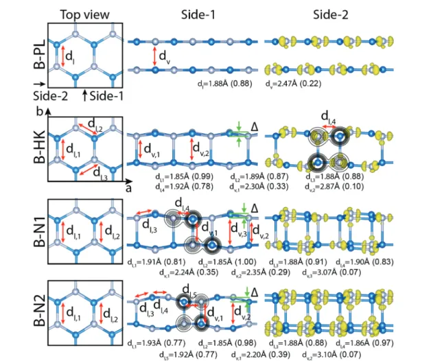
Fig. 1 Characterization of the allotropes of the GaN bilayer: planar, B-PL; haeckelite-like, B-HK; new allotropes, B-N1; B-N2. Atomic configurations: Left panels: Top view in the rectangular unit cell comprising 8 Ga–N pairs. Ga and N atoms are shown by gray and blue atoms. a and b are lattice constants. Middle panels: Side view-1 along y-direction. Contour plots of ρTshow that higher charge density is shifted towards the N atom. Right
panels: Side view-2 along x-direction. Isosurfaces of the difference charge density, Δρ indicates strong and weak bond charges of the lateral and ver-tical bonds, respectively. Ionic character of the bond becomes apparent with the bond charges shifting towards the anion. Optimized values of the lateral, dland vertical, dvbonds and their calculated bond orders (in parenthesis) are given for each bilayer structure. Isosurface values are set to
0.22e bohr−3.
Our search for the allotropes of bilayers resulted in two new, stable, bilayer configurations, specified as B-N1 and B-N2 as shown in Fig. 1; both of them having cohesive energies even higher than that of B-HK. In particular, the B-N2 structure is 17 meV (or 136 meV per cell) energetically more favorable than B-HK. In Fig. 1, we present the atomic configurations, struc-tural parameters, and charges of the lateral and vertical bonds of all four structures of GaN bilayers. The perspective views of the four bilayer structures are shown in Fig. S2, ESI.† While all phases have similar top views of a hexagonal structure, side views differ significantly. The vertical bonds, which start to form between specific Ga and N atoms in different layers, are of crucial importance and are examined in terms of the isosur-faces of the difference charge, contour plots and bond orders (BO)31,32(the latter as a measure for the strength of a bond) in Fig. 1. In bilayers, the vertical bonds are longer than the usual in-plane lateral Ga–N bonds. Accordingly, the bond orders rele-vant to the lateral, in-plane Ga–N bonds are as high as 0.88. The distance between Ga and N atoms in different planes of B-PL is 2.47 Å and the corresponding BO is 0.22.
In B-HK, the vertical bonds with dv= 2.30 Å and BO = 0.33
are still longer and hence weaker than the lateral Ga–N bonds, nonetheless shorter than the interlayer distance of B-PL. The most energetic bilayer, B-N2 has the shortest vertical bond, dv=
2.20 Å, at the same time the highest bond order, BO = 0.39 among four bilayer structures. Additionally, molecular dynamics (MD) simulations of the B-N2 structure sustained at 1000 K, except that the positions of the vertical bonds change randomly in the course of the simulation. In the light of this discussion, one can argue that the vertical bonds set in bilayers are longer, and differ from the usual, strong Ga–N bonds. Generally, their length and strength determine the stability or energetics of the structure. Nevertheless, as the number of layers increases in multilayers, the vertical bonds are further shortened and even-tually attain the strength of the bulk bonds. Incidentally, the cohesive energy of trilayer T-HK becomes higher than that of T-PL, as well as T-N2. In Table 1 the optimized values of struc-ture parameters, bond orders, energetics and energy band gaps of bilayer and 3D periodic structures are presented.
Four bilayer structures undergo interesting structural tran-sitions under biaxial strain/stress. This suggests that these structures are in local minima separated by small energy
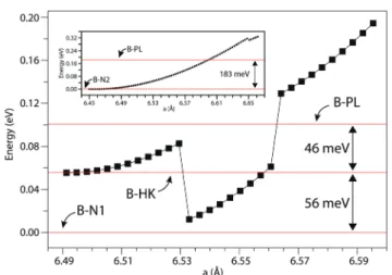
bar-riers. Fig. 2 summarizes the structural phase changes among the bilayer phases under biaxial strain. If one starts with the haeckelite-like structure B-HK, the variation of energy initially follows a parabolic curve, however drops suddenly at a = 6.53 Å by∼80 meV. At this point, the structure transforms to B-N1. As the strain continues to increase, the energy increases by follow-ing a steeper parabolic curve. When a > 6.56 Å, the energy raises suddenly by ∼70 meV and the structure transforms to B-PL. Thereafter, the energy continues to increase. However, if one starts from the B-N2 structure with a = 6.46 Å, the energy increases without any phase transitions until a = 6.65 Å, where the phase changes to the planar B-PL following a small drop in energy as shown by the inset in Fig. 2.
Similar structural transformations or phase changes occur under electrostatic charging. In order to show phase changes mediated by electrostatic charging, we examined only a few specific cases within plausible charging limits.39For example, B-PL displays interesting phase changes. When charged by q = −0.5e per unit cell (0.03e per atom) or q = −1.0e per unit cell (0.06e per atom), it changes to the B-N2 structure; nonetheless preserves its planar geometry when charged by q = 1.0e per
Table 1 Optimized values for monolayer (M), bilayer (B) and 3D periodic (P) structures of GaN: lattice parameters, a, b and c in Å; cohesive energy Ecin eV per Ga–N pair; total interlayer interactions, Eiin eV per Ga–N pair; formation energy Efin eV per Ga–N pair; direct (d) or indirect (i)
funda-mental band gaps calculated by PBE and corrected by HSE, Eg,d/iin eV
Allotrope a (Å) b (Å) c (Å) Δ (Å) Ec(eV) Ei(eV) Ef(eV) Eg,PBE− i,d (eV) Eg,HSE− i,d (eV)
M-PL 6.42 5.57 — — 8.286 0.000 −1.163 2.16(i) 3.42(i) B-PL 6.53 5.65 — — 8.572 0.286 −0.877 1.97(i) 3.25(i) B-HK 6.49 5.60 — 0.28 8.578 0.292 −0.872 1.83(d) 3.11(d) B-N1 6.51 5.63 — 0.06, 0.41 8.585 0.299 −0.865 1.95(i) 3.21(i) B-N2 6.46 5.61 — 0.45 8.595 0.309 −0.854 1.96(d) 3.22(d) P-PL 6.62 5.74 4.88 — 8.941 0.655 −0.508 1.23(d) 2.44(d) P-HK 6.43 5.50 5.50 0.75 9.325 1.039 −0.125 1.82(d) 3.00(d) P-N2 6.42 5.63 5.76 0.86 9.063 0.777 −0.387 1.79(d) 3.02(d) WZ 6.41 5.55 5.24 0.85 9.450 1.163 0.000 1.76(d) 3.03(d)
Fig. 2 Variation of the strain energy with lattice constants, leading to structural transformations of the bilayer structures. The lattice constants are obtained by applying uniform and tensile biaxial strain. Total energy ( per cell) of the B-N1 structure is set to 0 eV. The transformation from B-N2 to B-PL is shown as an inset.
unit cell and transforms to an intermediate state when charged by q = 0.5e per unit cell. On the other hand, if one starts from the former negatively charged B-N2 phase, the structure remains in B-N2 when charged by q = 1.0e per unit cell, and converts to an intermediate phase if it is charged by q = 2.0e per unit cell (0.13e per atom). B-HK does not transform into another phase when charged by q = ±1.0e per unit cell, however
converts to an intermediate phase for q = 2.0e per unit cell similar to the B-N2 case. B-HK, B-N1, and B-N2 preserve their geometries when charged by q = ±0.5e per unit cell. These pre-liminary tests suggest that the bilayer structures can be utilized as phase change materials and deserve further detailed analyses. In Fig. 3, we present the energy bands of four bilayers calcu-lated within PBE and corrected by HSE together with the
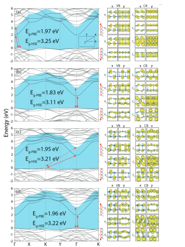
iso-Fig. 3 Left: Energy band structures of four structures of bilayers: (a) B-PL, (b) B-HK, (c) B-N1 and (d) B-N2. The fundamental band gaps determined by the HSE correction over the PBE bands are shaded. Direct or indirect band gaps calculated by PBE and HSE are marked by arrows. Right: Isosurfaces of charge density of conduction, C1, C2,… and valence band, V1, V2… states at the regarding extreme points in the Brillouin zone.
surfaces of charge density of states at the band edges (the detailed charge density analysis and partial density of states are shown in Fig. S3 and S4, ESI†). The four bilayer structures with honeycomb geometry in the top view share the rectangu-lar Brillouin zone. It is surprising that, despite the differences in the bilayer structures, the electronic energy bands look similar. Fundamental band gaps of these four bilayer struc-tures range between 3.11 eV and 3.25 eV. Apparently, the HSE band gap of SL h-GaN being 3.42 eV is reduced in bilayers due to the quantum size effect. The overall dispersions of the bands at the edge of the conduction band, in particular, near the center of the Brillouin zone appear to be similar. The bands at the edge of the valence band are generally flat, yet the slight maxima occur at different k-points. For example, in B-PL and B-N2 structures, the fundamental band gap is indirect due to a weak Mexican hat type dispersion around theΓ-point. Whereas, B-HK and B-N1 structures are direct band gap semiconductors. This direct–indirect band gap transition is an important feature among bilayer structures. The similarity of band dispersions at the band edges is revealed from the isosurfaces of charge density of the band states in Fig. 3. The bands at the edge of the valence band are constructed from pz-orbitals perpendicular
to the bilayers having only weak lateral coupling; where coup-ling in the perpendicular direction is absent. This situation is seen as the main reason for their flat dispersion. On the other hand, the high dispersion of the conduction band edge is attributed to strong lateral coupling of the directional orbitals.
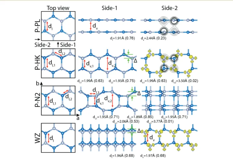
3D GaN in wurtzite structure is the allotrope of GaN in the global minimum among all allotropes in diverse dimensional-ity; each atom is fourfold coordinated where Ga–N pairs form tetrahedrally coordinated mixed bonds.40Another 3D allotrope is the zincblende structure, which has slightly higher energy.9 Here, with the premiss of revealing artificial structures with new functionalities, we explore the possibility of constructing 3D layered or quasi-layered structures as an alternative to the existing 3D crystals. Even if these layered structures were ener-getically less favorable, they can be stable in local minima and are expected to display properties different from those of 3D WZ. We considered 3D periodic new allotropes consisting of periodic planar (P-PL), periodic haeckelite (P-HK), and periodic N2 (P-N2). In Fig. 4 we show the optimized atomic configur-ations and bonding of these structures in the rectangular cell ( perspective views of these structures are given as Fig. S5, ESI†). P-PL is a real layered structure with wide interlayer spacing. It is
Fig. 4 Atomic structures and bond characterization of 3D (layered) periodic planar P-PL, haeckelite P-HK, P-N2, and wurtzite WZ structures. Left panels: Top view in the rectangular unit cell comprising 8 Ga–N pairs. a and b are lattice constants. Middle panels: Side view-1. Right panels: Side view-2. Isosurfaces of the difference charge density, Δρ are also shown. Optimized values of lateral (dl) and vertical (dv) bonds and their calculated
bond orders BO (in parentheses) are given for each structure. Isosurface values are set to 0.02e bohr−3.
a vdW solid constructed from planar h-GaN layers in AA′A′A.. conformity and preserves three fold coordination with sp2-type hybridization. It is dynamically stable in T = 0 K (Fig. S6, ESI†). However, it transforms to 3D WZ structure at T = 150 K. The P-HK structure is also dynamically stable at T = 0 K and remains stable even at T = 450 K. In the side view, it displays a periodic arrangement consisting of octagons and squares. Its vertical bonds are contracted and attain the length close to that of the lateral bond, namely dv1 = 1.99 Å with a high bond order of
BO = 0.63. All atoms are fourfold coordinated. Accordingly, it is considered a uniform crystal, except the holes or interstitial site of octagons. The cohesive energy of P-HK is 9.32 eV, which is 125 meV energetically less favorable than WZ. P-N2 is 387 meV energetically less favorable than WZ; it has vertical bonds of dv= 2.06 Å and BO = 0.53. This structure is also dynamically
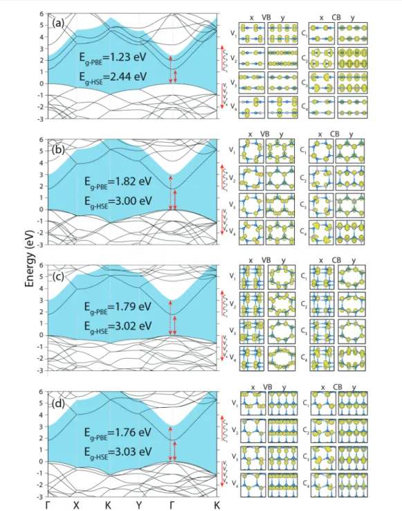
stable, and remains stable even at T = 450 K (Fig. S6, ESI†). The energy band structures of the four 3D allotropes of GaN are presented in Fig. 5 (the detailed charge density
ana-Fig. 5 Left: Energy band structures of four 3D structures of GaN. (a) Layered P-PL, (b) periodic haeckelite, P-HK, (c) P-N2 (new structure-2), (d) 3D WZ structure. Bands are calculated by PBE, and corrected by HSE. The fundamental band gaps determined by the HSE correction over the PBE bands are shaded. Direct or indirect band gaps are marked by arrows. Right: Isosurfaces of the charge density distributions of conduction, C1, C2,
and valence band, V1, V2… states at the regarding extreme points in the Brillouin zone.
lysis and partial density of states are shown in Fig. S7 and S8, ESI†). Bands are calculated by PBE, subsequently corrected by HSE. All band structures look similar in the rectangular Brillouin zone. All 3D phases have direct fundamental band gaps. The band gap of the P-PL structure is 2.44 eV. The funda-mental band gaps of the P-HK, P-N2 and P-WZ structures are, respectively, 3.00 eV, 3.02 eV and 3.03 eV; they are almost iden-tical. The details of the band edge states are presented by their charge density isosurfaces in right panels of Fig. 5. The bands at the top of the valence band gained dispersion due to the periodicity perpendicular to the layers, nevertheless their dis-persions are still lower than the disdis-persions of the bands at the bottom of the conduction band.
In summary, the previous discussion clarified an important question of whether stable layered vdW solids like graphite can be constructed by stacking of the planar, monolayer GaN, or if it will transform into different crystals by the formation of vertical bonds between Ga and N ions in adjacent layers, like silicite. By analyzing the character of the lateral and vertical bonds, we found that GaN is in between: among four different stable phases corresponding to the local minima in bilayer geometry (two of them newly predicted in this study), the energy difference between the planar bilayer bound by vdW attraction and the other three stable bilayers with weak vertical bonds is minute. Nevertheless, planar layers are buckled, even if the vertical bonds are longer and weaker than the usual GaN bonds. Among these four phases of bilayer GaN, the tran-sitions are not spontaneous, but require external excitation like strain or electrostatic charging. Transitions between two specific phases bring about also the direct–indirect transition of the fundamental band gap.
With increasing layer numbers, vertical bonds become shorter and stronger; eventually approaching the lateral GaN bonds in 3D crystals. In 3D, we found one layered vdW solid, predicted one new crystal having vertical bonds in addition to 3D wurtzite, zincblende and haeckelite structures. 3D layered ( planar) GaN is dynamically stable, nevertheless transformed to wurtzite structure at T = 150 K. Both the new crystal (P-N2) and the crystal in the haeckelite structure (P-HK) are dynami-cally stable and sustained thermal excitations at 450 K. Both have wide direct band gaps of∼3.0 eV, whereas are energeti-cally less favorable than the wurtzite structure. Accordingly, h-GaN appears to be different from vdW solids like h-BN and homogeneous crystal of silicite; since in its multilayer forms, it can lead to both vdW solid and homogeneous crystals.
Con
flicts of interest
There are no conflicts to declare.Acknowledgements
The calculations were performed at TUBITAK ULAKBIM, High Performance and Grid Computing Center (TR-Grid
e-Infrastructure) and the National Center for High Performance Computing of Turkey (UHeM) under grant no. 5003622015. This work was supported by the Scientific and Technological Research Council of Turkey (TUBITAK) under Project No. 117F241. E. D. acknowledges support from the Turkish Academy of Sciences - Outstanding Young Scientists Award Program (TUBA-GEBIP). S. C. acknowledges financial support from the Academy of Sciences of Turkey (TUBA).
References
1 S. Nakamura, M. Senoh, S.-i. Nagahama, N. Iwasa, T. Matsushita and T. Mukai, InGaN-based laser diodes with an emission wavelength of 450 nm, Appl. Phys. Lett., 2000, 76, 22–24.
2 S. Nakamura, Nobel Lecture: Background story of the invention of efficient blue InGaN, Rev. Mod. Phys., 2015, 87, 1139.
3 H. Morkoç, Handbook of nitride semiconductors and devices, Materials Properties, Physics and Growth, John Wiley & Sons, 2009, vol. 1.
4 E. Durgun, S. Tongay and S. Ciraci, Silicon and III-V com-pound nanotubes: Structural and electronic properties, Phys. Rev. B: Condens. Matter Mater. Phys., 2005,72, 075420. 5 H. Şahin, S. Cahangirov, M. Topsakal, E. Bekaroglu, E. Akturk, R. T. Senger and S. Ciraci, Monolayer honeycomb structures of group-IV elements and III-V binary com-pounds: First-principles calculations, Phys. Rev. B: Condens. Matter Mater. Phys., 2009,80, 155453.
6 A. Onen, D. Kecik, E. Durgun and S. Ciraci, GaN: From three- to two-dimensional single-layer crystal and its multi-layer van der Waals solids, Phys. Rev. B, 2016,93, 085431. 7 S. Cahangirov, M. Topsakal, E. Aktürk, H. Şahin and
S. Ciraci, Two- and one-dimensional honeycomb structures of silicon and germanium, Phys. Rev. Lett., 2009, 102, 236804.
8 S. Cahangirov, M. Topsakal and S. Ciraci, Armchair nano-ribbons of silicon and germanium honeycomb structures, Phys. Rev. B: Condens. Matter Mater. Phys., 2010,81, 195120. 9 D. Kecik, A. Onen, M. Konuk, E. Gürbüz, F. Ersan, S. Cahangirov, E. Aktürk, E. Durgun and S. Ciraci, Fundamentals, progress, and future directions of nitride-based semiconductors and their composites in two-dimen-sional limit: A first-principles perspective to recent syn-thesis, Appl. Phys. Rev., 2018,5, 011105.
10 D. Xu, H. He, R. Pandey and S. P. Karna, Stacking and elec-tric field effects in atomically thin layers of GaN, J. Phys.: Condens. Matter, 2013,25, 345302.
11 A. K. Singh and R. G. Hennig, Computational synthesis of single-layer GaN on refractory materials, Appl. Phys. Lett., 2014,105, 051604.
12 N. Sanders, D. Bayerl, G. Shi, K. A. Mengle and E. Kioupakis, Electronic and Optical Properties of Two-Dimensional GaN from First-Principles, Nano Lett., 2017, 17, 7345–7349.
13 Z. Y. Al Balushi, K. Wang, R. K. Ghosh, R. A. Vilá, S. M. Eichfeld, J. D. Caldwell, X. Qin, Y.-C. Lin, P. A. DeSario, G. Stone, et al., Two-dimensional gallium nitride realized via graphene encapsulation, Nat. Mater., 2016,15, 1166.
14 S. Cahangirov, V. O. Özçelik, A. Rubio and S. Ciraci, Silicite: The layered allotrope of silicon, Phys. Rev. B: Condens. Matter Mater. Phys., 2014,90, 085426.
15 S. Cahangirov, V. O. Özçelik, L. Xian, J. Avila, S. Cho, M. C. Asensio, S. Ciraci and A. Rubio, Atomic structure of the 3× 3 phase of silicene on Ag (111), Phys. Rev. B: Condens. Matter Mater. Phys., 2014,90, 035448.
16 A. Kolobov, P. Fons, J. Tominaga, B. Hyot and B. Andre, Instability and spontaneous reconstruction of few-mono-layer thick GaN graphitic structures, Nano Lett., 2016,16, 4849–4856.
17 D. C. Camacho-Mojica and F. López-Urías, GaN haeckelite single-layered nanostructures: monolayer and nanotubes, Sci. Rep., 2015,5, 17902.
18 H. Zhang, F.-S. Meng and Y.-B. Wu, Two single-layer porous gallium nitride nanosheets: A first-principles study, Solid State Commun., 2017,250, 18–22.
19 P. A. Brown and K. L. Shuford, Archimedean (4, 8)-tessella-tion of haeckelite ultrathin nanosheets composed of boron and aluminum-group V binary materials, Nanoscale, 2016, 8, 19287–19301.
20 A. Kolobov, P. Fons, Y. Saito, J. Tominaga, B. Hyot and B. André, Strain engineering of atomic and electronic struc-tures of few-monolayer-thick GaN, Phys. Rev. Mater., 2017, 1, 024003.
21 E. Gürbüz, S. Cahangirov, E. Durgun and S. Ciraci, Single layers and multilayers of GaN and AlN in square-octagon structure: Stability, electronic properties, and functionali-zation, Phys. Rev. B, 2017,96, 205427.
22 P. E. Blöchl, Projector augmented-wave method, Phys. Rev. B: Condens. Matter, 1994,50, 17953–17979.
23 G. Kresse and D. Joubert, From ultrasoft pseudopotentials to the projector augmented-wave method, Phys. Rev. B: Condens. Matter, 1999,59, 1758–1775.
24 G. Kresse and J. Hafner, Ab initio molecular-dynamics simulation of the liquid-metal–amorphous-semiconductor transition in germanium, Phys. Rev. B: Condens. Matter, 1994,49, 14251.
25 G. Kresse and J. Furthmüller, Efficient iterative schemes for ab initio total-energy calculations using a plane-wave basis set, Phys. Rev. B: Condens. Matter, 1996,54, 11169–11186.
26 J. P. Perdew, K. Burke and M. Ernzerhof, Generalized gradi-ent approximation made simple, Phys. Rev. Lett., 1996,77, 3865.
27 K. Burke, J. Perdew and M. Ernzerhof, Generalized Gradient Approximation Made Simple [Phys. Rev. Lett. 77, 3865 (1996)], Phys. Rev. Lett., 1997,78, 1396.
28 S. Grimme, Semiempirical GGA-type density functional constructed with a long-range dispersion correction, J. Comput. Chem., 2006,27, 1787–1799.
29 T. Bucko, J. Hafner, S. Lebegue and J. G. Angyán, Improved description of the structure of molecular and layered crys-tals: ab initio DFT calculations with van der Waals correc-tions, J. Phys. Chem. A, 2010,114, 11814–11824.
30 H. J. Monkhorst and J. D. Pack, Special points for Brillouin-zone integrations, Phys. Rev. B: Solid State, 1976, 13, 5188.
31 N. G. Limas and T. A. Manz, Introducing DDEC6 atomic population analysis: part 2. Computed results for a wide range of periodic and nonperiodic materials, RSC Adv., 2016,6, 45727–45747.
32 T. A. Manz, Introducing DDEC6 atomic population ana-lysis: part 3. Comprehensive method to compute bond orders, RSC Adv., 2017,7, 45552–45581.
33 S. Baroni, S. De Gironcoli, A. Dal Corso and P. Giannozzi, Phonons and related crystal properties from density-func-tional perturbation theory, Rev. Mod. Phys., 2001,73, 515. 34 A. Togo and I. Tanaka, First principles phonon calculations
in materials science, Scr. Mater., 2015,108, 1–5.
35 S. Nosé, A unified formulation of the constant temperature molecular dynamics methods, J. Chem. Phys., 1984, 81, 511–519.
36 J. Heyd and G. E. Scuseria, Efficient hybrid density func-tional calculations in solids: Assessment of the Heyd– Scuseria–Ernzerhof screened Coulomb hybrid functional, J. Chem. Phys., 2004,121, 1187–1192.
37 J. Heyd and G. E. Scuseria, Assessment and validation of a screened Coulomb hybrid density functional, J. Chem. Phys., 2004,120, 7274–7280.
38 J. Paier, M. Marsman, K. Hummer, G. Kresse, I. C. Gerber and J. G. Ángyán, Screened hybrid density functionals applied to solids, J. Chem. Phys., 2006,124, 154709. 39 A. Pachoud, M. Jaiswal, P. K. Ang, K. P. Loh and
B. Ozyilmaz, Graphene transport at high carrier densities using a polymer electrolyte gate, EPL, 2010,92, 27001. 40 W. A. Harrison and S. Ciraci, Bond-orbital model. II, Phys.
Rev. B: Solid State, 1974,10, 1516.