• Sonuç bulunamadı

Förster-type nonradiative energy transfer for assemblies of arrayed nanostructures: confinement dimension vs stacking dimension

N/A
N/A
Protected

Academic year: 2021

Share "Förster-type nonradiative energy transfer for assemblies of arrayed nanostructures: confinement dimension vs stacking dimension"

Copied!
8
0
0

Yükleniyor.... (view fulltext now)

Tam metin

(1)

Fo

̈rster-Type Nonradiative Energy Transfer for Assemblies of Arrayed

Nanostructures: Con

finement Dimension vs Stacking Dimension

Pedro Ludwig Hernández-Martínez,

†,‡

Alexander O. Govorov,

§

and Hilmi Volkan Demir*

,†,‡

LUMINOUS! Center of Excellence for Semiconductor Lighting and Display, School of Electrical and Electronics Engineering, Division of Physics and Applied Physics, School of Physical and Mathematical Sciences, Nanyang Technological University, Singapore 639798, Singapore

Department of Physics, Department of Electrical and Electronics Engineering, UNAMNational Nanotechnology Research Center and Institute of Materials Science and Nanotechnology, Bilkent University, Ankara 06800, Turkey

§Department of Physics and Astronomy, Ohio University, Athens, Ohio 45701, United States

*

S Supporting Information

ABSTRACT: Förster-type nonradiative energy transfer (NRET) provides us with the ability to transfer excitation energy between proximal nanostructures with high efficiency under certain conditions. Nevertheless, the well-known Förster theory was developed for the case of a single donor (e.g., a molecule, a dye) together with single acceptor. There is no complete understanding for the cases when the donors and the acceptors are assembled in nanostructure arrays, though there are special cases previously studied. Thus, a comprehensive

theory that models Förster-type NRET for assembled

nanostructure arrays is required. Here, we report a theoretical framework of generalized theory for the Förster-type NRET with mixed dimensionality in arrays. These include combinations of arrayed nanostructures made of nanoparticles (NPs) and nanowires (NWs) assemblies in one-dimension (1D), two-dimension (2D), and three-dimension (3D) completing the framework for the transfer rates in all possible combinations of different confinement geometries and assembly architectures, we obtain a unified picture of NRET in assembled nanostructures arrays. We find that the generic NRET distance dependence is modified by arraying the nanostructures. For an acceptor NP the rate distance dependence changes from γ ∝ d−6toγ ∝ d−5when they are arranged in a 1D stack, and toγ ∝ d−4when in a 2D array, and toγ ∝ d−3when in a 3D array. Likewise, an acceptor NW changes its distance dependence fromγ ∝ d−5toγ ∝ d−4when they are arranged in a 1D array and toγ ∝ d−3when in a 2D array. These finding shows that the numbers of dimensions across which nanostructures are stacked is equally critical as the confinement dimension of the nanostructure in determining the NRET kinetics.

I. INTRODUCTION

Modern nanotechnology allows for the fabrication of super-structures composed of nanoparticles and nanowires as building blocks.1−9Each element of the nanostructure contributes to the overall structure with their distinctive properties resulting from

quantum confinement and interactions between them, which

enhances optical properties for the structure. The Förster-type nonradiative energy transfer (NRET) is an important mecha-nism for strong coupling between elements (the donor and the

acceptor) based on the Coulomb (dipole−dipole)

interac-tion.10,11 NRET can be an efficient mechanism to couple

optically excited nanostructures.12−15 The energy transfer between the elements that results from the Coulombic interaction can be seen by the exciton flow from the donor

(D) to the acceptor (A) (D → A).16−20 Excitons play an

important role in optical devices. They can be used for storage reservoir of light energy. This makes semiconductor nano-particles and nanowires attractive for solar cell applications,21,22 lasers,23,24 photodetectors,25,26 and LEDs27 as well as device

interconnects.28−31 Thus, understanding NRET in these

nanostructures is crucial for high efficiency light generation and harvesting.

In this article, we present the theoretical framework of generalized Förster-type NRET between one-dimensional (1D) or two-dimensional (2D) assemblies of nanostructures made of nanoparticles (NPs) and nanowires (NWs). The change on NRET mechanism with respect to the donor vs the acceptor is investigated, paying particular attention to the functional distance dependence of the transfer rate. In this work, we considered the combinations of X→ 1D assembly of NPs, X →

2D assembly of NPs, X → 3D assembly of NPs, X → 1D

assembly of NWs, and X→ 2D assembly of NWs where X is a

NP, NW, or quantum well (QW) because of their practical applications as stated earlier. Furthermore, we obtained a complete set of analytical expressions in the long distance approximation for all above-mentioned cases; and then, derived Received: October 3, 2013

Revised: February 6, 2014 Published: February 11, 2014

Article

(2)

generic expressions for the dimensionality involved giving a

complete picture and unified understanding of NRET for

nanostructure assemblies.

II. THEORETICAL FORMALISM FOR FÖRSTER-TYPE NONRADIATIVE ENERGY TRANSFER

In this section, we study the energy transfer process from a single nanostructure (NP, NW, or QW) to assemblies of NPs and NWs. More specifically, we investigate the following cases: (1)

NP → 1D NP assembly (linear chain); (2) NP → 2D NP

assembly (NPs layer or plane); (3) NP→ 3D NP assembly ; (4)

NP→ 1D NW assembly (plane);( 5) NP → 2D NW assembly;

(6) NW→ 1D NP assembly; (7) NW → 2D NP assembly; (8)

NW→ 3D NP assembly;( 9) NW → 1D NW assembly; (10)

NW→ 2D NW assembly; (11) QW → 1D NP assembly; (12)

QW→ 2D NP assembly; (13) QW → 3D NP assembly; (14)

QW→ 1D NW assembly; and (15) QW → 2D NW assembly.

For all cases, an analytical expression for the long distance approximation is given. In addition, at the beginning of this section, the macroscopic approach to the problem of dipole− dipole energy transfer is outlined.

The Fermi’s Golden rule gives the probability for an exciton to be transferred from a donor to an acceptor (eq 1).

γ = δ ω ω ℏ |⟨f | ̂ |V i ⟩| ℏ − ℏ 2 { ; 0 ; 0 ( )} f

trans exc exc int exc exc 2

exc f

(1) where|iexc;0exc⟩ is the initial state with an exciton in the donor and

zero exciton in the acceptor;|fexc;0exc⟩ is the final state with an exciton in the acceptor and zero exciton in the donor; V̂intis the

exciton Coulomb interaction operator; andℏωexcis the energy of the exciton. As described elsewhere,19,32,33this expression can be simplified into

γ ε ω π = ℏ · * ⎡ ⎣ ⎢ ⎛ ⎝ ⎜ ⎞⎟ ⎤ ⎦ ⎥ V E r E r 2 Im d ( ) 4 ( ) ( ) trans A in in (2) where the integration is taken over the acceptor volume,εA(ω) is

the acceptor’s dielectric function, and Ein(r) is the effective electricfield created by an exciton at the donor side. Here, the

electric field is given by E(r) = −∇Φ(r), and the electric potentialΦ(r) is α ε Φ = − · ̂ | − | α ⎛ ⎝ ⎜⎜ed⎟⎟ r r r r r ( ) exc ( ) eff 0 03 D (3)

where edexcis the exciton dipole moment andεeffDis the donor’s

effective dielectric constant, which depends on the geometry and the exciton dipole direction, α = x, y, z. Table S1 provides a summary for the donor dielectric constant as calculated for a single donor in ref 34 in the Supporting Information.

At room temperature, the average NRET rate is calculated as

γ γ γ γ = + + 3 x y z trans

,trans ,trans ,trans

(4) whereγα,transis the energy transfer rate for theα-exciton (α = x, y,

z). In the following subsection, the results obtained in ref 34 are used to derive expression for the assembly cases.

A. Nanoparticle, Nanowire, or Quantum Well → 1D

Nanoparticle Assembly Energy Transfer Rates. The NRET rate analytical equations, in the long distance approximation, when the donor is a NP, a NW, or a QW and the acceptor is a 1D NP assembly (linear chain) (Figure 1) are derived. Under the assumption that the donor size is smaller than the separation distance between the D−A pair and using the long distance approximation, the energy transfer rateγα,ifrom the donor and

the ith NP in the 1D NP assembly (chain) is given by

γ ε ε ε ω ε ε ω = ℏ + | | + α α ⎛ ⎝ ⎜⎜ ⎞ ⎠ ⎟⎟ b ed R r y 2 3 ( ) 2 Im ( ) 1 ( ) i i , exc eff 2 NPA3 0 NPA 0 2 NPA 2 2 3 D (5) where bα= 1/3, 1/3, 4/3 forα = x, y, z, respectively; edexcis the

exciton dipole moment;εeffDis the effective dielectric constant for the exciton in the donor given in Table S1 (see Supporting Information);ε0is the medium dielectric constant; RNPA and

εNPA are the acceptor NP radius and dielectric function,

respectively; and r is the distance between the donor and linear Figure 1.Schematic for the energy transfer of (a) NP→ 1D NP assembly, (b) NW → 1D NP assembly, and( c) QW → 1D NP assembly. Orange arrows show the energy transfer direction. Yellow circles represent an exciton in theα-direction. d is the separation distance. θ0is the azimuthal angle between d and r.α is the angle between NW axis and the NP array axis.

(3)

NP chain (Figure 1). The total transfer from the donor to all acceptor NP in the chain is

γ γ ε ε ε ω ε ε ω = = ℏ + | | + α α α ⎛ ⎝ ⎜⎜ ⎞⎟⎟ b ed R r y 2 3 ( ) 2 Im ( ) 1 ( ) i i i i , exc eff 2 NPA 3 0 NPA 0 2 NPA 2 2 3 D (6) if the separation between NP is small and a linear density of particleλNPis defined, then eq 6 can be written as

γ ε ε ε ω ε ε ω λ = ℏ + | | + α α −∞ ∞ ⎛ ⎝ ⎜⎜ ⎞⎟⎟ b ed R r y y 2 3 ( ) 2 Im ( ) ( ) d exc eff 2 NPA3 0 NPA 0 2 NPA NP 2 2 3 D (7) After integration, the expression boils down to

γ ε π λ ε ε ω ε ε ω = ℏ + | | α α ⎛ ⎝ ⎜⎜ ⎞⎟⎟ ⎛⎜ ⎞ ⎠ ⎟ b ed R d c 2 3 8 ( ) 3 ( ) 2 Im ( ) exc eff 2 NPA 3 NP 5 D 5 0 NPA 0 2 NPA D (8) where d is the distance between the donor and linear NP chain and cDis a constant, which depends on the donor geometry; cD= 1, cos(θ0) for NP and QW, respectively, and (1 + tan2θ0sin2

α)−1/2for a NW.θ

0is the angle between r and d as show in Figure

1b,c. α is the angle between NW axis and the NP array axis (Figure 1b). Note that the energy transfer rate distance dependency changes from γ ∝ d−6 toγ ∝ d−5. Furthermore, the NRET rate (eq 8) strongly depends on the angle or angles when the donor is a QW or NW, respectively.

B. Nanoparticle, Nanowire, or Quantum Well → 2D

Nanoparticle Assembly Energy Transfer Rates. We present a simplified expression for NRET rate in the long distance approximation when the donor is a NP, a NW, or a QW and the acceptor is a 2D NP assembly (plane) (Figure 2). Under the same assumptions as the previous case, the energy transfer from a

donor NP to the i,jth acceptor NP in a 2D assembly can be written as γ ε ε ε ω ε ε ω ρ = ℏ + | | + α α ⎛ ⎝ ⎜⎜ ⎞⎟⎟ b ed R d 2 3 ( ) 2 Im ( ) 1 ( ) i j i j , , exc eff 2 NPA 3 0 NPA 0 2 NPA 2 , 2 3 D (9) Thus, the total transfer rate is given by

γ γ ε ε ε ω ε ε ω ρ = = ℏ + | | + α α α ⎛ ⎝ ⎜⎜ ⎞⎟⎟ b ed R d 2 3 ( ) 2 Im ( ) 1 ( ) i j i j i j i j , , , exc eff 2 NPA3 0 NPA 0 2 NPA , 2 , 2 3 D (10) Assuming the separation between acceptor NP is small and a surface density of particleσNP, eq 10 reduces to

γ ε ε ε ω ε ε ω πσ ρ ρ ρ = ℏ + | | + α α ∞ ⎛ ⎝ ⎜⎜ ⎞⎟⎟ b ed R d 2 3 ( ) 2 Im ( ) 2 ( ) d exc eff 2 NPA 3 0 NPA 0 2 NPA 0 NP 2 2 3 D (11) Thefinal equation for the transfer rate is

γ ε π σ ε ε ω ε ε ω = ℏ + | | α α ⎛ ⎝ ⎜⎜ ⎞⎟⎟ ⎛⎜ ⎞ ⎠ ⎟ b ed R d 2 2 3 ( ) 2 Im ( ) exc eff 2 NPA 3 NP 4 0 NPA 0 2 NPA D (12) For this case, the energy transfer rate distance dependency changes fromγ ∝ d−6toγ ∝ d−4. This result is consistent with a previous study in refs 35−37.

C. Nanoparticle, Nanowire, or Quantum Well → 3D

Nanoparticle Assembly Energy Transfer Rates. The NRET rate expression in the long distance approximation when the donor is a NP, a NW, or a QW and the acceptor is a 3D NP assembly is obtained (Figure 3). In the same spirit to the previous Figure 2.Schematic for the energy transfer of (a) NP→ 2D NP assembly, (b) NW → 2D NP assembly, and (c) QW → 2D NP assembly. Orange arrows denote the energy transfer direction. Yellow circles represent an exciton in theα-direction. d is the separation distance. θ0is the azimuthal angle between d and r.

(4)

cases, the energy transfer from a donor NP to the i, j, kth acceptor NP in a 3D assembly is γ ε ε ε ω ε ε ω = ℏ + | | + + + α α ⎛ ⎝ ⎜⎜ ⎞⎟⎟ b ed R x y z d 2 3 ( ) 2 Im ( ) 1 ( ( ) ) i j k

ijk ijk ijk

, , , exc eff 2 NPA 3 0 NPA 0 2 NPA 2 2 2 3 D (13) Thus, the total transfer rate is given by

γ γ ε ε ε ω ε ε ω = = ℏ + | | + + + α α α ⎛ ⎝ ⎜⎜ ⎞⎟⎟ b ed R x y z d 2 3 ( ) 2 Im ( ) 1 ( ( ) ) i j k i j k

i j k ijk ijk ijk

, , , , , exc eff 2 NPA 3 0 NPA 0 2 NPA , , 2 2 2 3 D (14)

Assuming the separation between acceptor NP is small and a volume density of particleρNP, eq 10 reduces to

∫ ∫ ∫

γ ε ε ε ω ε ε ω ρ = ℏ + | | + + + α α ∞ −∞ ∞ −∞ ∞ ⎛ ⎝ ⎜⎜ ⎞⎟⎟ b ed R x y z d x y z 2 3 ( ) 2 Im ( ) ( ( ) ) d d d exc eff 2 NPA 3 0 NPA 0 2 NPA 0 NP 2 2 2 3 D (15) Thefinal equation for the transfer rate is

γ ε π ρ ε ε ω ε ε ω = ℏ + | | α α ⎛ ⎝ ⎜⎜ ⎞⎟⎟ ⎛⎜ ⎞ ⎠ ⎟ b ed R d 2 6 3 ( ) 2 Im ( ) exc eff 2 NPA3 NP 3 0 NPA 0 2 NPA D (16) For this case, the NRET rate distance dependency changes from γ ∝ d−6toγ ∝ d−3similar to the bulk case.

Figure 3.Schematic for the energy transfer of (a) NP→ 3D NP assembly, (b) NW → 3D NP assembly, and (c) QW → 3D NP assembly. Orange arrows denote the energy transfer direction. Yellow circles represent an exciton in theα-direction. d is the separation distance. θ0is the azimuthal angle between d and r.

Figure 4.Schematic for the energy transfer of (a) NP→ 1D NW assembly, (b) NW → 1D NW assembly, and (c) QW → 1D NW assembly. Orange arrows show the energy transfer direction. Yellow circles represent an exciton in theα-direction. d is the separation distance. θ0is the azimuthal angle between d and r.

(5)

D. Nanoparticle, Nanowire, or Quantum Well → 1D Nanowire Assembly Energy Transfer Rates. We derive simplified expressions for NRET rate in the long distance approximation when the donor is a NP, a NW, or a QW and the acceptor is a 1D NW assembly (Figure 4). In the same way as in the cases above, we consider the energy transfer rate between the donor and the 1D assembly of NWs. In this case, the transfer rate to the ith NW is γ ε π ε ε ω ε ε ω = ℏ + + | | + α ⎜ ⎟ α α ⎛ ⎝ ⎜⎜ ⎞⎟⎟ ⎛ ⎛ ⎝ ⎜ ⎜ ⎞ ⎠ ⎟ ⎟ ed R a b d y 2 3 32 2 ( ) Im ( ) 1 ( ) i i , exc eff 2 NWA 2 0 NWA 0 2 NWA 2 2 5/2 D (17) where aα= 0, 9/16, 15/16 and bα= 0, 15/16, 41/16 forα = x, y, z, respectively; εeffD is the effective dielectric constant for the

exciton in the donor NP given in Table S1, Supporting Information; RNWA is the acceptor NW radius; and d is the

distance between the donor and NW assembly (Figure 4). The total transfer from the donor to all acceptor NWs in the chain is

γ γ ε π ε ε ω ε ε ω = = ℏ + + | | + α α α α ⎜ ⎟ ⎛ ⎝ ⎜⎜ ⎞⎟⎟⎛ ⎛ ⎝ ⎜ ⎜ ⎞ ⎠ ⎟ ⎟ ed R a b d y 2 3 32 2 ( ) Im ( ) 1 ( ) i i i i , exc eff 2 NW 2 0 NW 0 2 NW 2 2 5/2 D (18) Under the assumption that the NWs are close to each other with a linear densityλNW,

γ ε π ε ε ω ε ε ω λ = ℏ + + | | + α α α −∞ ∞ ⎜ ⎟ ⎛ ⎝ ⎜⎜ ⎞⎟⎟ ⎛ ⎛ ⎝ ⎜ ⎜ ⎞ ⎠ ⎟ ⎟ ed R a b d y y 2 3 32 2 ( ) Im ( ) ( ) d exc eff 2 NW2 0 NW 0 2 NW 2 NW2 5/2 D (19) Thefinal result is

γ ε π λ ε ε ω ε ε ω = ℏ + + | | α α α ⎛ ⎝ ⎜⎜ ⎞⎟⎟ ⎛⎜ ⎞ ⎠ ⎟⎛⎜ ⎞⎟ ⎛ ⎝ ⎜ ⎜ ⎞ ⎠ ⎟ ⎟ ed R d a b 2 8 2 ( ) Im ( ) exc eff 2 NW 2 NW 4 0 NW 0 2 NW D (20) It is observed that when the NWs are assembled with high density, the transfer rate distance dependency changes from d−5 to d−4. A similar result can be found in ref 38 for the case of NW → 1D NW array.

E. Nanoparticle, Nanowire, or Quantum Well → 2D

Nanowire Assembly Energy Transfer Rates. The NRET rate expression in the long distance approximation when the donor is a NP, a NW, or a QW and the acceptor is a 2D NW assembly is derived (Figure 5). Similarly, we consider the energy transfer rate between the donor and the 2D assembly of NWs. In this case, the transfer rate to the i,jth NW is

γ ε π ε ε ω ε ε ω = ℏ + + | | + + α ⎜ ⎟ α α ⎛ ⎝ ⎜⎜ ⎞⎟⎟ ⎛ ⎛ ⎝ ⎜ ⎜ ⎞ ⎠ ⎟ ⎟ ed R a b y d z 2 3 32 2 ( ) Im ( ) 1 ( ( ) ) i j i j i j , , exc eff 2 NWA2 0 NWA 0 2 NWA , 2 , 2 5/2 D (21) The total transfer from the donor to all acceptor NWs in the array is

Figure 5.Schematic for the energy transfer of (a) NP→ 2D NW assembly, (b) NW → 2D NW assembly, and (c) QW → 2D NW assembly. Orange arrows show the energy transfer direction. Yellow circles represent an exciton in theα-direction. d is the separation distance. θ0is the azimuthal angle between d and r.

(6)

γ γ ε π ε ε ω ε ε ω = = ℏ + + | | + + α α α α ⎜ ⎟ ⎛ ⎝ ⎜⎜ ⎞ ⎠ ⎟⎟⎛ ⎛ ⎝ ⎜ ⎜ ⎞ ⎠ ⎟ ⎟ ed R a b y d z 2 3 32 2 ( ) Im ( ) 1 ( ( ) ) i j i j i j i j i j , , , exc eff 2 NW2 0 NW 0 2 NW , , 2 , 2 5/2 D (22) Under the assumption that the NWs are close to each other with a surface densityσNW,

∫ ∫

γ ε π ε ε ω ε ε ω σ = ℏ + + | | + + α α α ∞ −∞ ∞ ⎜ ⎟ ⎛ ⎝ ⎜⎜ ⎞ ⎠ ⎟⎟ ⎛ ⎛ ⎝ ⎜ ⎜ ⎞ ⎠ ⎟ ⎟ ed R a b y d z y z 2 3 32 2 ( ) Im ( ) ( ( ) ) d d exc eff 2 NW2 0 NW 0 2 NW 0 NW 2 2 5/2 D (23)

Thefinal result is

γ ε π σ ε ε ω ε ε ω = ℏ + + | | α α α ⎜ ⎟ ⎛ ⎝ ⎜⎜ ⎞⎟⎟ ⎛⎜ ⎞ ⎠ ⎟⎛ ⎛ ⎝ ⎜ ⎜ ⎞ ⎠ ⎟ ⎟ ed R d a b 2 24 2 ( ) Im ( ) exc eff 2 NW2 NW 3 0 NW 0 2 NW D (24) It worth mentioning that when the NWs are assembled with high density 2D array, the transfer rate distance dependency changes from d−5to d−3. This result resembles the bulk case.

Table 1 summarizes the energy transfer rates in the long distance and dipole approximation for all combinations and all possible arrayed architectures presented in this work. Table 1 also illustrates the NRET rate generic distance dependence with equivalent cases in term of d dependence. In all cases, the acceptor geometry and array architecture gives the NRET rate distance dependency, for example, when the acceptor is (1) an Table 1. Nonradiative Energy Transfer Generic Distance Dependencea

aGeneric distance dependency for the NRET rates, with equivalent cases of arrayed nanostructures in term of d dependence.

Figure 6.Energy transfer rate, in the long distance approximation, for a CdTe (a) 1D NP and (b) 1D NW array. Red, green, and blue lines correspond to a NP, a NW, and a QW as a donor, respectively. The linear density of NP and NW was taken as 108NPs/m and 7× 10⁷NWs/m, respectively.

(7)

1D NP assembly,γ ∝ d−5(eq 8); (2) an 2D NP assembly,γ ∝ d−4 (eq 12); and (3) a 1D NW assembly,γ ∝ d−4 (eq 20). This suggests the NRET distance dependency is independent of the donor dimensionality (NP, NW, and QW); however, as shown in the above equations, the geometry of the donor only affects the effective dielectric constant. These new results corroborate with the results obtained in ref 34. Hence, we infer that the functional distance dependency of the NRET rate is ruled by the degree of

confinement of the acceptor nanostructure and its array

dimensions; whereas the confinement of the donor modifies

the effective dielectric constant. Figure 6 illustrates the transfer rate, in the long distance approximation, for two particular cases. The linear density of NP and NW was taken as 108NPs/m and 7

× 107NWs/m, respectively. Figure 6a shows the transfer rates

from a NP, a NW, or a QW to a 1D NP array. In this, the transfer rates are in the range of ns−1, which is typical for CdTe NP. However, the difference is that the transfer rate follows d−5 distance dependence compared to d−6for a single NP. Similarly, Figure 6b shows the transfer rates from a NP, a NW, or a QW to a 1D NW array. Here, the transfer rate follows d−4 distance

dependence compared to d−5 for a single NW. It is worth

mentioning that the expression derived in this work holds for the case of metal nanostructures as the acceptor. However, in this case, the transfer rate will be larger compared to the semiconductor case because of the high absorption of the metallic structures, especially in the regime of plasmonic resonance, λexciton ≈ λplasmon. This behavior is explicit on the imaginary part of the dielectric constants in all our expressions. To finish this work, we briefly list the limitations of our approach. (a) Equation 3, which computes the induced electric fields inside a nanostructure, applies when simplified wave functions for the exciton is used, i.e., we neglect the mixing between heavy- and light-hole states. However, in general, the heavy- and light-holes are mixed in the valence band giving to the exciton wave function a complex form. (b) Our model is based on the local dielectric constant and becomes less effective for very small nanostructures because of the additional trap surface states for exciton created at the surface. (c) The expressions obtained here are based on the long distance approximation, i.e., when the separation distance between the donor and the acceptor is much larger than the donor and the acceptor size. In the case where the long distance approximation failed, the transfer rate should follow the dipole-to-surface transfer rate.39

III. CONCLUSIONS

In this work, we present a complete picture and unified

understanding of the nonradiative energy transfer in assembled nanostructures arrays. The analytical expressions for the energy transfer rate in the long distance approximation were obtained. Ourfindings show that, while the acceptor quantum confinement dimension sets the generic NRET distance dependence and the donor geometry dimension modifies the dielectric function, this generic distance dependence can be remodified by arraying (stacking) the nanostructures. For example, the rate distance dependence for an acceptor NP changes fromγ ∝ d−6toγ ∝ d−5 when the NP is arranged in a 1D stack, which is equivalent to the single NW case. Similarly, the NRET distance dependence for an acceptor NW changes fromγ ∝ d−5toγ ∝ d−3when they are arranged in a 2D array, equivalent to the bulk case. Therefore, the functional distance dependency of the NRET rate is determined

by the quantum confinement as well as array stacking

dimensionality of the acceptor. The NRET results obtained in this work can be used to design and optimize new solid-state

devices for high efficiency light generation and harvesting. The formalism developed here is convenient to estimate the NRET rates in experimental studies involving assembled nanostructure arrays.

ASSOCIATED CONTENT

*

S Supporting Information

Effective dielectric constant summary. This material is available free of charge via the Internet at http://pubs.acs.org.

AUTHOR INFORMATION

Corresponding Author

*(H.V.D.) Phone: (+65)6790-5395. Fax: (+65)6793-3318. E-mail: volkan@stanfordalumni.org.

Notes

The authors declare no competingfinancial interest.

ACKNOWLEDGMENTS

This work is supported by National Research Foundation of Singapore under NRF-CRP-6-2010-02 and NRF-RF-2009-09. H.V.D. also acknowledges support from ESF-EURYI and TUBA-GEBIP. A.O.G. acknowledges support from NSF (USA), Volkswagen Foundation (Germany), and Air Force Research Laboratories (Dayton, OH).

REFERENCES

(1) Cui, Y.; Wei, Q.; Park, H.; Lieber, C. M. Nanowire Nanosensors for Highly Sensitive and Selective Detection of Biological and Chemical Species. Science 2001, 293, 1289−1292.

(2) Alivisatos, A. P.; Johnsson, K. P.; Peng, X.; Wilson, T. E.; Loweth, C. J.; Bruchez, M. P., Jr.; Schultz, P. G. Organization of‘Nanocrystal Molecules’ Using DNA. Nature 1996, 382, 609−611.

(3) Mirkin, C. A.; Letsinger, R. L.; Mucic, R. C.; Storhoff, J. J. A DNA-Based Method for Rationally Assembling Nanoparticles into Macro-scopic Materials. Nature 1996, 382, 607−609.

(4) Wang, J.; Gudiksen, M. S.; Duan, X.; Cui, Y.; Lieber, C. M. Highly Polarized Photoluminescence and Photodetection from Single Indium Phosphide Nanowires. Science 2001, 293, 1455−1457.

(5) Lee, J.; Govorov, A. O.; Dulka, J.; Kotov, N. A. Bioconjugates of CdTe Nanowires and Au Nanoparticles: Plasmon-Exciton Interactions, Luminescence Enhancement, and Collective Effects. Nano Lett. 2004, 4, 2323−2330.

(6) Lee, J.; Hernandez, P.; Lee, J.; Govorov, A. O.; Kotov, N. A. Exciton−Plasmon Interactions in Molecular Spring Assemblies of Nanowires and Wavelength-Based Protein Detection. Nat. Mater. 2007, 6, 291−295.

(7) Muray, C. B.; Kagan, C. R.; Bawendi, M. G. Self-Organization of CdSe Nanocrystallites into Three-Dimensional Quantum Dot Super-lattices. Science 1995, 270, 1335−1338.

(8) Achermann, M.; Petruska, M. A.; Crooker, S. A.; Klimov, V. I. Picosecond Energy Transfer in Quantum Dot Langmuir−Blodgett Nanoassemblies. J. Phys. Chem B. 2003, 107, 13782−13787.

(9) Crooker, S. A; Hollingsworth, J. A.; Tretiak, S.; Klimov, V. I. Spectrally Resolved Dynamics of Energy Transfer in Quantum-Dot Assemblies: Towards Engineered Energy Flows in Artificial Materials. Phys. Rev. Lett. 2002, 89, 186802/1−186802/4.

(10) Sinanoglu, O. Modern Quantum Chemistry: Action of Light and Organic Crystals; Academic Press: New York, 1965.

(11) Lakowicz, J. R. Principles of Fluorescence Spectroscopy; Springer Science + Bussines Media, LLC: New York, 2006.

(12) Kagan, C. R.; Murray, C. B.; Bawendi, M. G. Long-Range Resonance Transfer of Electronic Excitations in Close-Packed CdSe Quantum-Dot Solids. Phys. Rev. B 1996, 54, 8633−8643.

(13) Basko, D. M.; La Rocca, G. C.; Bassani, F.; Agranovich, V. M. Interaction of Quantum Well Excitons with a Resonant Localized Excitation. Phys. Rev. B 2005, 71, 165330/1−165330/8.

(8)

(14) Rorhmoser, S.; Baldauf, J.; Harley, R. T.; Lagoudakisa, P. G.; Sapra, S.; Eychmüller, A.; Watson, I. M. Temperature Dependence of Exciton Transfer in Hybrid Quantum Well/Nanocrystal Heterostruc-tures. Appl. Phys. Lett. 2007, 91, 092126/1−092126/3.

(15) Artemyev, M.; Ustinovich, E.; Nabiev, I. Efficiency of Energy Transfer from Organic Dye Molecules to CdSe−ZnS Nanocrystals: Nanorods versus Nanodots. J. Am. Chem. Soc. 2009, 131, 8061−8065.

(16) Ueda, A.; Tayagaki, T.; Kanemitsu, Y. Energy Transfer from Semiconductor Nanocrystal Monolayers to Metal Surfaces Revealed by Time-Resolved Photoluminescence Spectroscopy. Appl. Phys. Lett. 2008, 92, 133118/1−133118/3.

(17) Achermann, M.; Petruska, M. A.; Kos, S.; Smith, D. L.; Koleske, D. D.; Klimov, V. I. Energy-Transfer Pumping of Semiconductor Nanocrystals using an Epitaxial Quantum Well. Nature 2004, 429, 642−646.

(18) Lee, J.; Govorov, A. O.; Kotov, N. A. Bioconjugated Super-structures of CdTe Nanowires and Nanoparticles: Multistep Cascade Förster Resonance Energy Transfer and Energy Channeling. Nano Lett. 2005, 5, 2063−2069.

(19) Hernández-Martínez, P. L.; Govorov, A. O. Exciton Energy Transfer Between Nanoparticles and Nanowires. Phys. Rev. B 2008, 78, 035314/1−035314/7.

(20) Seker, U. O. S.; Ozel, T.; Demir, H. V. Peptide-Mediated Constructs of Quantum Dot Nanocomposites for Enzymatic Control of Nonradiative Energy Transfer. Nano Lett. 2011, 11, 1530−1539.

(21) Lu, S.; Lingley, Z.; Asano, T.; Harris, D.; Barwicz, T.; Guha, S.; Madhukar, A. Letter Photocurrent Induced by Nonradiative Energy Transfer from Nanocrystal Quantum Dots to Adjacent Silicon Nanowire Conducting Channels: Toward a New Solar Cell Paradigm. Nano Lett. 2009, 9, 4548−4552.

(22) Lu, S.; Madhukar, A. Nonradiative Resonant Excitation Transfer from Nanocrystal Quantum Dots to Adjacent Quantum Channels. Nano Lett. 2007, 7, 3443−3451.

(23) Agarwal, R.; Barrelet, C. J.; Lieber, C. M. Lasing in Single Cadmium Sulfide Nanowire Optical Cavities. Nano Lett. 2005, 5, 917− 920.

(24) Greytak, A. B.; Barrelet, C. J.; Li, Y.; Lieber, C. M. Semiconductor Nanowire Laser and Nanowire Waveguide Electro-Optic Modulators. Appl. Phys. Lett. 2005, 87, 151103/1−151103−3.

(25) Gu, Y.; Kwak, E. S.; Lensch, J. L.; Allen, J. E.; Odom, T. W.; Lauhon, L. J. Near-Field Scanning Photocurrent Microscopy of a Nanowire Photodetector. Appl. Phys. Lett. 2005, 87, 043111/1− 043111−3.

(26) Gu, Y.; Romankiewicz, J. P.; David, J. K.; Lensch, J. L.; Lauhon, L. J. Quantitative Measurement of the Electron and Hole Mobility-Lifetime Products in Semiconductor Nanowires. Nano Lett. 2006, 6, 948−952.

(27) Gudiksen, M. S.; Lauhon, L. J.; Wang, J.; Smith, D. C.; Lieber, C. M. Growth of Nanowire Superlattice Structures for Nanoscale Photonics and Electronics. Nature 2002, 415, 617−620.

(28) Sirbuly, D. J.; Law, M.; Pauzauskie, P.; Yan, H.; Maslov, A. V.; Knutsen, K.; Ning, C. Z.; Saykally, R. J.; Yang, P. Optical Routing and Sensing with Nanowire Assemblies. Proc. Natl. Acad. Sci. U.S.A. 2005, 102, 7800−7805.

(29) Sirbuly, D. J.; Law, M.; Yan, H. Q.; Yang, P. Semiconductor Nanowires for Subwavelength Photonics Integration. J. Phys. Chem. B 2005, 109, 15190−15213.

(30) Barrelet, C. J.; Greytak, A. B.; Lieber, C. M. Nanowire Photonic Circuit Elements. Nano Lett. 2004, 4, 1981−1985.

(31) Lauhon, L. J.; Gudiksen, M. S.; Wang, D.; Lieber, C. M. Epitaxial Core−Shell and Core−Multishell Nanowire Heterostructures. Nature 2002, 420, 57−61.

(32) Platzman, P. M.; Wolf, P. A. Waves and Interactions in Solid State Plasma; Academic Press: New York, 1973.

(33) Govorov, A. O.; Lee, J.; Kotov, N. A. Theory of Plasmon-Enhanced Förster Energy Transfer in Optically Excited Semiconductor and Metal Nanoparticles. Phys. Rev. B 2007, 76, 125308/1−125308/16. (34) Hernández-Martínez, P. L.; Govorov, A. O.; Demir, H. V. Generalized Theory of Förster-Type Nonradiative Energy Transfer in

Nanostructures with Mixed Dimensionality. J. Phys. Chem. C 2013, 117, 10203−10212.

(35) Kim, D. G.; Okahara, S.; Nakayama, M.; Shim, Y. G. Experimental Verification of Förster Energy Transfer Between Semiconductor Quantum Dots. Phys. Rev. B 2008, 78, 153301/1−153301/4.

(36) Lunz, M.; Bradley, A. L.; Gerard, V. A.; Byrne, S. J.; Gun’ko, Y. K.; Lensyak, V.; Gaponik, N. Concentration Dependence of Förster Resonant Energy Transfer Between Donor and Acceptor Nanocrystals Quantum Dots: Effects of Donor−Donor Interactions. Phys. Rev. B 2011, 83, 115423/1−115423/10.

(37) Zhang, X.; Marocico, C. A.; Lunz, M.; Gerard, V. A.; Gun’ko, Y. K.; Lensyak, V.; Gaponik, N.; Susha, A. S.; Rogach, A. L.; Bradley, A. L. Wavelength, Concentration, and Distance Dependence of Nonradiative Energy Transfer to a Plane of Gold Nanoparticles. ACS Nano 2012, 6, 9283−9290.

(38) Lyo, S. K. Exciton Energy Transfer Between Asymmetric Quantum Wires: Effect of Transfer to an Array of Wires. Phys. Rev. B 2006, 73, 205322/1−205322/11.

(39) Persson, B. N. J.; Lang, N. D. Electron-Hole-Pair Quenching of Excited States Near a Metal. Phys. Rev. B 1982, 26, 5409−5415.

Şekil

Figure 3. Schematic for the energy transfer of (a) NP → 3D NP assembly, (b) NW → 3D NP assembly, and (c) QW → 3D NP assembly
Figure 5. Schematic for the energy transfer of (a) NP → 2D NW assembly, (b) NW → 2D NW assembly, and (c) QW → 2D NW assembly
Table 1 summarizes the energy transfer rates in the long distance and dipole approximation for all combinations and all possible arrayed architectures presented in this work

Referanslar

Benzer Belgeler

Case report: A rare condition of secondary synovial osteochondromatosis of the shoulder joint in a young female patient. Davis RI, Hamilton A,

Keywords: waterfront, coastline, critical delineation, critique of urbanization, material flows, material unfixity, urban edge, project, planetary space, port

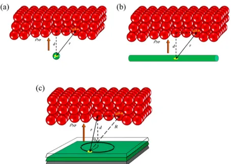
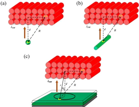
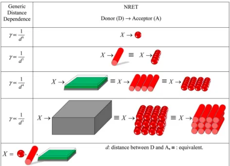
Assuming that the donor size is smaller than the separation distance between the D–A pair and using the long distance approximation, the energy transfer rate ca; i from the donor

Methods: Eighty human serum samples were analyzed with Architect 25-OH D vitamin kit (Abbott Diagnostics, Lake Forest, IL, USA) and LC-MS/MS systems (Zivak Technology,

These thresholds are used by the client to produce feedback information to the server asking to change the rate of the multimedia flow to prevent buffer overflow and

Decrees having force of law as an institution is a delegated legislation of the executive .But it is different in Anglo-Saxon law because in United Kingdom legislative

Sunulan yapıların parametrelerini ö˘grenmek için Üstel Gradyan (ÜD) ve Olasılıksal Bayır ˙Inme (OB˙I) merkezli çevrimiçi ö˘grenme algoritmaları sunulmaktadır..

However, different periodic signals (e.g., sinusoidal signals) may also be used as dither signal. The effect of dither on systems not in the Lur’e form may also be analyzed.