Functionalization of BN honeycomb structure by adsorption and substitution of foreign atoms
C. Ataca and S. Ciraci*Department of Physics, Bilkent University, Ankara 06800, Turkey
and UNAM-Institute of Materials Science and Nanotechnology, Bilkent University, Ankara 06800, Turkey
共Received 4 January 2010; revised manuscript received 3 September 2010; published 1 October 2010兲
We carried out first-principles calculations within density-functional theory to investigate the structural,
electronic, and magnetic properties of boron-nitride 共BN兲 honeycomb structure functionalized by adatom
adsorption, as well as by the substitution of foreign atoms for B and N atoms. For periodic high-density coverage, most of 3d transition metal atoms and some of group 3A, 4A, and 6A elements are adsorbed with significant binding energy and modify the electronic structure of bare BN monolayer. While bare BN mono-layer is nonmagnetic, wide band-gap semiconductor, at high coverage of specific adatoms it can achieve magnetic metallic, even half-metallic ground states. At low coverage, the bands associated with adsorbed atoms are flat and the band structure of parent BN is not affected significantly. Therefore, adatoms and substitution of foreign atoms at low coverage are taken to be the representative of impurity atoms yielding localized states in the band gap and resonance states in the band continua. Notably, the substitution of C for B and N yield donorlike and acceptorlike magnetic states in the band gap. Localized impurity states occurring in the gap give rise to interesting properties for electronic and optical application of the single-layer BN honeycomb structure.
DOI:10.1103/PhysRevB.82.165402 PACS number共s兲: 73.22.⫺f, 73.90.⫹f, 75.50.Pp, 75.75.⫺c
I. INTRODUCTION
Research on BN-based materials have grown gradually in recent years.1–5This is not only due to their fascinating
prop-erties, such as hardness, high melting point, and large band gap, but also due to the geometric similarity of planar, two-dimensional 共2D兲 BN to graphene. Scientists already achieved the synthesis of single-layer BN honeycomb struc-ture on substrates6,7 and a few layer thick structures from
three-dimensional 共3D兲 hexagonal BN either on a substrate or freestanding.8–10 Recently, Jin et al.11 reported the
fabri-cation of freestanding BN honeycomb structure 共we specify it simply as 2D BN throughout the text兲. The realization of the synthesis of 2D BN is rapidly attracting interest on BN, since it has 2D hexagonal lattice, which is commensurate to the lattice structure of covalently bonded graphene. More recently, the synthesis of single-layer composite structures consisting of adjacent 2D BN and graphene domains is realized.12However, unlike semimetallic graphene, 2D BN is
a nonmagnetic, wide band-gap semiconductor with an indi-rect energy gap of 4.64 eV共Ref.13兲 calculated within gen-eralized gradient approximation共GGA兲. The indirect gap is further corrected to 6.82 eV with GW0 self-energy method by Şahin et al.14A theoretical comparative study of 3D and
2D BN, and its nanoribbons comprising their mechanical, electronic, and magnetic properties was reported by Topsakal
et al.132D BN, and their nanoribbons can be easily
function-alized by many different ways for different purposes such as doping,15–17 exchange of atoms and vacancies.18,19
In this paper, using state-of-the-art first-principles plane-wave calculations we investigate the effects of adatoms ad-sorbed on 2D BN, as well as the substitution of foreign at-oms for B and N atat-oms in the honeycomb structure. We consider both high coverage 共where the coupling between adjacent foreign atoms is substantial兲 and low coverage 共where the coupling is negligible兲. We conclude that at high coverage共or decoration兲 of specific adatoms one can turn the
nonmagnetic, wide band-gap material into magnetic, metal-lic, or even half-metallic states. At low coverage, adatoms give rise to localized states in the band gap.
II. METHOD
We perform first-principles, spin-polarized plane-wave calculations20,21 within density-functional theory22 using
projector-augmented-wave potentials.23 The
exchange-correlation potential is approximated by GGA.24For the par-tial occupancies, we use the Methfessel-Paxton smearing method.25 The width of the smearing for all structures is
chosen as 0.01 eV for geometry relaxations and band-structure calculations. For accurate density-of-states 共DOS兲 calculations the width of smearing is taken as 0.1 eV. We consider a single adatom adsorbed to each 共2⫻2兲 and 共4⫻4兲 supercells of 2D BN structure and treat the system using periodic boundary conditions. For high coverage cor-responding to ⌰=1/8, 共2⫻2兲 supercell is used, while low coverage, ⌰=1/32, is treated by using 共4⫻4兲 supercell. A large spacing 共at least ⬃14 Å兲 between adjacent 2D BN layers is taken to prevent interlayer interactions. The number of plane waves used in expanding Bloch functions and k points used in sampling the Brillouin zone 共BZ兲 are deter-mined by a series of convergence tests. In the self-consistent potential and the total energy calculations, the BZ is sampled by 共15⫻15⫻1兲 mesh points in k space within Monkhorst-Pack scheme26 for the 共2⫻2兲 supercells. For calculations
involving共4⫻4兲 supercells, the number of k points is taken as共9⫻9⫻1兲. For accurate DOS calculations, k-points sam-plings are further increased to 共25⫻25⫻1兲 and 共15⫻15 ⫻1兲 for the 共2⫻2兲 and 共4⫻4兲 supercells, respectively. A plane-wave-basis set with the kinetic energy cutoff ប2兩k
+ G兩2/2m=520 eV is used. All the atomic positions and
lat-tice constants are optimized by using the conjugate gradient method, where the total energy and the atomic forces are minimized. The convergence is achieved when the difference
of the total energies of last two consecutive steps is less than 10−5 eV and the maximum force allowed on each atom is
0.03 eV/Å. The pressure on the system is kept smaller than ⬃1 kBar per unit cell in all of the calculations. As a rule, the structure becomes more energetic as its total energy is low-ered. Charge-transfer values are calculated according to the Bader analysis.27
III. ADSORPTION
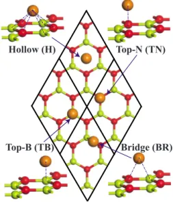
The lowest energy sites of various adsorbed atoms are determined by placing foreign atoms initially to four possible adsorption sites at a height of ⬃2 Å from BN plane as de-scribed in Fig. 1. Upon fully self-consistent geometry opti-mizations with both spin-polarized and spin-unpolarized configurations, where all atoms in the supercell are relaxed in all directions, we determine the equilibrium site as the lowest energy configuration among four different sites. The binding energy of an adsorbed adatom is defined as Eb
= EBN+ EA− EBN+A, where EBNis the total energy of bare 2D
BN, EA is the total energy of free adatom calculated in the
vacuum. EBN+A is the total energy of 2D BN structure with
adsorbed adatom. We investigated the adsorption of follow-ing sfollow-ingle adatoms, namely Sc, Ti, V, Cr, Mn, Fe, Mo, W, Pt, H, C, Si, B, N, O, Ca, Cu, Pd, Ni, and Zn. Among these atoms, Cr, Mn, Mo, W, H, N, Ca, and Zn cannot bind to 2D BN.
A. Adsorption of adatoms to (2Ã 2) BN supercell (Θ = 1 Õ 8) The electronic and magnetic properties of 2D BN are modified through adatom adsorption at high coverage. The
adatom-adatom distance is⬃5 Å at ⌰=1/8, where the mag-netic coupling may be crucial in determining the ground state. In order to account for the antiferromagnetic 共AFM兲 coupling between adatoms and to allow their reconstruction we treated ⌰=1/8 coverage in 共4⫻4兲 supercell, which in-cludes four 共2⫻2兲 supercells each having a single adatom. This way adatom-adatom distance of ⬃5 Å is maintained. We further carried out geometry relaxation with three differ-ent initial magnetic ordering of adatoms. First case is where adatoms are coupled antiferromagnetically. The second case is similar to first one but adatoms are initially coupled ferro-magnetically 共FM兲. The last case corresponds to a spin-unpolarized, nonmagnetic 共NM兲, geometry relaxation. Our calculations indicate that Cu, Ni, Pd, and Pt adatoms have nonmagnetic ground state for⌰=1/8, whereas Sc, Ti, and V have AFM ground state. Oxygen is the only adatom which is found to be in the FM ground state. Boron and carbon ada-toms undergo a reconstruction to lower the total energy in 共4⫻4兲 supercell at ⌰=1/8. Among all adatoms, Si and Fe present the most interesting situation, where 2D BN mono-layer is changed to half-metallic state. However, these ada-toms have small binding energies and thus are excluded from our further analysis. Also Cu having a binding energy smaller than 0.25 eV is also excluded from our study. Our results are given in Table I. In Fig.2, the calculated energy band structures and corresponding total density of states 共TDOS兲 and partial density of states 共PDOS兲 of Ni, Pd, or Pt adatom+ 2D BN system are presented. The band structure of bare 2D BN folded to共2⫻2兲 BZ is also presented to reveal the effect of the adatom adsorption on the electronic struc-ture.
Nickel atom with 4s2+ 3d8electronic configuration is
ad-sorbed at TN site. Even if Ni atom is placed at H or BR sites, it eventually moves to TN site. Flat bands slightly below the Fermi energy are all derived from the 3d orbitals of Ni atom. The band above the Fermi level is mainly formed from the combination of 4s and 3dz2 orbitals of Ni. Accordingly, the
band structure of parent BN layer is not distorted consider-ably. The charge transfer between Ni and 2D BN is relatively small and does not cause any significant dipole moment.
Adsorption of Pd and Pt give rise to electronic and mag-netic properties similar to those of adsorbed Ni. They are adsorbed also at TN site and have high binding energies. Since the radius of Pd and Pt are relatively larger than Ni, the distance to the nearest N atom of 2D BN, dN is slightly
larger. The charge transfer between 2D BN and the adatom is small. Ni, Pd, and Pt have ionization energies of 7.63 eV, 8.33 eV, and 8.96 eV, respectively.28 This ordering of the
ionization energies complies with the ordering of work func-tion,⌽, of Ni, Pd, and Pt covered 2D BN. For both Pd and Pt, the bands slightly below the Fermi level are all derived from localized d orbitals but the band above Fermi level is mainly formed from s orbital of adatom with some dz2
con-tribution similar with the case in Ni adsorption. Even if Pd and Pt have the same indirect band gap energy, Pd shows more dispersive band slightly above the Fermi level.
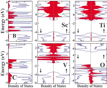
TDOS and PDOS corresponding to ⌰=1/8 coverage of B, C 关which undergo a reconstruction in 共4⫻4兲 supercell兴; Sc, Ti, V共which have AFM ground state兲, and O 共which has FM ground state兲 are presented in Fig. 3. Four carbon
Hollow (H) Top-N (TN)
Bridge (BR) Top-B (TB)
FIG. 1.共Color online兲 A 共4⫻4兲 supercell of 2D BN honeycomb
structure, which consists of four共2⫻2兲 supercells. Various possible
adsorption sites of adatoms are indicated. The hollow site, H: the
adatom共gray/orange ball兲 is placed on top of the center of a
hexa-gon. TN site: the adatom is placed on top of nitrogen共dark gray/
red兲. TB site: the adatom is placed on top of boron 共light gray/
green兲. The bridge site BR: the adatom is located on top of the
adatoms treated in a 共4⫻4兲 supercell undergo a reconstruction;29 while three C atoms are adsorbed near TN
sites, the remaining one is moved to the BR site. Upon re-construction, the charge on C adatom at the bridge cite is minute positive, whereas those at TN site are negatively charged by ⬃0.6. Carbon adatoms at TN site take their charge mostly from the nearest N atom. The bonding of C at TN cite has an ionic character resulting a dipole moment on the system.
Sc, Ti, and V have AFM ground state at⌰=1/8.30Unlike
Sc and Ti, adsorption of V does not make the system metal-lic. The energy bands below the Fermi level is mainly from
dxy, dyz, dxz and above the Fermi level is mainly from dx2
and dz2. The energy band gap of 0.19 eV originates from the
splitting of 3d orbital states.
Among all adatoms in Table I, only O has FM ground state and is absorbed at TB site. The excess charge on the
TABLE I. Calculated structural, electronic, and magnetic properties of 2D BN monolayer at uniform⌰=1/8 adatom coverage.
Equi-librium positions of the adatoms, such as TN, TB, H, and BR are described in Fig. 1; distances of adatom to the nearest N, dN 共in Å兲;
distances of adatom to the nearest B, dB共in Å兲; the height of adatom from the BN plane, h 共in Å兲; the average B-N bond length, dBN共in
Å兲; the binding energy of adatom, Eb共in eV兲; and the net magnetic moment per supercell, 共in B兲. Electronic structure is specified as
metallic共M兲 or semiconductor 共SC兲. The type of the band gap can be either direct 共dr兲 or indirect gap 共id兲. The energy gap of the system
after adsorption, Eg共in eV兲; the transfer of charge to the adatom from BN, ⌬ 共in electrons and ⌬⬍0, if adatom is negatively charged兲; the
dipole moment of the system along the z–direction, p共in eÅ兲; and work function 共or photoelectric threshold for semiconductors兲 is ⌽ 共in
eV兲. For the adatoms, which have either NM or FM ground states, calculations are performed using 共2⫻2兲 supercell; whereas for adatoms,
which have either AFM ground state or reconstruction,共4⫻4兲 supercell are used with ⌰=1/8. For adatoms undergoing a reconstruction, ⌬
is given for the average charge transfer per adatom.
Magnetic ground state Adatom Position dN dB h dBN Eb Electronic structure Gap type Eg ⌬ p ⌽
NM Ni TN 1.87 2.31 1.84 1.46 1.14 SC dr 0.43 0.17 −0.18 3.91 Pd TN 2.15 2.57 2.12 1.46 0.94 SC id 0.93 0.02 −0.15 4.41 Pt TN 2.04 2.49 2.04 1.46 1.48 SC id 0.93 −0.03 −0.10 4.66 FM O TB 2.33 1.47 1.76 1.46 0.98 2.00 SC id 0.05 −0.64 0.24 7.02 AFM Sc H 2.49 2.54 2.03 1.46 0.90 0.00 M 0.67 0.30 3.03 Ti H 2.44 2.48 1.99 1.45 0.92 0.00 M 0.52 0.98 3.56 V TN 2.21 2.67 2.26 1.45 0.60 0.00 SC id 0.19 0.36 0.04 2.81 NM共Reconstruction兲 B TN 1.61 1.98 1.58 1.46 0.80 SC id 0.64 0.40 1.09 5.45 C BR+ TN 1.52 1.66 1.28 1.46 1.38 SC dr 0.35 −0.45 0.54 5.74 Ni Pt Pd -6 -4 -2 0 2 4 6 Μ Γ Κ Μ Density (states/eV) 0 2 4 -4 -2 0 2 4 6 Energy (eV) Μ Γ Κ Μ Density (states/eV) 0 2 4 -6 -4 -2 0 2 4 6 Μ Γ Κ Μ Density (states/eV) 0 2 4 -6 -6 -4 -2 0 2 4 6 Energy (eV) Μ Γ Κ Μ EF EF BN Density (states/eV) 0 2 4 EF (a) (b) (c) (d) EF
FIG. 2. 共Color online兲 共a兲 The energy band structure of bare 2D
BN folded to the共2⫻2兲 supercell and corresponding TDOS. Zero
of band energy is set at the Fermi energy, EF.共b兲–共d兲 The energy
band structure of single Ni, Pd, and Pt adsorbed to each 共2⫻2兲
supercell of 2D BN 共⌰=1/8兲. Corresponding TDOS 共continuous
black/blue line兲 and PDOS projected to the adatom 共shaded dark/
red兲 are also indicated. The energy gap of semiconductors are
shaded共light/yellow兲. The ground states are nonmagnetic.
Sc
Ti
-6 -4 -2 0 2 -6 -4 -2 0 2 -6 -4 -2 0 2 -4 -2 0 2 4 6V
O
Density of States Density of States Density of States -4 -2 0 2 4
Energy
(eV
)
C
-4 -2 0 2 4Energy
(eV
)
B
FIG. 3. 共Color online兲 TDOS 共dark/blue line兲 and PDOS
共shaded gray/red兲 for B, C, O, Sc, Ti, and V adatoms at high
cov-erage,⌰=1/8. Up 共down兲 arrow on the right 共left兲 site of TDOS
and PDOS indicates spin direction. Zero of the DOS energy is set to
the Fermi energy, EFof the adatom+ 2D BN system which is
indi-cated with dashed-dotted gray/green line. All adatoms treated in 共4⫻4兲 supercell to allow antiferromagnetic interaction or
recon-struction, whereby single adatom is adsorbed to each共2⫻2兲
super-cells of 共4⫻4兲 supercell amounting ⌰=1/8. Sc, Ti, and V have
antiferromagnetic ground state; O has ferromagnetic state; and B and C are nonmagnetic. The state densities are given in arbitrary units but have the same scale for all adatoms.
adsorbed O is transferred from three nearest N atoms, which leads to an ionic character in bonding. Since underlying B atom is positively charged and O is negatively charged, ad-sorbed O pulls the nearest B atom and causes distortion on planar 2D BN monolayer.
B. Adsorption of adatoms to (4Ã 4) BN supercell (Θ = 1 Õ 32) We next investigate the adsorption of a single adatom to 共4⫻4兲 supercell, which corresponds to low density cover-age,⌰=1/32. As indicated in Fig.1, we initially placed the adatoms at four different positions and relaxed their geomet-ric structure with both spin-polarized and spin-unpolarized calculations. Interestingly, we observe that among nine dif-ferent adatoms, the adsorption sites of B, C, and O differ by going from ⌰=1/8 to ⌰=1/32. Since the adatom-adatom distance between adjacent supercells is ⬃10 Å, it can nor-mally be contemplated that the coupling between adatoms are negligible. To verify this assumption, we carried out binding energy calculations for C, O, Ti, Sc, and Pt adatoms in 共8⫻8兲 supercell corresponding to a coverage of ⌰ = 1/128. In Table II we compared the equilibrium binding sites and binding energies, and magnetic states of these at-oms for three different coverage⌰=1/8, 1/32, and 1/128.
The binding energies as well as the magnetic ground states of C, O, Sc, and Ti vary substantially by going from ⌰=1/8 to ⌰=1/32. For C and O, the adsorption sites are also changed. However the situation is not the same when the coverage is further lowered from⌰=1/32 to ⌰=1/128 hence when the adatom-adatom distance is increased from ⬃10 Å to ⬃20 Å. For adatoms included in Table II, the binding energies and magnetic moments are not changing significantly, and the adsorption sites are remaining the same by going from ⌰=1/32 to ⌰=1/128. This finding is cor-roborating our arguments made at the beginning of the paper, that the properties calculated for ⌰=1/32 coverage 关or the adsorption of a single adatom adsorbed to each 共4⫻4兲 su-percell兴 can mimic the adsorption of single isolated adatom on a very large area of 2D BN共or very large adatom-adatom distance兲. Consequently, the bands of adatom+2D BN
calcu-lated at⌰=1/32 become rather flat and can be taken as the localized impurity state 共or resonances if 2D BN states are significantly contributed兲. Under these circumstances, the band gap and the edges of valence and conduction bands can be unaltered. In TableIII, we include the calculated geomet-ric, electronic and magnetic properties of a single adatom adsorbed to 2D BN at ⌰=1/32. The energies of localized and resonance states relative to 2D BN’s valence band edge are also tabulated.
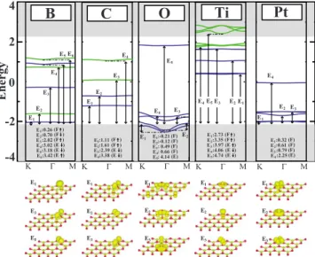
Boron adsorbed on 2D BN on 共4⫻4兲 supercell exhibits electronic, magnetic, and structural properties, which are sig-nificantly different from those of ⌰=1/8. For example, B atom of the planar BN rises ⬃0.2 Å; this slightly changes the sp2-hybridization locally. Two spin-up bands and one
spin-down band are filled below the Fermi energy. In Fig.4, the band structure of B + 2D BN and isosurfaces of charge density corresponding to the localized states E1, E3, and E5
are shown. The magnetic properties are different from the case at ⌰=1/8 since reconstruction of B adatoms does not take place due to the absence of adatom-adatom interaction. Adsorption of C on 共4⫻4兲 supercell of 2D BN causes significant splitting of degenerate p orbital levels. Spin-up and spin-down bands indicated in Fig. 4 originate from px
共E1 state兲 and py 共E2 state兲 orbitals of adsorbed C atom. In
this low coverage, C adatom is adsorbed to BR position, but closer to N atom. Similar to B, the magnetic properties of the C + BN system changed from NM to FM upon lowering the coverage density.
At ⌰=1/8, O adatom creates a surface distortion and pulls underlying B atom upwards. However at ⌰=1/32, O adsorbed at BR site does not generate a distorted BN region. The bands near the edge of valence band have significant dispersion due to strong coupling between O and 2D BN. The AFM ground states of Sc, Ti, and V adsorbed 2D BN at ⌰=1/8 change to FM ground states at ⌰=1/32. Among all adatoms studied in the present paper, electronic and magnetic properties of Ni, Pd, and Pt are not affected upon lowering the coverage density.
Next we address the question whether adsorbed adatom migrates on 2D BN honeycomb structure. Here we consider
TABLE II. Binding energies共Eb兲, magnetic moments 共兲, adsorption sites, and average adatom-adatom
distances共Ref.31兲 共d¯A−A兲 of C, O, Sc, Ti, and Pt adatoms adsorbed on 2D BN at different coverages.
⌰ C O Sc Ti Pt 1/8 Eb共eV兲 1.38 0.98 0.90 0.92 1.48 共B兲 2.00 0.00 0.00 d ¯ A−A=⬃5 Å Site BR+ TN TB H H TN 1/32 Eb共eV兲 1.17 2.01 0.43 0.74 1.52 共B兲 2.00 3.00 4.00 d ¯ A−A=⬃10 Å Site BR BR H H TN 1/128 Eb共eV兲 1.15 1.98 0.37 0.70 1.47 共B兲 2.00 3.00 4.00 d ¯ A−A=⬃20 Å Site BR BR H H TN
only single C and Ti atoms as prototypes and calculate the energy barrier for their motion along the symmetry directions of 2D BN. In Fig.5, the variation in energy of single C and Ti adatoms along symmetry directions are presented. The potential barrier on the migration path for C adatom is ⬃0.30 eV. In the case of Ti the energy barrier on the pos-sible migration path is only 0.15 eV. The latter barrier is not high enough to prevent Ti atoms from cluster formation at elevated temperatures.
IV. SUBSTITUTION (Θ = 1Õ 32)
We, finally deal with the substitutional doping of the spe-cific atoms. Here we consider that Al, Be, and C substitution for B atom; C, O, and P substitution for N atom of 2D BN honeycomb structure. We mimic the substitutional doping by a model, where a specific atom substitutes for a single B or N in every 共4⫻4兲 supercell of 2D BN. In this model the dis-tance between impurity atoms is⬃10 Å resulting in negli-gible coupling between them. The substitution energy Es is
calculated32,33as
Es=
N − 1
N EBN+ EA− EB∨N− EBNS,
Here N is the number of atoms in the supercell, which is
N = 32 for共4⫻4兲 supercell. EBNis the calculated total energy
of 2D BN of the 共4⫻4兲 supercell corresponding to 16 B-N atom pairs. EA is the experimental cohesive energy28 of the
impurity atom in its equilibrium crystal. EBNS is the total
energy of the supercell after substitution process. EB∨Nis the
cohesive energy of either B or N that depends on which atom is exchanged. The experimental cohesive energy of B is de-fined with respect to the B crystal.28However, in the case of
N, the cohesive energy of N is calculated relative to N2in the
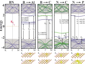
gas phase. According to this expression, a positive energy value means the exchange of foreign adatom either with B or N is endothermic reaction, whereas the negative value indi-cates an exothermic process. Structural relaxations and the lowest energy states of the final structures are further tested with three different initial magnetic moment distributions on the atoms and all these cases are converged to the same values given in TableIV. Here the substitution of C atom for B 共N兲 is of particular interest, since it dopes the 2D BN honeycomb structure as donor共acceptor兲.
We now examine the electronic and magnetic structure of 2D BN substituted by Al, C, and P described schematically in Fig. 6. Al substituting for B and being in the same group with B, but having a relatively large atomic radius, distorts the planar structure of BN layer and is located at a position 0.52 Å higher than the substituted B atom. The valence band of the BN layer does not influence much upon substitution, but states derived from p orbitals of Al adatom appear near the conduction band edge. In Fig. 6, pz orbitals of Al are
dominant in E1 state, however py is the most contributed in
E2 state. In the case of C substituting B, the valence and conduction bands of BN layer are not influenced, except minute splitting between the spin-up and spin-down states resulting from the magnetic C atom. The excess electron of the substituted C atom relative to B leads spin-polarization and fills the E1 state in Fig. 6 like a n-type semiconductor. When substitute for N, C atom creates electron deficiency; states derived from p orbitals of C atom are located near the
TABLE III. Calculated values for single adatom adsorbed to each共4⫻4兲 supercell, corresponding to the coverage ⌰=1/32. Adsorption
site, binding energy, Eb; magnetic moment per共4⫻4兲 supercell,; the distance from 2D BN monolayer, h; the distance from the nearest N
atom, dN; the distance from the nearest B atom, dB; charge transfer,⌬; and energies of relevant localized or resonance states measured from
the top of the valence band, En.共F↑兲 indicates that the corresponding spin-up state is full. 共E↓兲 represents an unoccupied spin-down state.
If no spin direction is indicated, that state is nonmagnetic. R is resonance state having significant contribution from 2D BN states in the band continua. Adsorption site of the adatoms corresponding to their lowest total energy are indicated by TN, TB, BR, or H as described in
Fig.1. Site Ni Pd Pt C Sc Ti V B O TN TN TN BR H H TN BR BR Eb共eV兲 1.15 0.96 1.52 1.17 0.43 0.74 0.58 0.79 2.01 共B兲 2.00 3.00 4.00 5.00 1.00 h共Å兲 1.87 2.15 2.14 1.71 2.08 2.04 2.28 1.83 1.56 dN共Å兲 1.86 2.14 2.02 1.59 2.51 2.46 2.21 1.63 1.52 dB共Å兲 2.31 2.56 2.50 1.77 2.53 2.49 2.66 1.79 1.48 ⌬ 0.16 0.01 −0.01 −0.23 0.59 0.42 0.29 0.30 −0.81 E1 1.43共F兲 0.65共F兲 0.32共F兲 1.11共F↑兲 2.72共F↑兲 2.73共F↑兲 2.16共F↑兲 0.26共F↑兲 −0.21共FR兲 E2 1.83共F兲 0.92共F兲 0.61共F兲 1.61共F↑兲 3.14共F↑兲 3.35共F↑兲 2.57共F↑兲 0.70共F↓兲 −0.12共FR兲
E3 2.80共E兲 1.18共F兲 0.79共F兲 2.39共E↓兲 3.75共E↓兲 3.97共E↑兲 3.01共F↑兲 2.02共F↑兲 0.49共FR兲
E4 4.49共ER兲 2.95共E兲 2.25共E兲 3.38共E↓兲 3.77共E↑兲 4.06共E↓兲 3.48共E↑兲 3.02共E↓兲 0.66共FR兲
E5 3.96共E↓兲 4.74共E↓兲 3.88共E↓兲 3.18共E↓兲 4.14共ER兲
E6 4.01共E↑兲 4.32共E↓兲 3.42共E↑兲
edge of the valence band like a p-type semiconductor. pz
orbital of C splits and spin-up 共E3 state in Fig.6兲 becomes occupied. Because of this unpaired electron C atom attains net 1 B total magnetic moment in both n-type and p-type
substitutional dopings.
Substituted P having relatively larger atomic radius, gives rise to the local deformation and raises 1.42 Å above the plane of 2D BN honeycomb structure. This gives rise to a local dehybridization of planar sp2bonding. Since the upper
valence bands of parent 2D BN are derived mainly from nitrogen atoms, these bands are affected upon their exchange with foreign atoms. Hence several resonances appear, such as E1 and E2 in the upper part of valence band when P
substitutes for N atom in Fig.6. In addition a localized state E3occurs near the conduction band edge.
V. DISCUSSION AND CONCLUSIONS
In this paper, we showed that 2D BN can be functional-ized to attain properties, which can be useful in future appli-cations in nanoelectronics and nanomagnetics. Functional-ization can be achieved either through the adsorption of foreign atoms at different coverage or substitution of foreign atoms for B or N in honeycomb structure. We considered a number of foreign atoms, such as Sc, Ti, V, Cr, Mn, Fe, Mo, W, Pt, H, C, Si, B, N, O, Ca, Cu, Pd, Ni, and Zn. Part of
these atoms are bound with a significant energy and form chemical bonds with 2D BN. Cu, Fe, and Si have binding energy smaller than 0.25 eV, but Cr, Mn, Mo, W, H, N, Ca, and Zn cannot bind to 2D BN. Owing to the van der Waals interaction, the true binding energies can be 0.1–0.2 eV larger than those calculated with GGA in the present work.
High coverage of adatoms corresponding to⌰=1/8 leads to dramatic modifications in electronic structure, if the re-lated binding energy is significant. Under these circum-stances, either the wide band gap of 2D BN can be reduced or diminished and the system becomes metallic. Under cer-tain circumstances, the nonmagnetic 2D BN atcer-tains magnetic moment. Ni, Pd, and Pt covered 2D BN are nonmagnetic semiconductors with band gap relatively smaller than that of the parent 2D BN. Sc, Ti forming a 共2⫻2兲 structure on 2D BN are AFM metals, V + 2D BN is an AFM semiconductor. Remarkably, B+ and C + 2D BN undergo a 共4⫻4兲 recon-struction and have a band gap smaller than the parent 2D BN. Oxygen covered 2D BN is found to be a FM, small band gap semiconductor, which may display high spin polarization under bias voltage. If the interaction between adatom and 2D BN is weak, the electronic structure can be viewed as the E1 E3 E5 Energy -2 -4 4 2 0 Γ Κ Μ Γ Κ Μ Κ Γ Μ Κ Γ Μ Κ Γ Μ
B
C
O
Ti
Pt
E1 E2 E3 E1 E2 E3 E1 E2 E3 E1 E2 E3 :0.26 :0.70 :2.02 E1 E2 E3 E1 E2 E3 E4 E5E6 :3.02 :3.18 :3.42 E4 E5 E6 E1 E2 E3 E4 :1.11 :1.61 :2.39 E1 E2 E3 :3.38 E4 E1 E2 E3 E4E5 :2.73 :3.35 :3.97 E1 E2 E3 :4.06 :4.74 E4 E5 E1 E2E3 E4 :0.32 :0.61 :0.79 E1 E2 E3 :2.25 E4 :-0.21 :-0.12 : 0.49 E1 E2 E3 : 0.66 : 4.14 E4 E5 (F) (F) (F ) (F ) (F ) (E ) (E ) (E ) (F ) (F ) (E ) (E ) (F ) (F ) (E ) (E ) (E ) (F) (E) (F) (F) (F) (F) (E) E1 E2 E3 E4 E5FIG. 4. 共Color online兲 Schematic of the relevant energy levels
共or bands兲 of adatom 共B, C, O, Ti, and Pt兲 adsorbed to 共4⫻4兲 supercell of the single layer BN. The light/gray shaded region in the background is the valence and conduction band region of 2D BN. Zero of band energy is set at the Fermi level of the parent, bare 2D
BN, EF. Spin-up and spin-down bands are shown by dark/blue and
light/green lines, respectively. Solid bands indicates that the contri-bution of adatom to the band is more than 50% except O adatom.
Energies of some of the relevant adatom共impurity兲 states relative to
valence band edge of parent 2D BN are indicated. Below each energy diagram of adatoms, charge density isosurfaces of specific
states are shown. The isosurface value is taken as 7
⫻10−5 electrons/Å3.共Note that all localized states of O have
sig-nificant contributions from BN states and are shown by solid dark/
blue lines.兲 0 0.2 1.0 0.4 0.6 0.8 H H TB TN BR 1.00 eV 0.76 eV 0.04 eV 0.07 eV H TN BR Energy Differ ence (eV)
C
H TB TN 0.30 eV 0.19 eV 0.22 eV H 0 0.2 0.1 0.3 Position Energy Differ ence (eV) BR BR H TBTi
FIG. 5. 共Color online兲 Variation in energy of a single C and Ti
adatom as they are moving along special directions of a hexagon of 2D BN honeycomb structure. The possible migration path of ad-atom facing minimum energy barrier is shown by stars on the
combination of electronic band structure of 2D BN mono-layer and adatom monomono-layer. Si and Fe are weakly bound to 2D BN and change the wide band gap of 2D BN to a half-metal.
At low coverage corresponding to⌰=1/32, the large dis-tance between adatoms hinders any significant interaction between them. This situation is taken to mimic a single, iso-lated atom adsorption to 2D BN, which gives rise to local-ized states in the wide band gap of 2D BN honeycomb struc-ture. This conjecture is confirmed by examining the adsorption of single C, O, Sc, Ti, and Pt to共8⫻8兲 supercell resulting in⬃20 Å adatom-adatom distance. In this respect, the adsorbed adatoms at⌰=1/32 act as dopants of 2D BN. In a few cases the adsorption site and magnetic state undergo a change by going from the high, ⌰=1/8 to low coverage, ⌰=1/32.
Not only adatoms, but also substitution of foreign atoms for B or N in the honeycomb structure give rise to localized impurity states in the gap, which attribute interesting elec-tronic properties to the system. In particular, the substitution of C for B yields an excess charge and gives rise to two donor states near the edge of conduction band, the lower lying spin-up band being full. In contrast, the substitution of C for N yields a single-electron deficiency and gives rise to two acceptor states above the top of valence band, the lower lying spin-up state being full. In both cases, the unpaired spins of C atom give rise to magnetic moment= 1 B.
In conclusion, while 2D BN is a mechanically stiff and nonmagnetic wide band gap semiconductor, its band gap can be engineered through adatom decoration. In specific cases 2D BN attains magnetic properties and becomes metallic. Foreign atoms adsorbing at low coverage or exchanging with B or N atoms give rise to donorlike or acceptorlike states in band gap. At the end, the material achieves interesting prop-erties. Some of these properties can be exploited in future applications.
ACKNOWLEDGMENTS
Part of computational resources have been provided
through a grant共Grant No. 2-024-2007兲 by the National Cen-ter for High Performance Computing, Istanbul Technical University. We thank the DEISA Consortium 共www.dei-sa.eu兲, funded through the EU FP7 under Project No. RI-222919, for support within the DEISA Extreme Computing Initiative. S.C. acknowledges partial support from TUBA, Academy of Science of Turkey. Authors thank Ethem Aktürk for helpful discussions.
TABLE IV. Substitution energy, Es; magnetic moment per共4⫻4兲 supercell,; the height of the
substi-tuting atom from 2D BN monolayer, h; the distance from the nearest B or N atom, dB∨N; charge transferred
to substituting atom共Ref.27兲, ⌬; and energies of relevant localized states in the band gap, En.共F↑兲 indicates
that the corresponding spin-up state is full.共E↓兲 indicates unoccupied spin-down state. If no spin direction is
indicated, that state is nonmagnetic.
B→ N→ Al Be C C O P Es共eV兲 5.47 5.23 5.47 3.42 6.51 3.77 共B兲 NM NM 1.00 1.00 1.00 NM h共Å兲 0.52 0.01 0.01 0.00 0.00 1.42 dB∨N 1.71 1.56 1.41 1.52 1.50 1.88 ⌬ 2.28 1.60 1.15 −1.89 −1.51 −0.47 E1 2.76共E兲 −2.29共F兲 3.50共F↑兲 −1.69共F↑↓兲 −2.45共F↑兲 −0.76共F兲 E2 3.02共E兲 −0.83共F兲 4.22共E↓兲 −0.69共F↑↓兲 −2.16共F↓兲 −0.07共F兲
E3 4.22共E兲 4.38共E兲 0.17共F↑兲 4.20共E兲
E4 6.26共E兲 1.07共E↑兲 EF Γ Κ Μ :2.76 :3.02 :4.22 :4.22 :3.50 : 4.20 : -0.07 : -0.76 : 0.17 :-0.69 : 1.07 Γ Κ Μ Κ Γ Μ Κ Γ Μ Κ Γ Μ Energy 0 2 4 -4 -2 B Al B C N C N P E1 E2 E1 E2 E3 E4 E1 E2 BN E1 E2 E3 E1 E2 E3 E1 E2 E3 E1 E2 E2 E3 E4 E1 E2 E3 E4 E2 E1 E2 E3 (F) (F) (E) (E) (E) (E) (F(F )) (F ) (E ) (E )
FIG. 6. 共Color online兲 Schematic energy-level diagram of Al
and C substituting B; and C and P substituting N in a 共4⫻4兲
su-percell of 2D BN. The light/gray shaded region in the background is the valence and conduction-band continuum of 2D BN. Zero of energy is set to the Fermi level of bare 2D BN. Spin-up bands are indicated with dark/blue lines whereas spin-down bands are light/
green. Thick solid bands共levels兲 are states localized at the
substi-tuted atom and nearest atoms of 2D BN. Thin solid bands stand for the delocalized states. The energies of some of the localized states with respect to the valence band edge are shown in units of eV. Charge density isosurfaces of some of the relevant states are shown below the corresponding band diagram. The isosurface value is
1P. F. McMillan,Nature Mater. 1, 19共2002兲.
2Z. Pan, H. Sun, Y. Zhang, and C. Chen,Phys. Rev. Lett. 102,
055503共2009兲.
3K. Miyoshi, D. H. Buckley, J. J. Pouch, S. A. Alterovitz, and E.
Sliney,Surf. Coat. Technol. 33, 221共1987兲.
4N. G. Chopra, R. J. Luyken, K. Cherrey, V. H. Crespi, M. K.
Cohen, S. G. Louie, and A. Zettl,Science 269, 966共1995兲.
5R. Arenal, M. Kociak, and N. J. Zaluzec,Appl. Phys. Lett. 90,
204105共2007兲.
6W. Auwärter, H. U. Suter, H. Sachdev, and T. Greber, Chem.
Mater. 16, 343共2004兲.
7M. Morscher, M. Corso, T. Greber, and J. Osterwalder,Surf. Sci.
600, 3280共2006兲.
8W. Q. Han, L. Wu, Y. Zhu, K. Watanabe, and T. Taniguchi,Appl.
Phys. Lett. 93, 223103共2008兲.
9D. Pacile, J. C. Meyer, C. O. Girit, and A. Zettl, Appl. Phys.
Lett. 92, 133107共2008兲.
10K. S. Novoselov, D. Jiang, F. Schedin, T. J. Booth, V. V.
Khot-kevich, S. V. Morozov, and A. K. Geim,Proc. Natl. Acad. Sci.
U.S.A. 102, 10451共2005兲.
11C. Jin, F. Lin, K. Suenaga, and S. Iijima,Phys. Rev. Lett. 102,
195505共2009兲.
12L. Ci, L. Song, C. Jin, D. Jariwala, D. Wu, Y. Li, A. Srivastava,
Z. F. Wang, K. Storr, L. Balicas, F. Liu, and P. M. Ajayan,
Nature Mater. 9, 430共2010兲.
13M. Topsakal, E. Aktürk, and S. Ciraci,Phys. Rev. B 79, 115442
共2009兲.
14H. Şahin, S. Cahangirov, M. Topsakal, E. Bekaroglu, E. Aktürk,
R. T. Senger, and S. Ciraci,Phys. Rev. B 80, 155453共2009兲.
15K. Nose, H. Oba, and T. Yoshida,Appl. Phys. Lett. 89, 112124
共2006兲.
16N. S. Venkataramanan, M. Khazaei, R. Sahara, H. Mizuseki, and
Y. Kawazoe,Chem. Phys. 359, 173共2009兲.
17J. Zhang, S. Wang, X. Du, K. Xu, and V. Ji,J. Phys. Chem. C
113, 17745共2009兲.
18A. Zobelli, C. P. Ewels, A. Gloter, and G. Seifert,Phys. Rev. B
75, 094104共2007兲.
19W. Orellana and H. Chacham,Phys. Rev. B 63, 125205共2001兲.
20M. C. Payne, M. P. Teter, D. C. Allen, T. A. Arias, and J. D.
Joannopoulos,Rev. Mod. Phys. 64, 1045共1992兲.
21Numerical computations have been carried out by using VASP
software: G. Kresse and J. Hafner,Phys. Rev. B 47, 558共1993兲;
G. Kresse and J. Furthmüller,ibid. 54, 11169共1996兲.
22W. Kohn and L. J. Sham, Phys. Rev. 140, A1133 共1965兲; P.
Hohenberg and W. Kohn,Phys. Rev. 136, B864共1964兲.
23G. Kresse and D. Joubert,Phys. Rev. B 59, 1758共1999兲.
24J. P. Perdew, J. A. Chevary, S. H. Vosko, K. A. Jackson, M. R.
Pederson, D. J. Singh, and C. Fiolhais,Phys. Rev. B 46, 6671
共1992兲.
25M. Methfessel and A. T. Paxton,Phys. Rev. B 40, 3616共1989兲.
26H. J. Monkhorst and J. D. Pack,Phys. Rev. B 13, 5188共1976兲.
27G. Henkelman, A. Arnaldsson, and H. Jonsson,Comput. Mater.
Sci. 36, 354共2006兲.
28C. Kittel, Introduction to Solid State Physics, 7th ed. 共Wiley,
New York, 1996兲.
29When treated in the共2⫻2兲 supercell at ⌰=1/8, C adatoms
at-tain net magnetic moment of 2 B per 共2⫻2兲 supercell. This
configuration is, however, 0.3 eV per adatom higher
共energeti-cally less favorable兲 than those reconstructed in the 共4⫻4兲
su-percell. Similarly, for ⌰=1/8 B treated in 共2⫻2兲 supercell,
binding at the BR site, attain magnetic moment of 1 B, but
becomes 0.12 eV per adatom less favorable relative to the re-constructed structure.
30The excited state of AFM ground state of Sc, Ti, and V is the FM
state with the magnetic moment of 0.45 B, 3.51 B, and
4.80 B; and with the energies of 30 meV, 50 meV, and 20 meV
above the ground state, respectively.
31The optimized lattice parameters can be different for different
adatoms and for different coverages.
32C. Ling and D. S. Sholl,Phys. Rev. B 80, 214202共2009兲.