High-performance acoustic microscope
Abdullah AtalarElectrical and Electronics Engineering Department, Middle East Technical University, Ankara, Turkey
Martin Hoppe
Ernst Leitz Wetzlar GmbH, Weczlar, West Germany
(Received 14 April 1986; accepted for publication 4 June 1986)
A commercial scanning acoustic microscope operating in the frequency range of 50-2000 MHz is described. It has a stable scan mechanism suitable for the frequency end to give high-resol.ution images and modes to allow for material characterization at the low-frequency end. The high-frequency electronics permitting a wideband operation with a variety of acoustic lenses are described. Microprocessors control many parts of the the instrument to release the user from the routine adjustments, resulting in a user-friendly interface. Images are presented to show the resolution and penetration abilities of the instrument at several frequencies, along with comparative optical images.
INTRODUCTION
The scanning acoustic microscope is finding applications as a powerful instrument for imaging and characterization of materials. 1.2 Research laboratories in countries such as the U.S./-6 Japan,7 England,H France,9 Canada,1O and the U.S.S.R. II have developed their own microscopes for
in-house use, following the guidelines of the Stanford micro-scope. 12, 1'1 These microscopes operate successfully in various
modes at various frequencies. On the other hand, developing a general purpose, versatile, and powerful commercial acoustic microscope poses more difficult problems. A few commercial instruments have shown up recently at the mar-ketplace. In this paper we describe the scanning acoustic microscope (ELSAM) developed at Ernst Leitz Wetzlar GmbH, West Germany,14.15 after a license agreement with Stanford University.
ELSAM is an acoustic microscope combined with an optical microscope capable of generating visual or hard-copy acoustic images. Three microprocessors in communi-cation with each other control many parts of the instrument. The user is released from routine adjustments of the compli-cated system and therefore can concentrate on the applica-tion side through the user-friendJy interface. Use of micro-processors simplifies the hardware and wiring, resulting in a reliable system. In this paper we also present many acoustic images obtained with EJ_SAM which show the capabilities of the scanning acoustic microscope as compared with the optical microscope.
I. DESCRIPTION OF THE ACOUSTIC MICROSCOPE
A thorough description of the scanning acoustic micro-scope and its theoretical performance limits can be found elsewhere. 13.16 Here we will describe the features of the de-veloped microscope which is different from a laboratory-type instrument.
The wavelength ofthe acoustic waves used in imaging is determined by the frequency of operation. To serve both high-resolution and high-penetration depth applications, an acoustic microscope with broad-frequency coverage is
nec-essary. We have selected the 50-2000-MHz frequency band as the operation range. Such a frequency range would cover almost all the requirements. The high-frequency end is need-ed for high-resolution images, whereas the low-frequency end is suitable for high-penetration depth applications. The high-frequency end is limited to 2 GHz, although it is possi-ble to get images at higher frequencies. 17 Above 2 GHz the working distance must be made very small and, consequent-ly, working with such an instrument is extremely difficult. For ease of operation and for compatibility with many ob-jects, the coupling liquid is selected to be water. Acoustic microscopes working with cryogenic liquids IH or pressurized
gases 19 have been demonstrated. They can give higher-reso-lution performance at the given frequency, but they suffer from difficulty of operation.
To get both optical and acoustical information from the same area of the object, a reflected-light microscope is com-bined with the acoustic microscope. The optical microscope is a general-purpose high-performance unit capable of work-ing with many optical lenses under various imagwork-ing modes. The mechanical accuracy of conversion between the two mi-croscopes is such that the obtained images are centered to within a few micrometers of each other.
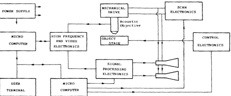
The main sections of the acoustic microscope are its me-chanical parts, its electrical parts, and its acoustic part, as depicted in Fig. 1 in block diagram form. The critical me-chanical parts include the X-Y scan mechanism, the Z ad-justment mechanics, and the object leveling apparatus. The X-Y scan mechanism is able to generate a 1 X 1 mm2 raster scan with less than I-flm deviation in the Z direction. It is an electromechanical scan utilizing electromagnets and long leaf springs. A closed loop control system utilizing optical position sensors is used for scanning operation to provide linearity and to reduce sensitivity against external vibra-tions. The fast scan is done with a sawtooth waveform at a frequency of 30 or 60 Hz (25/50 Hz in Europe), depending on the scan magnitude. Z adjustment can be done either manuaIIy or remotely by an electrical motor. Through re-mote adjustment it is possible to focus the beam to the de-sired object surface as well as to obtain V(z) information. 13 2568 Rev. Sci. Instrum. 57 (10), October 1986 0034-6748/86/102568.()9$O1.30 @ 1986 American Institute of Physics 2568
f - MF.CHANICAL SCAN
POWER SUPPI,Y DRIVE ELECTRONICS
r-+
AcousticObJE'ctivE'
Q
MICRO HIGH FR EQUENCY
OBJECT I CONTROL AND VroEO STAGE COMPUTER ELECTRONICS f:LECTRONICS SIGNAL I. PROCESSING F.LECTRON ICS USER MICRO TERMINAL COMPUTER
FIG. I. Block diagram of the scanning acoustic microscope.
The object-leveling apparatus is coupled to the object stage to adjust the object surface parallel to the X- Y scan surface, and it is necessary to increase the image quality by keeping the same focus position throughout the sample surface.
The microscope electrical parts can be grouped in five major sections: the user terminal, the high-frequency and video electronics, the signal processing. scan, and control electronics, the power supply, and the image display tubes.
The user terminal is a small terminal designed to take commands from the user and send it to the other parts of the microscope for the selected operating mode to act as a con-troller for the acoustic microscope system. It is also used to keep the user up to date on the modes of the microscope. The terminal has a dedicated keyboard and a joystick through which aU the commands and adjustments are easily entered, and a 2-line by 40-character plasma display on which all the relevant information is shown. Through the keyboard. the user can select the various display and signal processing modes, change the magnification, the coupling liquid tem-perature, or the operation frequency. The user terminal is designed around an 8-bit Intel 8085 microprocessor with special drive circuitry for plasma display and other peripher-als for keyboard readout, LED drive, and communication. From an architectural point of view, it is possible in the fu-ture to change the user terminal with a more powerful com-puter, such as a personal computer.
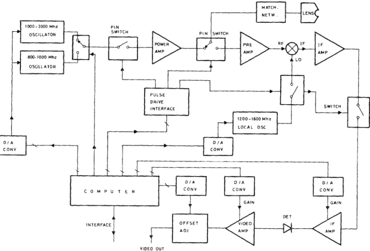
The frequency electronics are composed of high-frequency components to make the microscope operate at the selected frequency. It operates in the weB-known pulse-echo mode. It receives commands from the user terminal and sets its operating point accordingly. The 50-2000-MHz frequency band is divided between two units. A block dia-gram of the high-frequency electronics operating at 0.8-2.0 GHz is shown in Fig. 2. It is basically composed of transmit-ter oscillators, pulse generating circuits, and a superhetransmit-tero- superhetero-dyne receiver. The frequency range is divided between two varactor tuned oscillators (VTO) to generate transmitted signal. The frequency can be adjusted by the varactor vol-tage. This voltage is obtained from a digital-to-analog
con-2569 Rev. ScI. 'nstrum., Vol. 57, No. 10, October 1986
I
I.
vetter driven by a computer. The nonlinear frequency-vol-tage characteristics of the oscillators are stored in a lookup table to generate the correct frequency. The output of the transmitter oscillator is pulsed by a p-i-n diode switch. The switch is capable of generating 10-ns pulses with an on4)jf ratio of more then 80dB. Thep-i-n switch is driven by a pulse drive electronics, again controlled by the computer. The pulsed rf signal is amplified with a solid-state amplifier to a level of 1 W. The signal is fed to one of the arms of a double throw p-i-n switch. The common arm of the switch is con-nected to the acoustic lens element. The acoustic lens is matched to 50-D. impedance level with a proper matching network. The voltage-stan ding-wave ratio (VSWR) is kept below 2 : 1 within the band to keep the magnitude of the undesired reflections down. The second arm of the p-i-n switch goes to a wide-band preamplifier. The pulse drive interface driving this switch is adjusted such that the first arm is connected to the common arm only when the first p-i-n switch is on, and the second arm is connected to common arm at a time slightly after the transmitter pulse is applied to the lens element. This timing assures that the preamplifier is not saturated by the relatively high-amplitude input pulse and its reflections from the acoustic lens matching network. Moreover. the on4)jf ratio of the input pulse is increased to over 100 dB. The output ofthe preamplifier is fed to a wide-band mixer. The local oscillator for the mixer operates in the frequency range 1200--1600 MHz. This range is enough when the intermediate frequency (IF) is selected to be 400 MHz. The local oscillator is also pulsed to keep the IF ampli-fiers far from the saturation by the spurious reflections gen-erated in the acoustic lens element. The local oscillator is turned on only during the time slot the object pulse may appear. The necessary pulse is created by the pulse-drive electronics using computer-controlled digital delay tech-niques. Hence the receiver will function only during a time window selected by the pulse-drive interface. The frequency of the local oscillator is corrected by the microprocessor to maximize the output voltage each time a new frequency is selected. This procedure is necessary because there is a
1000 -2000 Mhz OSCILLATOR BOO·IOOO Mhz OSCJLLATOR PIN SWITCH C O M P U T E R INTERFACE PULSE DRIVE INTERFACE VIDEO OUT OFFSET AOJ PI N SWITCH IZOO-1600Mhz LOCAL OSC
FIG. 2. Block diagram of the high-frequency electronics suitable for 800-2000 MHz and video electronics.
siderable variation on the voltage-frequency characteristics of the individual VTO's. The two IF amplifiers in cascade provide a gain in excess of 80 dB. There is another switch between the two IF amplifiers to further reduce the unde-sired pulses. This switch is kept on in the same time slot as the local oscillator. The gain of the IF amplifier is adjustable by the computer to the desired level. Finally, the output of the IF amplifier is detected by a detector diode to generate a 4O-kHz bandwidth video signal which is proportional to the amplitude ofthe received acoustic signal. The high-frequen-cy electronics section has a dynamic range in excess of 100 dB. The computer responsible for the whole high-frequency electronics is built around an 8-bit single-chip Intel 8749 microprocessor with suitable peripherals.
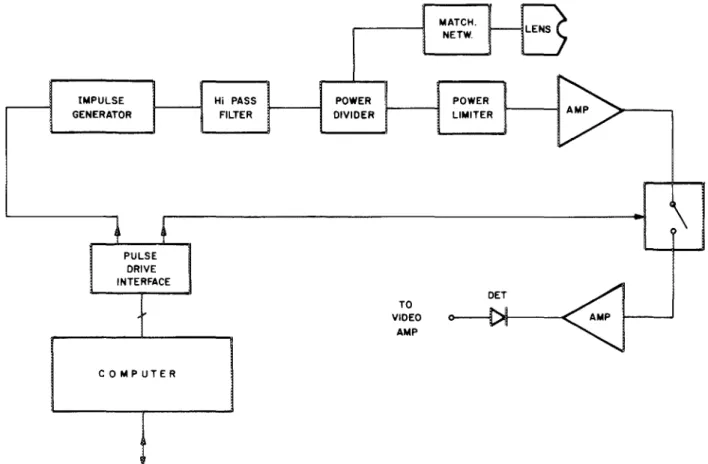
A block diagram of the high-frequency electronics suit-able for the 50-800-MHz range is depicted in Fig. 3. In this frequency range the electronics are relatively simple. be-cause the overall system losses are much smaller, and larger lens diameters provide a greater seperation between spurious and information pulses. A short base-band pulse is used to excite the transducer. A pulse of I-ns duration and 20-V magnitude is utilized which contains frequency components up to 1 GHz. This pulse is fed to the transducer through a power divider. Use of the power divider at this position pro-vides some degree of isolation between the transmitter and the receiver side. A circulator at this position would have been a better choice than the power divider which has a total
2570 Rev. SCi.lnstrum., Vol. 57, No. 10, October 1986
loss of 6 dB, but unfortunately, circulators in such a broad-and low-frequency range are not available. The output of the power divider is connected to a limiter to protect the input of the receiver amplifier. After 40-dB amplification a mixer is used as a switch to gate out the unwanted parts of the incom-ing pulse train. After the time-gatincom-ing operation a further amplification of 40 dB is performed. High-pass filters are placed in the receiving chain to get rid of switching spikes caused by the time gating operation. The amplitUde detec-tion of the amplifier output provides the necessary video sig-nal for further processing.
The video electronics takes the video signal obtained from the high-frequency electronics section as the input. It is controlled by the same computer controlling the high-fre-quencyelectronics. Its basic functions are to shift the dc level of the video signal and to change the video gain. Those vari-ables can be adjusted by the user with the joystick on the user terminal.
The signal processing electronics is responsible for mak-ing some simple signal processmak-ing functions, such as invert-ing the video signal to get reverse video images or differenti-ating it to get emphasized edges in the images. It is also possible to add the video signal to its derivative with a con-trollable ratio to get the desired image improvement. The video gain can be adjusted either automatically or manually. This section is controlled by the third computer of the acous-tic microscope system. The commands sent by the user
r -______
~_M_A_T_C_H_. ~----BENS
_ NETW. IMPULSE GENERATOR Hi PASS FILTER POWER DIVIDER POWER LIMITER PULSE DRIVE INTERFACE COMPUTER TO VIDEO AMP DET . / o - - - i~jl---<~MPI---'
,
~
FIG. 3. Block diagram of the high-frequency electronics suitable for 50-800-MHz range.
minal set the various operating modes of the signal process-ing electronics. The output of this section is fed to either a high-persistence cathode-ray tube (CRT) for display or to a high-resolution CRT for photographing purposes. It is also possible to add a digital scan converter which stores the vid-eo data and outputs at standard TV rate to a regular monitor.
The scan electronics take care of various display modes by generating the appropriate scan drive signals for mechan-ical scan parts. It is possible to change the magnification just by changing the drive amplitude for X and Y scans. The scanned specimen area can be varied from 62 X 50 to 1000 X 800 micrometers in six stages. A complete raster scan may contain 125, 500, or 1000 horizontal lines and will be completed within a time interval which varies between 1 and 17 s, depending on the scan magnitude and on the number of lines selected. The fast scan mode (l-s total scan time) in combination with the high-persistence CRT screen brings the advantages of a real-time imaging system with a sacrifice in image resolution. If desired, the Y scan can be stopped to investigate just a single scan line. The video signal can be applied to Z input of CRT or to the Yinput or a combination of both to get three-dimensional like display forms.
An
the functions of the scan electronics are directed by the third computer and they are selected by the user at the user termi-nal.The control electronics performs the miscellaneous functions, such as controlling the temperature ofliquid me-dium and changing the object to lens distance an under com-puter command and under user instructions. The liquid tem-perature can be the room temtem-perature, 35 ·C for biological samples, or 60·C for the highest signal-to-noise ratio. We
2571 Rev. Sci.lnstrum., Vol. 57, No. 10, October 1986
note here that the loss in water is about 200 dB/ (mm G HZ2) at 25·C and reduces to 120 dB/(mm GHz2
) at 6O.C.
The computer responsible for signal processing, scan, and control electronics is made from European Computer Bus (ECB-bus) compatible cards. The CPU card is built around an Intel 8085 8-bit microprocessor. Receiving com-mands from the user terminal, the CPU directs the peripher-als to perform many functions. The microprocessor system also monitors the power supplies and gives indications to the user terminal in case of trouble.
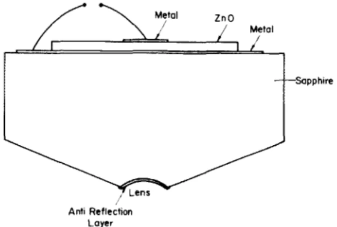
The heart ofthe acoustic microscope system is its acous-tic objective (Fig. 4). It converts the electrical signals fed to it into ultrasonic signals, focuses them to a diffraction-limit-ed spot, and converts the reflectdiffraction-limit-ed acoustic signals back to electrical form. The lenses are manufactured from single-crystal sapphire which is suitably oriented. Sapphire is se-lected for its high acoustic velocity to help reduce the spheri-cal aberrations and also for its hardness to make a durable and robust lens. A spherical lens cavity is ground on one side of the sapphire with mechanical means. Extreme care is ex-ercised to assure the sphericity of the cavity, because it is very crucial to reach the theoretical resolution limit. A ZnO thin-film transducer is deposited on the flat side of the crys-tal using an rf sputtering station. ZnO has a high piezoelec-tric coupling constant and is compatible with sapphire sub-strate. The size of the circular transducer is adjusted for minimum diffraction loss. The transducer generates planar acoustic wave fronts when used as transmitter, and as a re-ceiver it is sensitive to the shape of the wave fronts impinging on it. Therefore, it is not just an intensity detector as is the case for an optical detector. The lens cavity is coated with a
Electncal Input
Anti Reflection Layer
FIG. 4. Cross-sectional view of the acoustic objective.
Metal
I
Sapphire
quarter-wavelength-thick glass antireflection layer to re-duce the reflection loss as the waves travel from high-imped-ance sapphire to low-impedhigh-imped-ance liquid-coupling medium and vice versa. The two-way conversion loss of transducers is typically 10 dB, and the transmission loss through the coated lens element is less than 3 dB. The lens units are housed in small metallic tubes with the high-frequency con-nector on one end and the lens on the other. Matching net-works made from microstrip and/or discrete components are also included within the lens housing.
Because of bandwidth limitations, the whole frequency range cannot be taken care of with a single acoustic objec-tive. Instead, the 0.S-2.0-GHz range is divided between two objectives: one centered at 1 GHz and the other at 1.7 GHz. The lower-frequency 50-S00-MHz range is covered by ob-jectives operating at the following center frequencies: 50,
100,200, and 400 MHz. All the objectives have the associat-ed matching networks to give 15%-20% bandwidth. The higher-frequency objectives typically have much higher bandwidth, because the frequecy-dependent loss in liquid medium tends to compensate the mismatch loss. For exam-ple, it is possible to cover the entire frequency range 1.3-2 GHz with a single acoustic objective.
The acoustic objectives differ not only in frequency but also in radius of lens cavity. At high frequencies the loss in the liquid medium is very high. In this case the lenses with a cavity radius of 50 flm are used. On the other hand, at low frequencies the liquid losses drop very rapidly, making large radius lenses possible. At the low-frequency end 2000-flm
radius lenses are used to increase the working distance and to make higher penetration distances possible. For purposes of comparison, a 50-flm lens at 2 GHz causes a water l.oss of92 dB at 25 OC (55 dB at 60 ·C), whereas a 2000 flm lens at 100 MHz causes a water loss of only 9.2 dB.
Working with large radius lenses is easy both from me-chanical and from electrical points of view. Meme-chanically, there is a big play room, and electrically, the various internal reflection pulses are well separated from each other. It is quite easy to pick up the useful pulse and kill the others. For small radius lenses the task is quite difficult, however. For a
50-flm radius lens there is only 60-ns separation between the first internal reflection pulse and the object pulse. Addition-ally, the size of the object pul.se is 60 dB below the spurious
2572 Rev. Sci.lnstrum., Vol. 57, No. 10, October 1986
pulse. In this case one needs extremely short pulses with high reflection-loss electronics. Any reflection in electronics or in cables will manifest itself as interference of object pulse with a reference. This will result in annoying interference lines on the images. The high-frequency electronics described above are capable of separating the small object pulse from its large and close neighboring spurious pulses to generate interfer-ence-free images.
The objectives of varying lens radius have varying time delays. The object pulse will not appear at the same place for the different objectives. Hence the delays of time-gating pulses as generated by the pulse-drive circuitry shouJ.d be different. User adjustment of these delays would have been not only time consuming and boring, but also very difficult. This time delay adjustment is made automatically for every acoustic objective by the microprocessors.
In complete analogy with the opticallenses,f number of acoustic lenses is determined by the opening angle and the focallength.20 A smaner f-number (larger opening angle) lens would result in a higher resolution, but the penetration ability of such a lens would be lower. The
f
number of the lens must be properly selected to maximize the penetration ability with the given object material.The surface of the acoustic lens may get contaminated during operation or otherwise. A partial blocking of the lens will reduce the signal level but will not cause a noticeable resolution loss. Removal of the dirt from the lens surface is achieved by a motor-driven water jet at the side of the scan-ning table. When the optical microscope is in operating
posi-t~on, the water jet aligns with the lens axis, and an applica-hon of water cleans the lens surface acceptably. In stubborn cases it may be necessary to use a cotton-tipped applicator to remove the dirt.
Figure 5 shows an acoustic objective used by ELSAM. It is suitable in the frequency range 1.3-2.0 GHz. The lens is formed by a spherical cavity of 4O-,um radius at the tip of a sapphire single crystal. This crystal is attached to the front end of the metal objective housing. The piezoelectric trans-ducer is on the flat back side of the sapphire element inside the housing, and it is fabricated by rf-sputtering ZnO. The housing also contains a micros trip impedance matching network. In order to keep the moving mass of the scanner small, special attention has been paid to miniaturization of the objective. The frequency of operation can be changed by replacing the acoustic objective screwed on the scanner with an objective of the required frequency, followed by suitable commands on the user terminal.
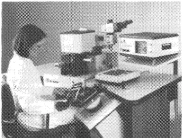
Figure 6 depicts the ELSAM in its acoustic imaging mode. Referring to the figure, the housing dose to the center contains the scanning mechanism for x-y movement of the acoustic objective. The acoustic objective is located under the housing and cannot be seen in this picture. The rotatable and tihable stage with micrometer spindles for x andy posi-tioning of the specimen is visible below the scanner housing. The light microscope, here out of its operating position, is on the right-hand side of the scanner housing. The light micro-scope and the acoustic micromicro-scope are mounted on a preci-sion rotating table for exact and rapid switching between the two modes. At the rear right is a long-persistence CRT
FIG. 5. Acoustic objective for the frequency range 1.3-2.0 GHz.
screen for real-time display of the acoustic slow scan image.
On the table below is the user terminal with joystick and function display. A photomicrographic unit with a high-re-solution CRT screen is located in front of the user terminal. The high-frequency electronics cabinet is at the back of the rotating table. The video, scan, and control electronics ca-binet and the frame store unit with video monitor are not shown in the figure.
FIG. 6. ELSAM in acoustic imaging mode.
2573 Rev. Sci.lnstrum., Vol. 57, No. 10, October 1986
(01 (c 1
(dl
FIG. 7. Acoustic images ofa resolution test grating with a period of 0.8 J..Im taken at different frequencies: (a) 1.4 GHz, (b) 1.6 GHz, (c) 1.8 GHz, and
(d) 2.0GHz.
II. JMAGES AND DISCUSSION
In this section we will present some images to demon-strate the ability of an acoustic microscope.
An
images are obtained from ELSAM high-resolution CRT screen with a 35-mm camera attached to it. Brighter pixels represent high-er levels of received signal from the corresponding object point. Darker pixels do not necessarily indicate that the acoustic energy at the object is absorbed; the reduction of the signal may be a result of a cancellation at the phase-sensitive transducer.Figure 7 shows the acoustic images of a resolution test grating taken at different operating frequencies 1.4-2.0 GHz. The period of the grating is 0.8 flm. The grating is unresolved in (a) but resolved in (b), (c), and (d). The theoretical resolution at the surface of the object is deter-mined by the sound wavelength in the immersion medium, the frequency of operation, and the! number of the lens. The sound velocity in water is 1500 m/s. The calculated resolu-tion value at 1.6 GHz is 0.8 flm. Figure 7 (b) clearly demon-strates that ELSAM is reaching this value.
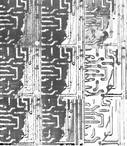
Figure 8 displays the acoustic images of a defective inte-grated circuit, taken at a wide range of frequencies. The de-fect is an overcharge-induced crack and delamination. This series clearly depicts the loss of lateral and z resolution towards lower frequencies. The high penetration, on the oth-er hand, is possible only at low opoth-erating frequencies. We note that for acoustically high-impedance (heavy and stiff) materials the penetration depth is limited by the wavelength of Rayleigh waves on the object surface. Because the longitu-dinal or shear acoustic waves cannot penetrate the object because of a high-impedance mismatch between the liquid immersion medium and the object, but Rayleigh waves can be excited with good efficiency regardless of the impedance of the object. The excited Rayleigh waves will leak back to the liquid medium, carrying the object-related subsurface information to the acoustic objective.21 On the other hand,
for low-impedance (light and soft) materials, both longitu-dinal and shear acoustic waves can penetrate into the object with a resonable focusing performance. In this case, the
etration depth is limited by the focal length of the acoustic objective and the sound attenuation in the material. High penetration depth in high-impedance materials can be achieved if a high-impedance immersion liquid such as mer-cury22 or gallium"3 is used. However, these liquids are diffi-cult to work with, and they are not compatible with most objects.
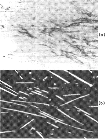
We present a comparison between optical and acoustic microscopic images in Fig. 9 to demonstrate the subsurface imaging abilities of the acoustic microscope. The sample is a glass-fiber-reinforced polycarbonate. The fibers are about 15
f..lm below the surface. The glass fibers are not visible in the optical micrograph, because the matrix is not transparent for tight. On the other hand, the acoustic micrograph showing the same area displays the fiber distribution clearly. The acoustic focus iii about 15 f..lm below the surface.
Figure 10 depicts acoustic images of a silicon-integrated circuit taken at frequencies 100,200, and 400 MHz. There is a proportional increase in the resolution of the images. Note the existence of surface acoustic wave (SAW) reflections at the surface as artifacts.24 The second set of images at the
same frequencies are with a 2S0-pm-thick mica sheet
insert-2574 Rev. ScI. Instrum., Vol. 57, No. 10, October 1986
FIG. 8. Acoustic images of a defective inte-grated circuit, taken at a wide range of fre-quencies: 2.0. 1.8, 1.6, 1.4, 1.2, 1.0,0.8, 0.6, 0.4, and 0.2 GHz, from top to bottom and left to right. respectively. The picture width is 200/1-m.
ed between the acoustic lens and the object surface all im-mersed in water. Clearly, 250 J..lm is penetrated at 100 and 200 MHz. But at 400 MHz nothing was detected, possibly because of the excessive loss in the mica sheet. At 200 MHz there is actually an apparent increase in resolution due to disappearance of SAW reflections at the edges. We believe that this is due to anisotropic attenuation in the mica sheet which has a highly directive molecular structure. The acous-tic rays at angles away from the normal direction are the ones exciting the SAW on the surface, and they are attenuat-ed more than the rays around the normal., hence giving rise to a better image.
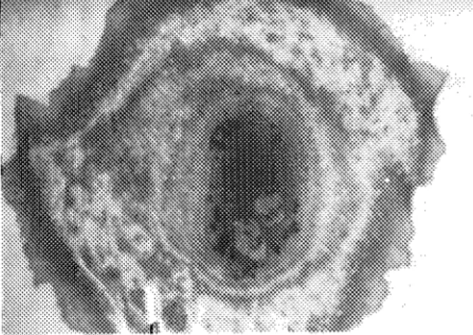
Biological cells are the most critical samples for acoustic microscopy,25 since the intensity modulation by the cell is very small compared to the "hard" materials. Moreover, the coupling medium cannot be heated up to improve the signal-to-noise ratio. Figure 11 shows the acoustic micrograph of a frog heart cell. The fringes outline the cel.l topography. The intensity of fringes can be related to the cell stitfness?6 The acoustic image also brings out the stress fibers and internal. details of the cell which are not visible in an optical. image. Live biological organisms can be observed by ELSAM with
(0 )
(b)
FIG. 9. (a) Optical and (b) acoustic images of glass-tiber-reinforced poly-carbonate. Acoustic image is taken at a ff(~quency of 1.0 GHz. Picture width is400f.lm.
(a) (b)
minimal disturbance to organisms at a water temperature of 35°C. They result in a reasonable level of contrast without need of staining. The scan rate is fast enough to freeze their motions if they are moving.
m.
CONCLUSIONSA new tool has been added to the avail of the scientists to investigate the microscopic world after the development of the commercial acoustic microscope. Basically, it is a micro-scope capable of subsurface imaging with a resolution equal-ing a good optical microscope. Optically opaque materials or layers, which are unsuitable for the optical microscope, be-come the objects of the acoustic microscope. The scanning electron microscope can reach an extremely high resolution with a very high depth offield, but it operates under vacuum and is suitable only for a class of objects. Some objects will need a metallization step before imaging. The acoustic mi-croscope can be used nondestructively with almost all ob-jects. It is sensitive to a change in density or stiffness of the material. Voids within the body of the materials or delamin-ations in thin-film structures are easily detected because of very high acoustic-impedance change at the interface.
The acoustic microscope is designed with microcom-puters controlling its functions and its operation. The use of microcomputers makes the realization of a complicated in-strument with many functions possible as a reliable and user-friendly machine. It allows use of relatively low-cost high-frequency components with their deficiencies compensated
(c)
FIG. 10. Acoustic images of a silicon-integrated circuit. taken at frequencies (a) 100 MHz. (b) 200 MHz. and (c) 400 MHz. The bottom row images are taken with a 250-f.lm mica sheet placed on the object surface. The width of the images are about 800 /l-m.
FIG. 11. Acoustic micrograph ofa frog heart cell at a frequency of 1.6 GHz. The picture width is 200 ""m.
in the software. It allows easy service and maintenance as well as expansion possibilities for future upgrades and im-provements.
The commercial development of a versatile acoustic mi-croscope has led to accelerated application research. After the availability of the instrument, many advantages of the acoustic microscope have been discovered over an optical microscope or a scanning electron microscope. But the acoustic microscope should not be seen as a competitor of those microscopes. On the contrary, it complements them when used in conjunction with them. The scanning acoustic microscope has found applications in such diverse fields as materials science, thin-film technology, geology, and biol-ogy, and new fields are emerging as the application research continues.
2576 Rev. Sci.lnstrum., Vol. 57, No. 10, October 1986
ACKNOWLEDGMENTS
The authors would like to thank all members of the acoustic microscope development team, and especially A. Thaer, D. Huelsman, H. Muth, and H. Fischbach.
IIEEE Trans. Sonics Ultrasonics, Special Issue on Acoustic Microscopy (1985).
'Scanned Image Microscopy, edited by E. A. Ash (Academic, London, 1980).
3R. G. Wilson and R. D. Weglein, 1. App!. Phys. 55, 3261 (1984). 4J. K. Wang and e. S. Tsai, J. App!. Phys. 55, 80 (1984). 'R. Hammer and R. L. Hollis, App!. Phys. Lett. 40, 678 (1982).
"Y. lipson and e. F. Quate, App!. Phys. Lett. 32, 789 (1978).
71. Kushibiki, A. Ohkubo, and N. Chubachi, Electron. Lett. 18, 663 ( 1982).
"y. Guangqi, M. Nikoonahad, and E. A. Ash, Electron. Lett. 18, 767 (1982).
9B. Nongaillard, J. M. Rouvaen, E. Bridoux, R. Torguet, and C. Brunee1, 1. App!. Phys. 50,1245 (1979).
10M. Poirier, M. Castonguay, e. Neron, and J. D. N. Cheeke, J. App!. Phys. 55,89 (1984).
II A. I. Morozov and M. A. Kulakov, Electron. Lett. 16, 596 (1980). 12R. Lemons and e. F Quate, App!. Phys. Lett. 24, 163 (1974). J3e. F. Quate, A. Atalar, and H. K. Wickramasinghe, Proc. IEEE 67. 1092
(1979).
14M. Hoppe, A. Atalar, W. J. Patze!t, and A. Thaer. Leitz-Mitt. Wiss. u. Techn. VIII, 125 (1983).
15M. Hoppe and 1. Bereiter-Hahn, IEEE Trans. Son. Ultrason. 5U-32, 289 (1985).
10H. K. Wickramasinghe. J. Microsc. (Oxford) 129,63 (1983). I7B. Hadimioglu and e. F. Quate, App!. Phys. Lett. 43. 1006 (1983). 18J. Heiserman, D. Rugar, and e. F. Quate, J. Acoust. Soc. Am. 67, 1629
(1980).
19e. R. Petts and K. Wickramashinghe, Electron. Lett. 16.9 (1980). '''A. Atalar. IEEE Trans. Son. Vltrason. 5U-32. 164 (1985).
"w.
Parmon and H. L. Bertoni, Electron. Lett. 15, 684 ( 1979). "1. Attal. in Scanned Image Microscopy, edited by E. A. Ash (Academic,London, 1980)' p. 97.
"Y. lipson. App!. Phys. Lett. 35, 385 (1979).
14K. Yamanaka and Y. Enomoto, Electron. Lett. 17,638 (1981). "R. N. 10hnston. A. Atalar, J. Heiserman, V. Jipson, and e. F. Quate. Proc.
Nat!. Acad. Sci. U.S.A. 76. 3325 (1979).
'61. Hildebrand and D. Rugar, 1. Microsc. (Oxford) 134.245 (1984).
AcousUc microscope 2576
View publication stats View publication stats