Europhys. Lett., 56 (1), pp. 41–46 (2001)
Photonic band gaps and localization in two-dimensional
metallic quasicrystals
M. Bayindir, E. Cubukcu, I. Buluand E. Ozbay
Department of Physics, Bilkent University - Bilkent, 06533 Ankara, Turkey (received 5 January 2001; accepted in final form 12 July 2001)
PACS.42.70.Qs – Photonic bandgap materials. PACS.61.44.Br – Quasicrystals.
PACS.71.15.Ap – Basis sets (plane-wave, APS, LCAO, etc.) and related methodology (scat-tering methods, ASA, linearized methods).
Abstract. – We report on experimental observation of photonic stop bands in two-dimensional
metallic Penrose lattice. We investigated the defect characteristics, and observed strongly lo-calized cavity modes below the plasma frequency. The absence of the translational symmetry allowed to change the defect frequencies and localization properties of the defect modes. Propa-gation of photons along highly localized coupled-cavity modes was experimentally demonstrated in quasiperiodic metallic structures.
The artificially created periodic structures, photonic band gap (PBG) materials, inhibit the propagation of electromagnetic (EM) waves in certain frequency ranges in analogy with electronic band gaps in semiconductors [1, 2]. In semiconductors, only short-ranged order is necessary for the formation of electronic band gaps [3]. Therefore, the existence of stop bands for photons in quasiperiodic or random structures has a fundamental importance. Recently, it was shown that the propagation of EM waves through two-dimensional (2D) quasiperiodic dielectric photonic crystals is forbidden for certain wavelengths [4–10]. Even if the quasiperi-odic structures are characterized by a lack of long-range periquasiperi-odic translational order, these systems have long-range bond-orientational order. Therefore, a quasiperiodic system can be considered as an intermediate between periodic and completely random systems [11, 12].
Photonic crystals have inspired great interest because of their scientific and technological applications. However, most of the attention has been concentrated on dielectric-based struc-tures. Although metals exhibit high absorption at optical frequencies, some specific properties of metals can be used at microwave and millimeter-wave applications [13–18]. In this letter, we experimentally show that a 2D Penrose lattice exhibits photonic stop bands for certain frequency ranges and strong photon localization in the vicinity of the plasma frequency. More-over, we investigate the guiding of EM waves through a coupled-cavity array which was formed by removing rods from the Penrose lattice.
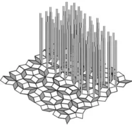
The Penrose tiles [19, 20] are composed of fat and skinny rhombic unit cells, and fill the 2D plane nonperiodically as illustrated in fig. 1. The Penrose tiling is self-similar and has many interesting properties such as macroscopic tenfold symmetry, long-range decagonal
c
Fig. 1 – Schematic drawing of a two-dimensional Penrose photonic crystal. The metallic rods are placed at all vertices of fat and skinny rhombic cells.
bond-orientational symmetry, and many centers of local fivefold symmetry. The localization phenomena and spectral gaps were widely studied in the 2D Penrose lattice of electronical [21, 22] and acoustical [23, 24] systems. Recently, Krauss et al. demonstrated the diffraction pattern from a grating based on Penrose tiles [25].
We constructed a 2D Penrose lattice by placing cylindrical copper rods of radius r = 1.5 mm and length L = 15 cm at each vertices of the skinny and fat rhombic cells (see fig. 1). The side of each rhombus was a = 1.2 cm. The experimental set-up consisted of a HP 8510C network analyzer and microwave horn antennas to measure the transmission amplitude and transmission-phase spectra. We measured only transfer magnetic (TM) fields in which the incident electric field, E, was parallel to the rods. It is a well-known fact that the other polarization, transfer electric (TE), does not produce any photonic band gaps in this frequency range [1].
We first measured transmission through a perfect metallic Penrose lattice by varying the incidence angle. The crystal consisted of 236 rods, and had a rectangular shape having dimensions 13 cm× 13 cm corresponding to a filling fraction η ∼ 0.1 (right panel in fig. 2). As shown in left panel of fig. 2, we observed a narrow forbidden gap centered at frequency 20.30 GHz, which originated from the periodicity of the structure just as in periodic photonic crystals [13, 17]. We also observed that all EM waves were excluded from the crystal within a frequency range extending from zero frequency to the plasma frequencyωp= 15.03 GHz for θ = 0◦. This metallicity gap was already observed in periodic [13–17] and disordered [26, 27] metallic photonic crystals. As we increased the incidence angle, we observed that the plasma frequency shifted to the higher frequencies, and the width of the photonic band gap increased. It is important to note that we performed the measurements up to 40 GHz, and we did not observe any other gaps in the transmission spectrum.
Next, we investigated defect characteristics of metallic Penrose lattice for two different cases: 1) we removed various numbers of rods to achieve defects with different cavity volumes and 2) we removed two neighboring rods to achieve defects with a fixed cavity volume. For both cases, the crystal consisted of 98 metallic rods having a rectangular shape. In the former case, we removed two, three, and four neighboring rods as indicated in the right panel of fig. 3, respectively. As shown in fig. 3 (left panel), we observed strongly localized defect modes within
θ 12 14 16 18 20 22 Frequency (GHz) -60 -50 -40 -30 -20 -10 T ransmission (dB) θ=0o θ=9o θ=18o θ=27o θ=36o Plasma ( Frequency Photonic Band Gap Transmitter Receiver
Fig. 2 – Left panel: measured transmission spectra for various incidence angles. The crystal exhibits a plasma frequency around 15.03 GHz and a photonic band gap centered around 20.30 GHz. Right panel: schematics of the experimental set-up. The (•) symbols denote vertices of the Penrose lattice.
the metallicity gap close to the plasma frequency. The corresponding defect frequencies were fA = 14.00 GHz, fB = 13.59 GHz, and fC = 12.73 GHz. The quality factors, defined as
center frequency divided by the peak’s full width at half-maximum, of these cavities were measured to be QA = 795, QB = 660, and QC = 861. Higher cavity volume resulted in a shift of the defect mode to the lower frequencies (longer wavelengths) as expected. Indeed, the corresponding cavity modes also appeared in the photonic band gap with very low-quality factors. In the latter case, we removed two rods for each cavity by changing the location of one of these rods (see right panel in fig. 4). The measured transmission characteristics were plotted in the left panel of fig. 4. It was observed that the defect frequency can be changed by varying the position of missing rods even if all cavities had the same cavity volume.
12 14 16 18 20 22 Frequency (GHz) -60 -50 -40 -30 -20 -10 0 T ransmission (dB) A B C A B C A B C
Fig. 3 – Left panel: measured transmission spectra of three defects having different cavity volume which were constructed by removing rods from a Penrose crystal consisting of 98 metallic rods. Highly localized defect modes were observed below the plasma frequency. Right panel: the (•) and (◦) symbols denote vertices of the Penrose lattice and removed rods, respectively.
12 14 16 18 20 22 Frequency (GHz) -50 -40 -30 -20 -10 0 T ransmission (dB) A B C A B C A B C
Fig. 4 – Left panel: measured transmission spectra of the cavities which were constructed by removing two rods from a Penrose crystal consisting of 98 metallic rods. Highly localized defect modes were observed within the metallicity gap. Right panel: the (•) and (◦) symbols denote vertices of the Penrose lattice and removed rods, respectively.
The defect characteristics of a quasicrystal can be more interesting than ordinary periodic crystals due to the absence of long-range translational symmetry [4]. Therefore, we observed completely different localization properties and different defect frequencies by removing rods from various locations. This type of behavior cannot be achieved in a periodic photonic crystal. Recently, we have demonstrated a new type of propagation mechanism through an array of coupled cavities in one-dimensional structures [28], and three-dimensional layer-by-layer photonic crystals [29, 30]. In the coupled-cavity structures where the tight-binding approx-imation [31] is valid, photons hop from one evanescent defect mode to the neighboring one
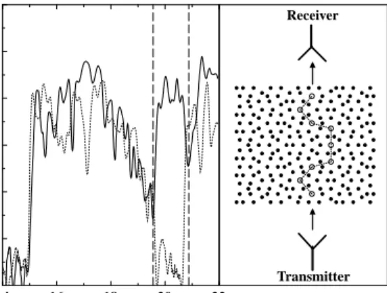
14 16 18 20 22 Frequency (GHz) -50 -40 -30 -20 -10 0 T ransmission (dB) Transmitter Receiver
Fig. 5 – Left panel: measured transmission through a coupled-cavity array which was constructed by removing neighboring rods (solid line). Transmission characteristics of a perfect Penrose lattice are plotted as a comparison (dotted line). Right panel: the (◦) symbols represent the removed rods and the dotted line indicates the propagation direction of the EM wave along the strongly localized coupled-cavity modes.
due to the overlapping between the tightly confined modes at each defect site. Due to the coupling between the localized cavity modes, a photonic defect band (waveguiding band) is formed within the photonic band of the crystal analogous to the transition from atomic-like discrete states to the continuous spectrum in solid-state physics.
In order to demonstrate the guiding of EM waves through a coupled-cavity waveguide (CCW) in the present structure, we removed 9 neighboring rods which have similar surround-ing environments as indicated in fig. 5 (right panel). The measured transmission spectrum cor-responding to this coupled-cavity array is shown in the left panel of fig. 5 (solid line). We also plotted the transmission spectrum of the perfect Penrose lattice as a comparison (dotted line). We observed a defect (waveguiding) band in photonic band gap extending from 19.54 to 20.88 GHz. Since each defect leads to two distinct cavity modes in the metallicity gap and in the photonic band gap, it is expected that two defect bands were formed due to the coupling between the localized cavity modes. However, as shown in fig. 5 (left panel) we achieved the waveguiding phenomena only in photonic band gap. Measurements did not exhibit any other defect band below the plasma frequency. This result may be due to the quasiperiodic nature of the crystal, and is in contrast to what we observed in metallic periodic photonic crystals where we achieved the corresponding waveguiding bands in both metallicity and photonic band gaps [27].
Since the quasicrystal structures are situated between periodic crystals and completely disordered systems, it is natural to ask the following question. What would happen in a com-pletely disordered metallic lattice? Recently, it was observed that the photonic band gap that originated from the periodicity quickly disappeared in the presence of disorder [26, 27]. How-ever, the metallicity gap persisted even if a large amount of disorder was introduced. Wave-guiding along the coupled-cavity structures was also achieved in weakly disordered metallic photonic crystals [27].
In conclusion, we experimentally observed that Penrose-type quasiperiodicity produced a stop band for EM waves for a certain frequency range just as in periodic metallic and dielectric photonic crystals. A metallicity gap appeared, starting from zero frequency to the plasma frequency. By removing rods from the perfect crystals, we obtained highly localized defect modes just below the plasma frequency. The defect frequency could be changed either by removing more rods (larger defect volume) or changing the position of defect site. We also achieved the guiding of EM waves along a specific coupled-cavity path on the Penrose lattice.
∗ ∗ ∗
This work was supported by NATO Grant No. SfP971970, National Science Foundation Grant No. INT-9820646, Turkish Department of Defense Grant No. KOBRA-001, and Thales JP8.04.
REFERENCES
[1] Joannopoulos J. D., Meade R. D. and Winn J. N., Photonic Crystals: Molding the Flow
of Light (Princeton University Press, Princeton, NJ) 1995.
[2] Soukoulis C. M. (Editor), Photonic Band Gap Materials (Kluwer, Dordrecht) 1996. [3] Yu P. Y. and Cardona M., Fundamentals of Semiconductors: Physics and Materials
Prop-erties (Springer-Verlag, Berlin, Heidelberg) 1996.
[4] Chan Y. S., Chan C. T. and Liu Z. Y., Phys. Rev. Lett.,80 (1998) 956.
[5] Jin C., Cheng B., Man B., Li Z. and Zhang D., Appl. Phys. Lett.,75 (1999) 1848. [6] Cheng S. S. M., Lie-Ming Li, Chan C. T. and Zhang Z. Q., Phys. Rev. B,59 (1999) 4091.
[7] Jin C., Cheng B., Man B., Li Z. and Zhang D., Phys. Rev. B,61 (2000) 10762.
[8] Zoorob M. E., Charlton M. D. B., Parker G. J., Baumberg J. J. and Netti M. C.,
Nature (London),404 (2000) 740.
[9] Zhang X., Zhao-Quing Zhang and Chan C. T., Phys. Rev. B,63 (2001) 081105(R). [10] Bayindir M., Cubukcu E., I, Bulu and Ozbay E., Phys. Rev. B,63 (2001) 161104(R). [11] Levine D. and Steinhardt P. J., Phys. Rev. B,34 (1986) 596.
[12] Steinhardt P. J. and Ostlund S., The Physics of Quasicrystals (World Scientific, Singapore) 1987.
[13] Sievenpiper D. F., Sickmiller M. E. and Yablonovitch E., Phys. Rev. Lett., 76 (1996) 2480.
[14] Pendry J. B., Holden A. J., Stewart W. J. and Youngs I., Phys. Rev. Lett.,76 (1996) 4773.
[15] Ozbay E., Temelkuran B., Sigalas M. M., Tuttle G., Soukoulis C. M. and Ho K. M.,
Appl. Phys. Lett.,69 (1996) 3797.
[16] Temelkuran B., Altug H. and Ozbay E., IEE Proc. Optoelectron.,145 (1998) 409. [17] Pendry J. B., Holden A. J., Robbins D. J. and Stewart W. J., IEEE Trans. Microwave
Theory Tech.,47 (1999) 2075; J. Phys. Condens. Matter, 10 (1998) 4785.
[18] Sievenpiper D. F., Yablonovitch E., Winn J. N., Fan S., Villeneuve P. R. and Joannopoulos J. D., Phys. Rev. Lett.,80 (1998) 2829.
[19] Penrose R., Bull. Inst. Math. Appl.,10 (1974) 266. [20] Gardner M., Sci. Am.,236 (1977) 110.
[21] Kohmoto M. and Sutherland B., Phys. Rev. Lett.,56 (1986) 2740. [22] Vidal J., Mosseri R. and Doucot B., Phys. Rev. Lett.,81 (1998) 5888. [23] He S. and Maynard J. D., Phys. Rev. Lett.,62 (1989) 1888.
[24] de Espinosa F. M. and Torres M., Appl. Phys. Lett.,65 (1994) 1352. [25] Krauss T. F. and De La Rue R. M., Prog. Quantum Electron.,23 (1999) 51. [26] Guida G., Opt. Comm.,156 (1998) 294.
[27] Bayindir M., Cubukcu E., Bulu I., Tut T., Ozbay E. and Soukoulis C. M., unpublished. [28] Bayindir M., Tanriseven S. and Ozbay E., Appl. Phys. A,72 (2001) 117.
[29] Bayindir M., Temelkuran B. and Ozbay E., Phys. Rev. Lett.,84 (2000) 2140 and references therein.
[30] Bayindir M., Temelkuran B. and Ozbay E., Phys. Rev. B,61 (2000) R11855.
[31] Ashcroft N. W. and Mermin N. D., Solid State Physics (Sounders, Philadelphia) 1976, p. 175.