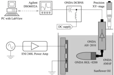
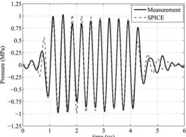
0885–3010/$25.00
©
2012 IEEEHigh-Power CMUTs: Design
and Experimental Verification
F. yalçin yamaner, Member, IEEE, selim olçum, Member, IEEE,
H. Ka
ğan oğuz, Student Member, IEEE, ayhan Bozkurt, Member, IEEE,
Hayrettin Köymen, Senior Member, IEEE, and abdullah atalar, Fellow, IEEE
Abstract—Capacitive micromachined ultrasonic transducers (CMUTs) have great potential to compete with piezoelectric transducers in high-power applications. As the output pres-sures increase, nonlinearity of CMUT must be reconsidered and optimization is required to reduce harmonic distortions. In this paper, we describe a design approach in which uncol-lapsed CMUT array elements are sized so as to operate at the maximum radiation impedance and have gap heights such that the generated electrostatic force can sustain a plate displace-ment with full swing at the given drive amplitude. The pro-posed design enables high output pressures and low harmonic distortions at the output. An equivalent circuit model of the array is used that accurately simulates the uncollapsed mode of operation. The model facilities the design of CMUT pa-rameters for high-pressure output, without the intensive need for computationally involved FEM tools. The optimized design requires a relatively thick plate compared with a conventional CMUT plate. Thus, we used a silicon wafer as the CMUT plate. The fabrication process involves an anodic bonding pro-cess for bonding the silicon plate with the glass substrate. To eliminate the bias voltage, which may cause charging prob-lems, the CMUT array is driven with large continuous wave signals at half of the resonant frequency. The fabricated arrays are tested in an oil tank by applying a 125-V peak 5-cycle burst sinusoidal signal at 1.44 MHz. The applied voltage is in-creased until the plate is about to touch the bottom electrode to get the maximum peak displacement. The observed pres-sure is about 1.8 MPa with −28 dBc second harmonic at the surface of the array.
I. Introduction
c
apacitive micromachined ultrasonic transducers
(cMUTs) are used to generate and detect ultrasound
[1], by utilizing a microfabricated suspended moving plate
for the transduction. recent improvements in cMUT
de-signs [2]–[4] and operating methods [5], [6] and advances
in the fabrication methodology [7]–[9] demonstrate
prom-ising results which make the cMUT technology a strong
candidate for different ultrasound applications [10]–[15].
High-intensity focused ultrasound (HIFU) is a
high-power applications in which sound waves are focused on
abnormal tissue and destroy it by delivering high energy
[16]. recently, it has been demonstrated that cMUTs can
be used as HIFU transducers [17], [18]. cMUTs can be
fabricated using silicon as a membrane material which has
high thermal conductivity and can eliminate the
require-ment of a cooling system [19]. The monolithic
integra-tion of imaging and HIFU cMUTs has been realized and
tested [20]. Magnetic resonance (Mr) compatible cMUTs
with different plate topologies have been fabricated, and
it has been shown that the output pressures can be
in-creased by using piston-shaped plates [21]. cMUTs with
dual electrodes enable leveraged bending and increase the
total displacement of the plate in the transmit operation
[3], [22]. Using side electrodes, it is possible to move the
plate in a wider displacement range without collapsing;
however, the voltages required for bending the plate are
higher when compared with a cMUT with full electrode
coverage.
In this paper, we propose a methodology to design and
operate cMUTs to generate single tone, high-amplitude
pressure waves with low harmonic content. We employ an
equivalent circuit that was developed in [23]. We excite
the cMUT at half of the resonance frequency of the plate
without a dc bias voltage to reduce the harmonic content
and the effect of the charge trapping within the thin
di-electric layer between the cMUT electrodes.
II. nonlinear Equivalent circuit Model
The electrode coverage of a cMUT plays a major role
in both transmit and receive operations. Usually, cMUTs
are designed with half electrode coverage for the receive
mode to optimize the receive sensitivity [24]. However a
higher transmit sensitivity is possible with full electrode
coverage, because a larger electrode increases the total
electrical force acting on the plate. Therefore, we choose
to utilize a cMUT structure with full electrode coverage
to generate the maximum pressure for a given voltage.
Fig. 1 shows a representative cross section of a circular
cMUT cell.
although a suspended circular plate is modeled by a
linear spring, cMUT operation is not linear because of the
nonlinear dependence of the electrical force on the plate
position. In this work, we use the nonlinear equivalent
circuit model shown in Fig. 2 [23], [25].
Manuscript received october 18, 2011; accepted March 26, 2012. This work was supported by the scientific and Technological research coun-cil of Turkey (TUBITaK) under project grant 107T921 and 110E216.
F. y. yamaner and a. Bozkurt are with the Electronics Engineer-ing department, sabanci University, Istanbul, Turkey (e-mail: yalcin@ sabanciuniv.edu).
s. olçum was with and H. K. oğuz, H. Köymen, and a. atalar are with the Electrical and Electronics Engineering department, Bilkent University, ankara, Turkey.
s. olçum is now with the department of Biological Engineering, Mas-sachusetts Institute of Technology, cambridge, Ma.
A. Circuit Model Components
In the electrical part of the equivalent circuit, C
0is
the shunt input capacitance of the cMUT, i
cis the
non-linear component of the capacitive current, and i
velis the
motion-induced current that accounts for the movement
of the plate. The mechanical part of the circuit is on the
right-hand side. The electrical attraction force, f
r, and the
force exerted by the atmospheric pressure, F
bare
repre-sented by voltage sources. The mass and the compliance
of the plate are represented by an inductor, L
rm, and a
ca-pacitance, C
rm, respectively. The expressions for
calculat-ing the circuit parameters can be found in the appendix.
The radiation impedance of the medium is modeled by
an impedance, Z
rr, terminating the acoustic port of the
circuit. The parameter N represents the number of cells
in an array and provides scaling to the equivalent circuit.
The behavioral current and voltage sources in the circuit
require the instantaneous peak displacement of the plate,
x
P, as a parameter; x
Pis calculated by a small subcircuit
depicted separately at the bottom of Fig. 2. The
subcir-cuit calculates the displacement by dividing the restoring
force of the plate, F
rm, by the plate compliance.
B. Thick Plates
The expressions for calculating the force and
compli-ance relations assume a thin plate approximation [23],
[25]. Using this approximation, the first series resonance
frequency of the plate can be calculated precisely for t
m/a
< 0.1 [9]. If the plate is not thin, the accuracy of the
model degrades. Using finite element modeling (FEM)
simulation results for thick plates, a correction factor is
applied to C
rm:
C
RmC
Rmt
a
mt a
mfor /
′
=
1.019
+
5.005
1.981
< 0
..8.
(1)
With this modification, the resonance frequency
deter-mined from the circuit model is in good agreement with
FEM simulation results. The model loses its accuracy for
frequencies close to the antiresonance frequency, because
a first-order LC circuit is inadequate to model high-order
modes of a cMUT plate [26]. Table I lists the material
properties used in the simulations.
In Fig. 3, we test the accuracy of the model in static
conditions for thick plates by comparing static deflections
obtained from FEM and sPIcE simulations for different
bias voltages.
Fig. 1. representative cross section of a circular plate with radius a, thickness tm, and gap height of tg. The top electrode is the high-con-ductivity silicon wafer. ti is the thickness of the insulation layer beneath the silicon wafer. The bottom electrode is a gold layer embedded in the substrate.
Fig. 2. Electrical circuit model of a capacitive micromachined ultrasonic transducer (cMUT) array driven by voltage source V(t). The radiation impedance, Zr, is modeled by an RLC circuit. N represents the number
of cells in the array.
Permittivity of sio2, ε i 3.9
density of water, ρ0 1000 kg/m3
speed of sound in water, c 1500 m/s
Fig. 3. comparison of the static deflections obtained from finite element modeling (FEM) and the sPIcE model for thick plates (a = 300 µm, tg
C. Radiation Impedance
The radiation impedances of a cMUT cell and an
ar-ray of cMUTs were calculated in [27] for conventional
mode of operation. The radiation impedance is a complex
quantity and a strong function of the ka product, where k
is the wavenumber. For an accurate simulation in sPIcE,
the radiation impedance can be modeled by using an RLC
network (Fig. 4) as in [28]. The component values are
defined in terms of the plate radius, a, the velocity of the
sound in the medium, c, the density of the immersion
medium, ρ
0, cell-to-cell separation, d, and the number of
cells in the array, N. The component values for
configura-tions with different numbers of cells, as shown in Fig. 5,
are given in Table II.
The accuracy of the network is demonstrated in Fig. 6
for N = 1 and N = 7. Using the parameters in Table II,
the network can be used to accurately model the radiation
impedance of an array with 19 cMUT cells, as well.
D. Circuit Simulations
The equivalent circuit in Fig. 2 is simulated with
lTspice (linear Technology, Milpitas, ca; http://www.
linear.com/designtools/software). Each circuit component
in the model is defined parametrically in terms of the
cMUT geometry and the material properties. The
per-formance of the equivalent circuit is tested by simulating
an excitation of a 2-cycle 95-V peak sinusoidal burst at
half of the resonance frequency of a cMUT cell. The
cen-ter displacement of the plate is compared with the FEM
simulation results in Fig. 7. The details of FEM model can
be found in [3].
The surface pressure can be calculated by dividing the
force across the radiation impedance by the surface area
of the cMUT cell. output power can be calculated by
taking average of the product of force and velocity over
the plate surface.
III. cMUT design
A. Excitation at Half of the Operating Frequency
conventionally, transmitting cMUTs are operated with
a bias voltage, which may degrade the device performance
Fig. 4. RLC model for the radiation impedance of a capacitivemicroma-chined ultrasonic transducer (cMUT) array.
Fig. 5. configuration of the capacitive micromachined ultrasonic trans-ducer (cMUT) array for different number of cells.
TaBlE II. component Values for the radiation Impedance Model With different numbers of cells in the array.
N 1 7 19 R1/Rn 0.64 0.39 0.48 L1/Rn 0.54 a/c 0.55 d/c 1.2 d/c C1Rn 0.2 a/c 1.38 d/c 1.22 d/c R2/Rn 0.90 0.02 1.4e-6 L2/Rn 0.37 a/c 0.77 d/c 2.3 d/c R3/Rn — 1.31 2.06 L3/Rn — 0.07 d/c 0.05 d/c C3Rn — 0.32 d/c 0.40 d/c R4/Rn — 1.04 1.12 L4/Rn — 0.28 d/c 0.29 d/c
Rn = π a2ρ0c/N; ρ0 = density of the plate material.
Fig. 6. comparison of the normalized radiation resistance and reac-tance of (top) a single capacitive micromachined ultrasonic transducer (cMUT) cell and (bottom) a cMUT array of 7 cells with the RLC model and actual values. (The normalization constant is πa2ρ0c/N, d = 2a.)
by causing charge trapping in the insulation layer [5], [29]
and drifting of the resonance frequency of the plate [30].
For continuous wave applications, it is possible to use
an excitation voltage, V(t), at half of the operating
fre-quency without a dc bias to excite cMUTs [31], [32]:
V t
( ) =
V
maxcos
ω
2
t
,
(2)
where V
maxis the peak voltage and ω is the operating
frequency. The force exerted on the plate, f
r, will be
pro-portional to
f
R( ) = 2 [1
V t
2V
max( )]
t
2
∝
+ cos
ω
.
(3)
as seen in (3), V
2(t) includes a dc term that will naturally
form a static force at the operating frequency.
B. Determination of CMUT Dimensions
We start by assuming that the peak drive voltage is
limited. The thickness of the insulation layer, t
i, is chosen
such that the insulation withstands the peak voltage
dur-ing the operation. For a maximum operatdur-ing voltage of
100 V, the insulation layer is chosen as silicon dioxide
1with a thickness of 200 nm.
let us assume that the target operating frequency is
3 MHz and we use an array configuration of 7 cells.
In-creasing the radiation resistance seen by the cMUT array
increases the power delivered to the medium [34].
There-fore, at the operating frequency we wish to maximize the
radiation resistance, which is maximum at ka = 3.75 for
an array of 7 cells, as seen in Fig. 6. Hence, the plate
radius maximizing the radiation resistance at 3 MHz is
298 µm. The cMUT plate must resonate at the desired
operating frequency to maximize the displacement. Using
the circuit model, t
mis found to be 130 µm.
To determine t
g, a 100-V peak continuous wave signal
at half of the resonance frequency (1.5 MHz) is applied
to the circuit model. t
gis reduced until the center of the
oscillating plate is about to touch the substrate. as seen
in Fig. 8, at t
g= 84 nm, the center peak displacement
of the plate reaches 80 nm. at this point, the resonance
frequency shifts because of the spring-softening effect [35].
To compensate for the spring softening, the thickness of
the plate is slightly increased and the last step is repeated.
after a few iterations, we find t
m= 135 µm and t
g=
80 nm.
For a target operating frequency and an available peak
voltage, the procedure for designing a high-power cMUT
is as follows:
1) choose the minimum insulation layer thickness, t
i,
maintaining a safe operation for a chosen maximum
drive voltage.
2) choose the plate radius, a, providing the maximum
radiation impedance at the operating frequency.
3) Find the plate thickness, t
m, required for a resonance
at the given operating frequency.
4) choose a large gap, t
g, and then reduce the gap step
by step until the plate is about to touch the
sub-strate in the positive force cycles.
5) If resonance frequency shifts, repeat the previous
two steps for a fine adjustment.
Table III lists the design parameters for continuous
3-MHz operation. as seen from the table, the cMUT
op-erating at the peak of the radiation impedance provides
the maximum pressure with a relatively low second
har-monic.
Fig. 7. a 2-cycle 95-V peak cosine burst at 1.3 MHz is applied to a ca-pacitive micromachined ultrasonic transducer (cMUT) cell under water loading. The effect of the atmospheric pressure (100 kPa) is taken into account (a = 300 µm, tm = 100 µm, tg = 100 nm, ti = 200 nm).
Fig. 8. The center displacement of the plate for different tg values under
a continuous 100-V peak 1.5-MHz sinusoidal signal (a = 298.5 µm, tm =
130 µm, ti = 100 nm).
1 The theoretical dielectric strength of silicon dioxide is ~1000 V/
The available input voltage changes the results
drasti-cally. When the available voltage is increased to 200 V
(t
i= 400 nm), the surface pressure reaches 3.5 MPa with
harmonics at −27 dBc for the optimum design.
The procedure is also applied to operating frequencies
of 1, 5, 10, and 15 MHz at 100 V maximum available
volt-age. cMUT dimensions for each design are given in Table
IV.
IV. Fabrication
For the fabrication of a high-power cMUT, we utilized
anodic wafer bonding technology. anodic bonding is used
to bond a silicon wafer to a borosilicate wafer using proper
pressure, electric field, and temperature. We defined the
cavity of the cMUTs on the silicon side. The
microfabri-cation process on the silicon side starts with a 76.2-mm
(3-in), highly doped, double-side-polished silicon wafer.
The microfabrication process is shown in Fig. 9. High
con-ductivity of this wafer serves as one of the electrodes of
the cMUTs. The thickness of the silicon wafer determines
the thickness of the cMUT plate, which is 92 µm in this
case. First, a 450-nm insulation layer of silicon oxide is
thermally grown in a diffusion furnace. The silicon wafer
is kept in the furnace at 1050°c for one hour in the
pres-ence of adequate water vapor. second, 100 nm of silicon
oxide is etched using a reactive ion etching (rIE) reactor
to create the cavities. as the final process on the silicon
side, the silicon oxide at the back side of the silicon wafer
is etched away using the rIE reactor.
Having completed the plate side, the substrate side is
fabricated on a 3.2-mm-thick 101.6-mm (4-in) borosilicate
wafer. The substrate wafer is chosen to be quite thick to
maintain a rigid substrate. Because the smoothness of the
borosilicate surface is critical for the success of the anodic
bonding, the substrate electrode is buried on the glass
wafer. an image reversal photoresist (aZ5214E,
clari-ant corp., Muttenz, switzerland) is used for the lift-off
process. Before the evaporation of the gold electrode, the
glass is etched approximately by the thickness of gold to
be evaporated. as the substrate electrode, 15 nm of
tita-nium and 85 nm of gold are deposited by thermal
evapo-ration. The borosilicate and silicon wafers are cleaned at
120°c in piranha etch (1:3 H
2o
2:H
2so
4) for 15 min
be-fore the bonding process. The prepared wafers are then
anodically bonded (applied Microengineering ltd.,
ox-fordshire, UK). The current passing during the bonding
process is limited to prevent dielectric breakdown, because
a bonding voltage up to 1000 V is utilized.
Because the borosilicate wafer is larger than the silicon
wafer, the substrate electrical contacts are made at the
TaBlE III. design comparisons at 3 MHz.a (µm) ka tm (µm) tg (nm) xp-p (nm) surface pressure (p-p, MPa) 2nd harmonic (dBc) Power/area (W/mm2) 20 0.25 1.18 280 331 1.42 −14.5 1.08 50 0.62 6.2 145 149 1.43 −6.7 1.14 100 1.25 16 144 186 1.66 −8.1 1.6 298 3.75 135 80 111 2.55 −23 1.88 360 4.52 190 84 105 2.03 −25 1.5 ti = 200 nm; N = 7; 100 Vp.
TaBlE IV. design Parameters for 1, 5, 10, and 15 MHz.
operating frequency (MHz) 1 5 10 15
Plate radius, a (µm) 895 179 89.5 59.6
Plate thickness, tm (µm) 400 76 37 23
Gap height, tg (nm) 138 65 45 40
surface pressure (MPa) 1.45 3 4.1 4.8
ka = 3.75; ti = 200 nm; N = 7; 100 Vp.
Fig. 9. Fabrication steps: (a) conductive silicon wafer, (b) thermal oxi-dation, (c) lithography and oxide etching for cavities, (e) borosilicate glass wafer, (f) lithography and glass etching for bottom electrode, (g) Ti/au evaporation, (h) cleaning, and (i) anodic bonding and lead wire connection.
exposed gold electrodes on the surface of the borosilicate
wafer. Electrical contacts are made using a silver
conduc-tive epoxy (Eccobond 83c, Emerson & cumming
spe-cialty Polymer, Billerica, Ma). a microscope view of the
completed device is seen in Fig. 10.
V. Experimental results and discussion
The setup in Fig. 11 is used for characterizing the
transmit mode of operation of the fabricated cMUTs.
The tested cMUT element’s properties are given in
Ta-ble V. The element consists of 7 cMUT cells and the total
capacitance, including the paths, is measured as 103 pF.
Immersion experiments were done in a vegetable oil
tank. signal generator output is amplified by using an
EnI 240l 40W class-a linear power amplifier
(Elec-tronic navigation Industries, rochester, ny). The
am-plifier has a fixed nominal gain of 50 dB. The amplified
5-cycle cosine burst signal at 1.44 MHz is applied to the
transducer element. an HGl-200 calibrated hydrophone
(onda corp., sunnyvale, ca) is placed 1 cm away from
the transducer surface. The aH-2010 preamplifier (onda
corp.) is connected to the hydrophone with an onda
ar-aMaF connector. The measured signal is first corrected
using hydrophone calibration data in frequency domain
and then corrected for the diffraction and attenuation
losses
2to obtain the pressure generated on the radiation
resistance at the surface. This pressure is further modified
using the radiation impedance given in Fig. 6 to obtain
the total pressure on the surface of the transducer. The
latter modification is exact for the fundamental
compo-nent at 2.88 MHz, but it does not include the effect of
cMUT mechanical circuit effects, particularly the effect of
plate mass, on harmonics. Therefore, the actual harmonic
amplitudes in the surface pressure differ from our
estima-tion. Because the signal has low harmonic content (second
harmonic < −25 dBc), the contribution of harmonics are
insignificant. The measured surface pressures for the
ap-plied peak voltages are given in Fig. 12.
For a peak voltage of 125 V, 1.8 MPa peak-to-peak
pressure with −28 dBc second harmonic is measured at
the transducer surface (Fig. 13). Because the load
imped-ance of the cMUT is directly connected to the power
amplifier, this voltage is measured as the maximum
appli-cable voltage. The sPIcE model predicts 1.87 MPa
peak-to-peak surface pressure for the same peak voltage and the
pressure can be increased up to 2.5 MPa with a maximum
peak voltage of 145 V. on the other hand, 1 MPa with
−32 dBc second harmonic is measured for a peak
volt-age of 100 V. The normalized frequency spectrum of the
surface pressure for the applied peak voltages is shown in
Fig. 14.
VI. conclusions
The behavior of a fluid-loaded cMUT array can be
simulated within seconds by creating the proposed circuit
model in a sPIcE simulator. Furthermore, the circuit can
be used as a cMUT front-end Ic test bench to optimize
the Ic’s performance before fabrication.
Fig. 10. a view of the capacitive micromachined ultrasonic transducer (cMUT) array from the glass side.
Fig. 11. Experimental setup.
TaBlE V. The Parameters of the Tested capacitive Micromachined Ultrasonic Transducers (cMUT) on a Glass Wafer.
Plate radius, a 280 µm
center-to-center distance, d 620 µm Plate thickness, tm 92 µm Insulation layer thickness, ti sio2, 350 nm
Gap height, tg 110 nm
Higher radiation impedance improves the transducer’s
performance. For the given voltage and for the given total
transducer area, the cMUT cell radius should be chosen
to maximize the radiation resistance at the operating
fre-quency to get higher power. This requirement results in a
large cell size. To maintain the resonance frequency, the
thickness of the plate must be increased. an optimized
cMUT cell has a rather thick plate compared with a
con-ventional cell size.
The plate moves symmetrically in both directions
around a stable deflection point. at the optimum
opera-tion, the center of the plate makes a full swing, almost
touching the substrate, making the peak-to-peak swing
considerably greater than the gap height.
VII. appendix
In this section, the expressions [23] for calculating the
parameters of the equivalent circuit shown in Fig. 2 are
given.
The electrical attraction force, f
r:
f t
C V t
x t
t
t
x t
x t t x t t R P ge ge P P ge P ge( ) = 5
4 ( )
0 2( )
( )
1 ( ) ( )−
−
(
)
tanh
−
,
(4)
where C
0= ε
0π a
2/t
ge, t
ge= t
g+ t
i/ε
iis the equivalent
gap height, and ε
iis the relative permittivity of the plate
material.
The force, F
bexerted by the atmospheric pressure, P
0:
F
b=
3
5
P a
0π .
2(5)
Inductance representing the mass of the plate:
L
Rm=
ρ π .
t a
m 2(6)
capacitance representing the compliance of the plate:
C
a
Y t
Rm m= 1.8
(1
)
16
2 2 0 3−
σ
π
,
(7)
where σ and Y
0are the Poisson’s ratio and young’s
modu-lus of the plate material, respectively. The nonlinear
equa-tions for the current sources in the model are
i
C
V t
t
x t t x t t cd
d
P ge P ge=
0( )
1
1 ( ) ( ) −(
)
−
tanh
(8)
Fig. 13. a 5-cycle 125-V peak cosine burst at 1.44 MHz is applied to thecapacitive micromachined ultrasonic transducer (cMUT) element. The calculated surface pressure is compared with the pressure obtained from the sPIcE model.
Fig. 14. normalized frequency spectrum of the surface pressure for dif-ferent peak voltages.
Fig. 12. Measured surface pressures for different peak voltages. The drive voltage is 1.44 MHz. The fundamental component of the pressure signal is 2.88 MHz.
references
[1] I. ladabaum, X. Jin, H. T. soh, a. atalar, and B. T. Khuri-yakub, “surface micromachined capacitive ultrasonic transducers,” IEEE
Trans. Ultrason. Ferroelectr. Freq. Control, vol. 45, no. 3, pp. 678–
690, 1998.
[2] r. o. Guldiken, J. Mclean, and F. l. degertekin, “cMUTs with dual-electrode structure for improved transmit and receive perfor-mance,” IEEE Trans. Ultrason. Ferroelectr. Freq. Control, vol. 53, no. 2, pp. 483–491, 2006.
[3] r. o. Guldiken, J. Zahorian, F. y. yamaner, and F. l. degertekin, “dual-electrode cMUT with non-uniform membranes for high elec-tromechanical coupling coefficient and high bandwidth operation,”
IEEE Trans. Ultrason. Ferroelectr. Freq. Control, vol. 56, no. 6, pp.
1270–1276, 2009.
[4] J. Zahorian, M. Hochman, T. Xu, s. satir, G. Gorun, M. Karaman, and F. l. degertekin, “Monolithic cMUT-on-cMos integration for intravascular ultrasound applications,” IEEE Trans. Ultrason.
Fer-roelectr. Freq. Control, vol. 58, no. 12, pp. 2659–2667, 2011.
[5] s. olcum, F. y. yamaner, a. Bozkurt, H. Koymen, and a. atalar, “deep collapse operation of capacitive micromachined ultrasonic transducers,” IEEE Trans. Ultrason. Ferroelectr. Freq. Control, vol. 58, no. 11, pp. 2475–2483, 2011.
[6] s. lani, s. satir, G. Gurun, K. G. sabra, and F. l. degertekin, “High frequency ultrasonic imaging using thermal mechanical noise recorded on capacitive micromachined transducer arrays,” Appl.
Phys. Lett., vol. 99, no. 22, pp. 103–224, nov. 2011.
[7] K. K. Park, H. lee, M. Kupnik, and B. T. Khuri-yakub, “Fabrica-tion of capacitive micromachined ultrasonic transducers via local oxidation and direct wafer bonding,” J. Microelectromech. Syst., vol. 20, no. 1, pp. 95–103, 2011.
[8] a. logan, l. l. P. Wong, and J. T. W. yeow, “a 1-d capacitive micromachined ultrasonic transducer imaging array fabricated with a silicon-nitride-based fusion process,” IEEE/ASME Trans.
Mecha-tronics, vol. 16, no. 5, pp. 861–865, 2011.
[9] d. s. lin, X. Zhuang, s. H. Wong, M. Kupnik, and B. T. Khuri-yakub, “Encapsulation of capacitive micromachined ultrasonic transducers using viscoelastic polymer,” J. Microelectromech. Syst., vol. 19, no. 6, pp. 1341–1351, 2010.
[10] I. o. Wygant, n. s. Jamal, H. J. lee, a. nikoozadeh, Ö. oralkan, M. Karaman, and B. T. Khuri-yakub, “an integrated circuit with transmit beamforming flip-chip bonded to a 2-d cMUT array for 3-d ultrasound imaging,” IEEE Trans. Ultrason. Ferroelectr. Freq.
Control, vol. 56, no. 10, pp. 2145–2156, 2009.
[11] s. Vaithilingam, T.-J. Ma, y. Furukawa, I. o. Wygant, X. Zhuang, a. de la Zerda, o. oralkan, a. Kamaya, s. s. Gambhir, r. B. Jef-frey Jr., and B. T. Khuri-yakub, “Three-dimensional photoacoustic imaging using a two-dimensional cMUT array,” IEEE Trans.
Ultra-son. Ferroelectr. Freq. Control, vol. 56, no. 11, pp. 2411–2419, 2009.
[12] c. H. seo, d. n. stephens, J. cannata, a. dentinger, F. lin, s. Park, d. Wildes, K. E. Thomenius, P. chen, T. nguyen, a. de la rama, J. s. Jeong, a. Mahajan, K. shivkumar, a. nikoozadeh, o. oralkan, U. Truong, d. J. sahn, P. T. Khuri-yakub, and M. o’donnell, “The feasibility of using thermal strain imaging to regu-late energy delivery during intracardiac radio-frequency ablation,”
IEEE Trans. Ultrason. Ferroelectr. Freq. Control, vol. 58, no. 7, pp.
1406–1417, 2011.
[13] H. J. lee, K. K. Park, M. Kupnik, o. oralkan, and B. T. Khuri-yakub, “chemical vapor detection using a capacitive micromachined ultrasonic transducer,” Anal. Chem., vol. 83, no. 24, pp. 9314–9320, 2011.
[14] I. o. Wygant, M. Kupnik, J. c. Windsor, W. M. Wright, M. s. Wochner, G. G. yaralioglu, M. F. Hamilton, and B. T. Khuri-yakub, “50 kHz capacitive micromachined ultrasonic transducers for generation of highly directional sound with parametric arrays,”
IEEE Trans. Ultrason. Ferroelectr. Freq. Control, vol. 56, no. 1, pp.
193–203, 2009.
[15] F. l. degertekin, r. o. Guldiken, and M. Karaman, “annular-ring cMUT arrays for forward-looking IVUs: Transducer
characteriza-[17] B. T. Khuri-yakub and o. oralkan, “capacitive micromachined ultrasonic transducers for medical imaging and therapy,” J.
Micro-mech. Microeng., vol. 21, no. 5, 2011.
[18] s. H. Wong, r. d. Watkins, M. Kupnik, K. B. Pauly, and B. T. Khuri-yakub, “Feasibility of Mr-temperature mapping of ultrasonic heating from a cMUT,” IEEE Trans. Ultrason. Ferroelectr. Freq.
Control, vol. 55, no. 4, pp. 811–818, 2008.
[19] s. H. Wong, M. Kupnik, r. d. Watkins, K. Butts-Pauly, and B. T. Khuri-yakub, “capacitive micromachined ultrasonic transducers for therapeutic ultrasound applications,” IEEE Trans. Biomed. Eng., vol. 57, no. 1, pp. 114–123, 2010.
[20] M. Wang, J. chen, X. cheng, J.-c. cheng, and P.-c. li, “design and test of a monolithic ultrasound-image-guided HIFU device us-ing annular cMUT rus-ings,” in Proc. IEEE Ultrasonics Symp., 2008, pp. 459–462.
[21] s. Wong, M. Kupnik, K. Pauly, and B. Khuri-yakub, “capacitive micromachined ultrasonic transducer (cMUT) for Mr-guided non-invasive therapeutic ultrasound applications,” in Int. Solid-State
Sensors, Actuators, and Microsystems Conf., 2009, pp. 354–357.
[22] J. Mclean, r. o. Guldiken, and F. l. degertekin, “cMUTs with dual electrode structure for improved transmit and receive perfor-mance,” in Proc. IEEE Ultrasonics Symp., 2004, pp. 501–504. [23] H. Köymen, a. atalar, E. aydogdu, c. Kocabas, K. oguz, s.
ol-cum, a. ozgurluk, and a. Unlugedik, “an improved lumped ele-ment nonlinear circuit model for a circular cMUT cell,” submitted for publication.
[24] a. Bozkurt, I. ladabaum, a. atalar, and B. T. Khuri-yakub, “Theory and analysis of electrode size optimization for capacitive microfabricated ultrasonic transducers,” IEEE Trans. Ultrason.
Fer-roelectr. Freq. Control, vol. 46, no. 6, pp. 1364–1374, 1999.
[25] H. K. oguz, s. olcum, M. n. senlik, V. Tas, a. atalar, and H. Köy-men, “nonlinear modeling of an immersed transmitting capacitive micromachined ultrasonic transducer for harmonic balance analy-sis,” IEEE Trans. Ultrason. Ferroelectr. Freq. Control, vol. 57, no. 2, pp. 438–447, 2010.
[26] H. Köymen, M. n. senlik, a. atalar, and s. olcum, “Parametric linear modeling of circular cMUT membranes in vacuum,” IEEE
Trans. Ultrason. Ferroelectr. Freq. Control, vol. 54, no. 6, pp. 1229–
1239, 2007.
[27] M. n. senlik, s. olcum, H. Köymen, and a. atalar, “radiation im-pedance of an array of circular capacitive micromachined ultrasonic transducers,” IEEE Trans. Ultrason. Ferroelectr. Freq. Control, vol. 57, no. 4, pp. 969–976, 2010.
[28] a. Bozkurt, “a lumped-circuit model for the radiation impedance of a circular piston in a rigid baffle,” IEEE Trans. Ultrason. Ferroelectr.
Freq. Control, vol. 55, no. 9, pp. 2046–2052, 2008.
[29] s. Machida, s. Migitaka, H. Tanaka, K. Hashiba, H. Enomoto, y. Tadaki, and T. Kobayashi, “analysis of the charging problem in capacitive micro-machined ultrasonic transducers,” in Proc. IEEE
Ultrasonics Symp., 2008, pp. 383–385.
[30] K. Midtbo and a. ronnekleiv, “analysis of charge effects in high frequency cMUTs,” in Proc. IEEE Ultrasonics Symp., 2008, pp. 379–382.
[31] H. oguz, s. olcum, M. senlik, a. atalar, and H. Köymen, “a nov-el equivalent circuit modnov-el for cMUTs,” in IEEE Int. Ultrasonics
Symp., 2009 pp. 2193–2196.
[32] J. Zahorian, M. Hochman, s. satir, and F. l. degertekin, “Bias optimization of dual ring cMUT arrays for forward looking IVUs applications,” in IEEE Int. Ultrasonics Symp., 2010, pp. 447–450. [33] n. Klein and H. Gafni, “The maximum dielectric strength of thin
silicon oxide films,” IEEE Trans. Electron Devices, vol. 13, no. 2, pp. 281–289, 1966.
[34] M. senlik, s. olcum, H. Köymen, and a. atalar, “Bandwidth, power and noise considerations in airborne cMUTs,” in IEEE Int.
Ultra-sonics Symp., 2009, pp. 438–441.
[35] F. Hunt, Electroacoustics: The Analysis of Transduction and its
His-torical Background, 2nd ed. cambridge, Ma: Harvard University
Press, 1982.
[36] r. chanamai and d. J. Mcclements, “Ultrasonic attenuation of ed-ible oils,” J. Am. Oil Chem., vol. 75, pp. 1447–1448, 1998.
F. Yalçın Yamaner received his B.sc. degree from Ege University, Izmir, Turkey, in 2003 and his M.sc. and Ph.d. degrees from sabanci Univer-sity, Istanbul, Turkey, in 2006 and 2011, respec-tively, all in electrical and electronics engineering. He worked as a visiting researcher at the VlsI design and Education center (VdEc), during the summer of 2006. He was a visiting scholar in the Micromachined sensors and Transducers labora-tory, Georgia Institute of Technology, atlanta, Ga, in 2008. He is currently a postdoctoral associ-ate at laboratory of Therapeutic applications of Ultrasound, French national Institute of Health and Medical research (InsErM). His cur-rent research is to develop Mr-guided interstitial ultrasonic cMUT probes for thermal ablation of cancerous tumors.
Selim Olçum was born in chicago, Il, in 1981. He received his B.s., M.s., and Ph.d. degrees in electrical engineering from Bilkent University, an-kara, Turkey, in 2003, 2005, and 2010, respective-ly. He worked as a guest researcher in the semi-conductor Electronics division, national Institute of standards and Technology, Gaithersburg, Md, during the summers of 2002 and 2003. He was a visiting scholar in the Micromachined sensors and Transducers laboratory, Georgia Institute of Technology, atlanta, Ga, in 2006. He was an in-structor in the Electrical and Electronics Engineering department at Bilkent University for six months in 2011. He is currently a postdoctoral associate in the department of Biological Engineering and Koch Insti-tute for Integrative cancer research at the Massachusetts InstiInsti-tute of Technology, cambridge, Ma. His dissertation work was focused on devel-oping high-performance micromachined ultrasonic transducers. His cur-rent research focus at MIT is to develop real-time techniques for biomo-lecular detection using micro- and nano-electromechanical devices.
dr. selim olçum was a fellow of asElsan during his Ph.d. study.
H. Kağan Oğuz was born in ankara, Turkey, in 1985. He received his B.s. and M.s. degrees in electrical engineering from Bilkent University, an-kara, Turkey, in 2006 and 2009, respectively. Be-tween 2009 and 2012, he worked as an r&d engi-neer in the Underwater acoustic systems division, Meteksan defence Industry Inc., ankara. since 2009, he has been working toward his Ph.d. de-gree in the Electrical and Electronics Engineering department at Bilkent University, where he is cur-rently a research assistant. His current research interests include the design and fabrication of underwater transducers and cMUTs.
Ayhan Bozkurt (M’91) received his B.sc., M.sc., and Ph.d. degrees from Bilkent University, ankara, Turkey, in 1992, 1994, and 2000, respec-tively, all in electrical and electronics engineering. He is currently working as an associate Professor in the Electronics Engineering Program, Faculty of Engineering and natural sciences, sabanci Uni-versity, Istanbul, Turkey. His research interests are rF circuit design, ultrasonic transducer modeling and fabrication, and high-voltage cMos integrat-ed circuit design.
Hayrettin Köymen received the B.sc. and M.sc. degrees from the Middle East Technical University (METU), ankara, Turkey, in 1973 and 1976, respectively, and the Ph.d. degree from Bir-mingham University, UK, in 1979, all in electrical engineering. He worked as a faculty member in the Marine sciences department (Mersin) and Elec-trical Engineering department (ankara) of METU from 1979 to 1990; since 1990, he has been a professor at Bilkent University. His research ac-tivities have included underwater acoustic and ultrasonic transducer design, acoustic microscopy, ultrasonic ndT, bio-medical instrumentation, mobile communications, and spectrum man-agement.
Prof. Köymen is a fellow of IET (formerly IEE).
Abdullah Atalar received his B.s. degree from the Middle East Technical University, ankara, Turkey, in 1974, and his M.s. and Ph.d. degrees from stanford University, stanford, ca, in 1976 and 1978, respectively, all in electrical engineer-ing. He worked at Hewlett-Packard labs, Palo alto, ca, in 1979. From 1980 to 1986, he was on the faculty of the Middle East Technical Univer-sity as an assistant Professor. In 1986, he joined Bilkent University as the chairman of the Electri-cal and Electronics Engineering department and served in the founding of the department, where he is currently a Profes-sor. In 1995, he was a Visiting Professor at stanford University. From 1996 to 2010, he was the Provost of Bilkent University. He is presently the rector of the same university. His current research interests include micromachined devices and microwave electronics.
Prof. atalar was awarded the science award of TUBITaK in 1994. He is a Fellow of IEEE and a member of the Turkish academy of sci-ences.