DEVELOPMENT OF FEMTOSECOND
INFRARED FIBER LASER FOR
MULTIPHOTON SILICON
MICROMACHINING
a thesis submitted to
the graduate school of engineering and science
of bilkent university
in partial fulfillment of the requirements for
the degree of
master of science
in
electrical and electronics engineering
By
Hossein Salmani Rezaei
September 2016
Development of Femtosecond Infrared Fiber Laser for Multiphoton Silicon Micromachining
By Hossein Salmani Rezaei September 2016
We certify that we have read this thesis and that in our opinion it is fully adequate, in scope and in quality, as a thesis for the degree of Master of Science.
F. Ömer Ilday (Advisor)
Ergin Atalar
Halil Berberoğlu
Approved for the Graduate School of Engineering and Science:
Ezhan Karaşan
ABSTRACT
DEVELOPMENT OF FEMTOSECOND INFRARED
FIBER LASER FOR MULTIPHOTON SILICON
MICROMACHINING
Hossein Salmani Rezaei
M.S. in Electrical and Electronics Engineering Advisor: F. Ömer Ilday
September 2016
Femtosecond laser is widely used in material processing. Application of ul-trashort lasers makes it possible to process with higher precision compared to picosecond and nanosecond lasers. Moreover, a major challenge in picosecond and nanosecond laser processing is providing enough power for ablation. In the femtosecond regime, the peak power required for ablation can be achieved at lower pulse energies compared to picosecond and nanosecond pulses. Additionally, high peak intensity of femtosecond laser allows 3D material processing through mul-tiphoton absorption by focusing the laser beam inside the bulk of material, for which the linear absorption is low (The bandgap of the material is wider than the photon energy). The same approach can be used for multiphoton surface processing, which would increase the processing precision. Such lasers could be useful for both surface and subsurface processing depending on where we focus the beam.
For the past 50 years, silicon has been one of the most widely used materials in electronics technology including micro- and nanoelectronics, solar cell technology, telecommunications, etc. To the best of our knowledge, there is no existing tech-nology up to now, which allows both surface and subsurface processing of silicon with the same laser. Er-doped fiber laser is operating at 1.55 µm wavelength, where the photon energy of the laser is less than the silicon bandgap energy.
We designed and built an Er-doped all-fiber-integrated pulsed laser for multi-photon surface processing of silicon. The pulse duration of the compressed pulse is 390 fs. The laser system is capable of supplying up to 1.3 W output power at 905 kHz repetition rate, namely 1.5 µJ energy per pulse. The output beam is
iv
nearly diffraction limited with high beam quality. The laser beam is applied to process the silicon surface at different pulse energies. The depth of the trenches generated by the laser beam at various power levels is measured to investigate how the ablation depth varies with power. Subsurface silicon processing with the same laser will be investigated in our future work.
ÖZET
FEMTOSANİYE KIZILÖTESİ FİBER LAZERİN
ÇOK-FOTON SİLİKON MİKRO İŞLEME'YE
GELİŞTİRİLMESİ
Hossein Salmani Rezaei
Elektrik ve Elektronik Mühendisliği, Yüksek Lisans Tez Danışmanı: F. Ömer Ilday
Eylül 2016
Femtosaniye laserler malzeme işleme alanında yaygın olarak kullanılmaktadır. Ultrahızlı lazerler, pikosaniye ve nanosaniye lazerlere göre daha yüksek has-sasiyetli işlemelere olanak sağlar. Üstelik, pikosaniye ve nanosaniye lazerle işlemelerde ablasyon için gereken güç seviyelerine ulaşmak olduça zordur. Bun-lara kıyasla, femtosaniye lazer ile işlemelerde ablasyon için gereken tepe güç daha düşük atım enerjileriyle elde edilebilir. Buna ek olarak, doğrusal emilim düşük olduğu için, femtosaniye lazerler malzemenin içine odaklandığında çok-foton emil-ime yol açarak 3 boyutlu işlemede kullanılabilirler. Benzer yaklaşım yüzey işleme için de kullanilabilir ve işleme hassasiyetini artırabilir. Diğer bir deyişle, böyle bir lazer ışının odaklanma noktasına göre hem yüzey hem de yüzey altı işlemede kullanılabilir.
Silikon son 50 sene içerisinde elektronik alanında en çok kullanılan malzemel-erden biri olmuştur. Mikroelektronik ve nanoelektronik yongalar, güneş panelleri, telekominikasyon, biyolojik uygulamalar için mikrokanallar, silikonun kullanıldığı uygulamalardan birkaçı olarak sayılabilir. Şu ana kadar, aynı lazer sistemiyle hem yüzey hem yüzey alti işlemeye olanak veren bir teknoloji geliştirilemedi. Er fiber lazerler 1.5 µm dalga boyunda, yani lazerin foton enerjisinin silikonun bandar-alığından düşük olduğu dalga boyunda çalışırlar.
Silikonun çok-foton yüzey işlenmesi için Er-katkılı atımlı fiber lazer sistemi tasarladık ve kurduk. Lazerin atım genişliği 390 fs'ye sıkıştırıldı. Lazer sistemi 1.3 W çıkış gücü, yani 1.5 µJ atım enerjisi, sağlayabilecek kapasitededir. Çıkış ışını neredeyse kırınımla sınırlı ve ışın kalitesi yüksek. Lazer ışını silikonu işlemek için yüzeye uygulandı. Farklı atım enerjileriyle tarama yoluyla, gücün ablasyon
vi
derinliğine olan etkisi araştırıldı. İleriki çalışmalarda, aynı lazer sistemini yüzel alti silikon işlemede kullanmayı planlıyoruz.
Acknowledgement
It is all about learning and progression, from the point I had no idea what was being discussed in the first group meeting, to the point I am writing the thesis. Although this thesis simply looks like a technical report required for graduation, for me it is the diary of my master years, which contains the story of evolution.
I would like to thank my supervisor, F. Ömer Ilday, for providing me the opportunity of working in his group as well as instructing me how to do science. I would like to express my deepest gratitude to Ihor Pavlov, who patiently trained me and helped me throughout my research procedure. The whiteboards in the lab show how helpful he has been to me. Working with him was a unique experience for me.
I am grateful to Parviz Elahi and Hamit kalaycıoğlu for their experimental guidances.
I want to thank my thesis committee members, F. Ömer Ilday, Ergin Atalar and Halil Berberoğlu, for accepting to spare their time in their busy schedules.
Last but not least, I am grateful to all UFOLAB members for being helpful during my thesis procedure.
Contents
1 Introduction 1
1.1 General Concepts of Laser . . . 1
1.1.1 Fundamentals of Laser . . . 1
1.1.2 Fiber Laser . . . 2
1.1.3 Lasing Principle . . . 3
1.1.4 Ultrashort Pulse Generation . . . 5
1.1.5 Nonlinearity . . . 7
1.2 Our Work . . . 8
2 Laser System and Measurements 10 2.1 Oscillator . . . 12
2.2 Stretch Fiber, Preamplifier and Pulse Doubler . . . 15
2.3 AOM . . . 19
CONTENTS ix
2.5 Compressor . . . 26
2.6 Beam Quality . . . 29
2.7 ASE Measurement . . . 30
3 Silicon Surface Processing 31 3.1 Ablation Mechanism . . . 31
3.2 Ablation Threshold . . . 32
3.3 Two-Photon Absorption in Silicon . . . 33
3.4 Surface Processing . . . 35
4 Ablation Measurements and Results 37 4.1 Chemical Etching . . . 37
4.2 SEM Imaging . . . 38
4.3 Profilometry . . . 40
5 Conclusion 43
A Fourier-limited Pulse 50
List of Figures
1.1 Optical fiber structure and light propagation inside it. Due to the slight difference between the refractive index of core and clad, the signal is confined to the core. For a typical fiber, the difference is less than 1%. . . 3 1.2 Transition between energy levels in a three-level system. τ32and τ21
are time constants of transition between the corresponding energy levels and Wp is the pump rate. . . 4
1.3 Lasing mechanism in a (a) three-level (b) four-level system. In a three-level system, the majority of atoms occupy the second energy level, while in a four-level system the atoms are mainly in E3 level. 5
1.4 Photon-atom interaction resulting in stimulated emission. . . 6 1.5 The intensity evolution of the simplified model of a mode-locked
system. The intensity is a periodic pulse function. For higher number of modes (M), the pulse duration decreases and the peak power increases. . . 7 2.1 Laser scheme. . . 11 2.2 Oscillator scheme. . . 12
LIST OF FIGURES xi
2.3 RF spectrum of the oscillator (a) 10 GHz span (b) 1 kHz span with 10 Hz resolution. The signal to noise ratio in Fig. b is ∼ 80 dB. . 13 2.4 Optical spectrum from oscillator. The oscillator optical spectrum
has 53 nm full width half maximum (FWHM) bandwidth. The mode-lock is stable and self-starting. . . 13 2.5 Stretch fiber is spliced to the coupler output in order to compensate
the dispersion at point A. By this technique, the pulse compress-ibility is investigated. . . 14 2.6 Autocorrelation trace of the pulse from oscillator. . . 15 2.7 Optical spectrum after pulse stretching. . . 16 2.8 Pumping the gain medium in (a) forward (b) backward
configura-tion. In forward pumping, signal and seeds propagate in the same direction, whereas in backward case their propagation directions are opposite. . . 17 2.9 Signal power along an Yb-doped fiber (blue curve) in (a) forward
pumping (b) backward pumping [1]*. In forward case, the sig-nal power saturates at some point and the gain fiber length does not affect the output power, while for backward by increasing the length of gain fiber higher power levels are attained. These curves indicate how efficient backward pumping is compared to forward. * The figures are used with the permission of the author. . . 17 2.10 Pulse doubler scheme. The first coupler splits the input signal
and the signal travels through two paths with different length, which gives delay to the signal. The signals from two branches are coupled back together, which gives two pulses with different amplitudes separated by desired delay value. . . 18
LIST OF FIGURES xii
2.11 Doubled pulse measured by sample scope. The pulses are separated by 500 ps. . . 18 2.12 By autocorrelation the pulse duration is measured 221 fs. . . 19 2.13 AOM and FPGA connections. The FPGA is programmed such
that from every 66 oscillator the AOM transmits 1 pulse. . . 20 2.14 Pulses after the AOM. The repetition rate is reduced to 905 kHz. 21 2.15 Optical spectrum bandwidth after third preamplifier is 16 nm. . . 22 2.16 Pump and signal propagation in a double clad fiber in backward
pumping. The pump light propagates in the cladding, while the signal light is confined to the core of the fiber. . . 23 2.17 Optical spectrum before final amplifier. . . 23 2.18 Autocorrelated trace before final amplifier. . . 24 2.19 Free-space backward pumping setup. The 915 nm light coming
from the diode is collimated and transmitted through the dichroic mirror and is focused on the gain fiber tip. It propagates in gain fiber and amplifies the signal coming from the previous stage. The amplified 1550 nm light is then reflected from the dichroic mirror. 24 2.20 The technique for connecting fibers with different sizes. A
connec-tor fiber with core and clad size close to core of one fiber and clad of the other fiber eases splicing. . . 25 2.21 Amplified doubled pulse in the output. . . 26 2.22 Pulse compression. The light is diffracted once at parallel grating.
A large golden mirror, on which the diffracted beam fits, reflects the light. The gratings and the mirror are aligned such that the beam travels back on the same path. . . 27
LIST OF FIGURES xiii
2.23 Optical spectrum of output signal. . . 28 2.24 Autocorrelation trace of the output pulse. The FWHM of
auto-correlation trace corresponds to 390 fs pulse duration. . . 28 2.25 Beam quality measurement. Each of the beam profiles in x and y
directions (plotted in yellow) are compared to a Gaussian profile (red). . . 29 2.26 ASE measurement setup. The signal generator is triggered by the
oscillator pulses and generates a square wave, which closes the AOM when the pulse is arriving. With this method the power from ASE is measured. In the case of full transmission of the AOM, the total power is measured. The AOM used for ASE measurement cannot tolerate high power. Therefore, we need to lower the power. The pair of HWP and PBS can adjust the power such that the AOM is not damaged. . . 30 3.1 Burst-mode operation of laser. The burst period is typically much
larger than the burst duration. . . 33 3.2 Band structure in semiconductors. Electrons from the valance
band can occupy an empty state in the conduction band by ab-sorbing a photon with enough energy. . . 34 3.3 Surface processing setup. . . 35 3.4 Gaussian beam width along the propagation direction. The beam
is focused by a lens with focal length f. θ is the beam divergence angle, 2a is the width of the collimated beam and 2w0 is the focused
LIST OF FIGURES xiv
4.1 The cross section of the trench generated at laser full power (1.3 W) observed by a SEM microscope with the magnification scale (a) 1200X (b) 3700X. . . 38 4.2 SEM image of the trench generated at 1 W output power (a)
be-fore etching (b) after etching. By comparing the images it can be understood that the surface is ablated rather than being merely oxidized. . . 39 4.3 SEM image of the processed area at output power of (a) 0.9 W (b)
1 W (c) 1.1 W (d) 1.15 W. . . 39 4.4 3D view of the trenches generated at (a) 0.9 W (b) 1 W (c) 1.1 W
(d) 1.15 W output power. In figure (c) there exist two trenches. The right trench is generated while the beam was not focused on the sample completely and only the left one is included in the measurements. . . 40 4.5 Top view of the trenches generated at (a) 0.9 W (b) 1 W (c) 1.1
W (d) 1.15 W output power. . . 41 4.6 Profile of the channels generated at (a) 0.9 W (b) 1 W (c) 1.1 W
(d) 1.15 W output power. . . 42 4.7 Trench depth at different output average powers. . . 42 A.1 Pulse envelope (|E|2) and real part of the complex electric field E(t). 51
A.2 An arbitrary pulse with duration δt and corresponding spectrum with bandwidth δω. δt and δω are limited by each other. A pulse with a specific bandwidth cannot be shorter than a certain value. 51
LIST OF FIGURES xv
B.1 Variable delay generation. The mirrors are fixed on the disk, which rotates with 10 Hz frequency. Rotation of the disk causes that the length which the pulse travels changes with time. As a result, there is variable delay between the signals. . . 54 B.2 Detector response to signal. Due to its low time resolution, the
detector integrates the pulse over time. For the intensity product the result would be the intensity autocorrelation. . . 55
List of Tables
A.1 Time-bandwidth product and Fourier transform of typical pulse functions. . . 52 B.1 Deconvolution factor for common optical pulse shapes. . . 55
Chapter 1
Introduction
1.1
General Concepts of Laser
1.1.1
Fundamentals of Laser
Currently, lasers are extensively used in numerous fields. The fundamental con-cept based on which lasers work is stimulated emission, which is introduced by Albert Einstein. Laser generates coherent light, which makes it possible to be focused to a very small area.
Since the beginning of the laser era until now, many types of lasers have been fabricated. Despite differences in their functionalities, all of them are common in the general configuration and operate based on the same principles. Optical resonator is the most fundamental part of every laser system. The light resonates back and forth inside the cavity and is amplified in the gain medium in each round. Energy for exciting the atoms in the gain medium is provided by the light pumped to the gain medium. Different types of lasers are different in their gain medium as well as pumping method and propagation medium. Gas lasers, solid state lasers, dye lasers, semiconductor lasers and chemical lasers are the most common types of lasers. Fiber laser is a solid state laser, in which the gain
medium is optical fiber, doped by a rare earth element. Erbium, ytterbium and thulium are the most common elements in fiber lasers. The wavelength of fiber lasers depends on the doped element.
Fiber lasers have advantages over other types of laser. They can support high power both in continuous wave (CW) and pulse operation modes [2–4]. The beam from fiber laser is small with high beam quality, which results in high intensity laser spot. Other than these features, fiber lasers are mostly flexible and free of misalignment. As a result, fiber lasers are highly stable in the long term.
From temporal operation point of view, lasers are classified to CW and pulsed lasers. Pulsed lasers can generate very high energy in a very short time duration. Hence, femtosecond lasers are widely used for research and industrial purposes. Femtosecond laser is a potential tool in numerous applications including material processing, medicine, biomedical, telecommunications, imaging and so on [5– 10]. Material processing requires high energy in a very short time duration. Femtosecond pulses are short enough to process or ablate materials, from silicon and glass to living tissues [11–16]. By applying ablation-cooling technique, even at lower pulse energies, material is ablated at remarkably higher rates [17,18].
1.1.2
Fiber Laser
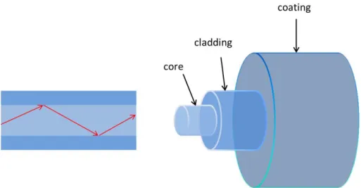
Optical fiber is a waveguide, that allows the light propagate with low loss through it in very long distances (up to kilometers). The mechanism of light propagation inside optical fiber is total reflection. The structure of optical fiber helps in understanding how light propagates in the fiber.
The cladding part has slightly lower refractive index than the core. Due to total internal reflection, the light within a certain incident angle is reflected from core-cladding interface. Therefore, the light is confined to the core. In double clad fiber, the cladding is composed of two layers, where the inner cladding is the waveguide for the pump and signal propagates inside the core. In many cases the coating functions as the second clad.
Figure 1.1: Optical fiber structure and light propagation inside it. Due to the slight difference between the refractive index of core and clad, the signal is con-fined to the core. For a typical fiber, the difference is less than 1%.
1.1.3
Lasing Principle
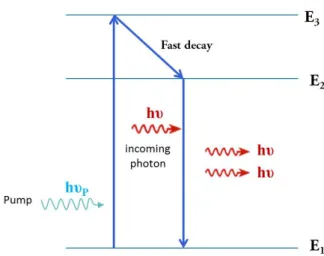
The lasing mechanism relies on the stimulated emission of excited atoms. Pump-ing provides energy for excitPump-ing atoms to higher energy levels. In order to amplify signal, it is necessary to send enough atoms to excited states, such that popula-tion inversion occurs. The excited atoms decay to lower energy levels in a time constant. A three-level system is shown in Fig. 1.2.
For a three-level system, transitions between energy levels are described in the form of rate equations [19]
dN3 dt = W (p) 13 (N1− N3) − σ32N3, (1.1a) dN2 dt = σ32N3− σ21N2+ W (s) 21 (N1 − N2), (1.1b) N1+ N2+ N3 = NEr, (1.1c)
where Wij is the probability of absorption and stimulated emission transition
Figure 1.2: Transition between energy levels in a three-level system. τ32 and τ21
are time constants of transition between the corresponding energy levels and Wp
is the pump rate.
to level j. The total atomic density in the fiber, NEr, is a constant.
From rate equations, the time constants of decaying to lower states determine the atom population at each energy level in the steady state. In most lasers, there exist three or four main energy levels. In three-level systems, most of the excited atoms accumulate in the second state. Er-doped gain fiber is a three-level system [20]. In four-level systems, the time constants are such that the majority of excited atoms accumulate in the third energy level.
In stimulated emission, signal photon stimulates an excited atom to emit an-other photon with the same phase and energy by decaying to the ground state, as shown in Fig. 1.4.
In the designed system, the gain fibers are Er-doped, for which energy dif-ference between the excited and ground state is 0.8 eV, which corresponds to a photon with 1.55 µm wavelength.
(a)
(b)
Figure 1.3: Lasing mechanism in a (a) three-level (b) four-level system. In a three-level system, the majority of atoms occupy the second energy level, while in a four-level system the atoms are mainly in E3 level.
.
1.1.4
Ultrashort Pulse Generation
So far, many methods have been introduced to generate pulses from a CW laser. Among them, mode-locking mechanism is being used to generate femtosecond pulses. In a ring cavity with the total optical length of L, the lowest frequency of the wave resonating in it is νF = c/L, where c is the light velocity. The cavity
can support the modes with frequency νq = qνF, where q is the mode number.
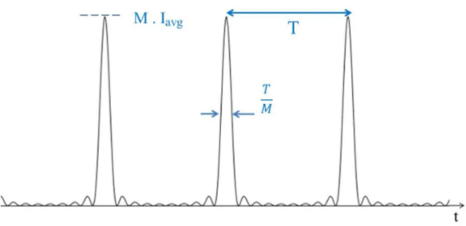
The modes oscillate independently. However, if their phase is locked together by external means, the laser is mode-locked. In this case, the modes are considered as the Fourier series components of a periodic function with period TF = 1/νF.
The light intensity coming from sum of all of the modes is a train of infinitely short pulses with period TF. However, due to gain bandwidth in the amplifier, a
finite number of modes survive. By increasing the number of phase-locked modes shorter pulse durations can be achieved. A simplified mathematical modeling for mode-lock laser is as follows. Assuming that all of the M modes supported by the cavity have magnitude A0, the complex envelope of sum of the modes can be
Figure 1.4: Photon-atom interaction resulting in stimulated emission. written as: A(t) = M X q=0 A0exp( jq2πt T ) = A0 sin(Mπt/T ) sin(πt/T ) . (1.2) The optical intensity is given by:
I(t) = |A(t)|2= A20sin
2(M πt/T )
sin2(πt/T ) , (1.3)
which is a train of short pulses, as shown in Fig.1.5.
Mode-locking techniques are generally classified to passive mode-locking and active mode-locking. In case of passive mode-locking, an essential role is played by so-called saturable absorber (SA). SA is a medium that shows lower absorption coefficient at higher intensities. Therefore, it can transmit high intensity pulses with smaller loss. Many materials and structures has been introduced as SA [21– 25]. Other than absorbing materials, one can use artificial SA. Various types of artificial saturable absorbers are completely explained in [26–28]. In our system, we used nonlinear polarization rotation by two quarter-wave plates (QWP) and one half-wave plate (HWP) as a way to passively mode-lock the laser [29].
Figure 1.5: The intensity evolution of the simplified model of a mode-locked system. The intensity is a periodic pulse function. For higher number of modes (M), the pulse duration decreases and the peak power increases.
1.1.5
Nonlinearity
Nonlinearity in the laser system appears in many faces. In fiber, due to Kerr effect, the refractive index experienced by the signal changes with the intensity. Kerr effect nonlinearity contributes to generation of short pulses in the oscillator. The light traveling in the oscillator is not of single wavelength and is composed of components within a wavelength range. Due to dispersion, the refractive index changes from wavelength to wavelength. To achieve femtosecond pulse, nonlin-earity should compensate the dispersion in the oscillator, such that in each cycle, all of the frequency components in the pulse travel with the same velocity.
Another aspect of nonlinearity, which appear in laser amplifier is gain satura-tion. As the signal intensity increases, the amplifier output power cannot follow the same output to input power ratio. In this case, nonlinearity makes it more and more difficult to build high power lasers.
1.2
Our Work
Silicon is the second most abundant element in the Earth’s crust. Showing unique electronic properties as well as its abundance has made silicon the fundamental material in electronics industry. For many applications in microelectronics, solar cell and microfluidic channels, etc. silicon needs to be processed. Silicon process-ing with laser is fast and suitable for the processprocess-ing resolution in range of mi-crometer. In the literature, numerous laser systems have been reported for silicon processing [18, 30–34]. The pulse duration in these systems vary from nanosec-ond to femtosecnanosec-ond. The light wavelengths reported in the literature are mostly less than the wavelength corresponding to silicon bandgap (1.11 µm). Since the photon energy of the light in these systems is higher than silicon bandgap energy, most of the light is absorbed by silicon. The absorption in this wavelength range is mainly a linear process. However, lasers with wavelengths longer than 1.11 µm can be used for silicon processing, too. The light absorption by silicon for such lasers is based on multiphoton absorption, which is a nonlinear process. In this process, multiple photons, mostly two photons, are absorbed simultaneously. Since silicon is transparent to the light in this range, it is possible to process the bulk of silicon. In [30], embedded patterns are generated inside silicon by a 1.55 µm nanosecond laser.
In this work, we have designed and built a master oscillator power amplifier (MOPA) Er-doped fiber laser, which can be used for silicon surface and subsur-face processing. Laser pulses have 1.5 µJ energy and 390 fs duration. The laser system generates light with 1.55 µm wavelength, to which silicon is transpar-ent. Transparency of silicon to the laser light enables us to process not only the surface, but also the bulk of silicon. The laser light in this system is absorbed via multiphoton absorption process, mostly two-photon absorption (TPA). TPA is a second order process, which is proportional to square of optical intensity. Therefore, high beam intensity favors processing. From the definition of optical intensity (I = pulse durationpulse energy×beam area), at a specific pulse energy, intensity increases as the pulse gets shorter. Consequently, in the femtosecond regime, multiphoton absorption is higher and the pulse energy required for processing is
lower than that in the nanosecond and picosecond regimes. Processing silicon via TPA mechanism also increases the ablation resolution. The absorption is proportional to I2. For a Gaussian beam with the waist w, square of the optical
intensity has a Gaussian profile with the waist √2
2 w. Hence, effective beam waist
in processing is smaller than the actual beam waist. As a result, higher processing resolution is achieved in multiphoton processing.
Chapter 2
Laser System and Measurements
The laser system is built to support sufficient pulse energy for multiphoton silicon processing. The system is composed of many stages. The pulses, which are generated in the oscillator, are stretched and then amplified in two preamplifier stages. Acusto-optic modulator (AOM) reduces the repetition rate so that we would be able to achieve high energy per pulse after the following amplifier stages. Finally, pulses are compressed to decrease the output pulse duration down to femtosecond. In this chapter, each of the aforementioned stages are discussed in detail.
2.1
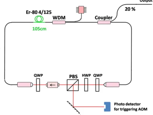
Oscillator
Basically, in the oscillator pulses are generated from a CW light pumping. The oscillator is passively mode-locked by nonlinear polarization evolution process, which is realized by a HWP, two QWPs, a polarization beam splitter (PBS) and the fibers in the cavity.
Figure 2.2: Oscillator scheme.
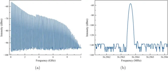
The oscillator cavity has a total optical length of 4.2 m (225 cm SMF-28 fiber, 105 cm Er-80 4/125 gain fiber and 25 cm free space), which corresponds to 59.8 MHz repetition rate. The total dispersion experienced in the cavity is -19400 fs2.
Broad and monotonically decreasing RF spectrum indicates single pulse operation and absence of oscillation. Fig. 2.3 and 2.4 show typical characteristics of the oscillator.
(a) (b)
Figure 2.3: RF spectrum of the oscillator (a) 10 GHz span (b) 1 kHz span with 10 Hz resolution. The signal to noise ratio in Fig. b is ∼ 80 dB.
Figure 2.4: Optical spectrum from oscillator. The oscillator optical spectrum has 53 nm full width half maximum (FWHM) bandwidth. The mode-lock is stable and self-starting.
The optical spectrum measured from the oscillator, which is presented in Fig. 2.4, is measured from port A in Fig. 2.5. The spectrum bandwidth is 53 nm, which corresponds to 48 fs Fourier-limited pulse duration for a sech2 pulse. Explanation
about Fourier-limited pulse can be found in Appendix A. Since the pulses obtained from the coupler (port A) are not Fourier-limited, in order to measure the shortest possible pulse duration, the dispersion should be managed. For measuring the pulse compressibility, a piece of SMF-28 and IDF stretch fiber is added. These types of fibers have opposite dispersions. The shortest pulse duration (138 fs) was achieved by manipulating the length of the two types of fibers. Pulse duration is measured by autocorrelation method, which is explained in detail in Appendix B.
Figure 2.5: Stretch fiber is spliced to the coupler output in order to compen-sate the dispersion at point A. By this technique, the pulse compressibility is investigated.
The power inside the oscillator is 94 mW. 20% of the oscillator power is given to the next stage, of which 10% goes to the oscillator monitoring port.
Figure 2.6: Autocorrelation trace of the pulse from oscillator.
2.2
Stretch Fiber, Preamplifier and Pulse Doubler
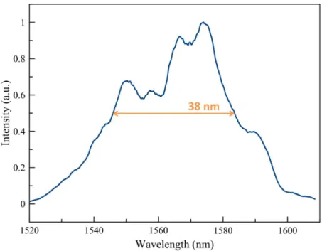
The pulse is stretched so that during amplification it experiences less non-linearity. The pulses are stretched by 300 m OFS Ocean fiber. It has negative dispersion (-44 ps/nm.km), which causes 700 ps broadening in the pulse. The spectrum bandwidth is 38 nm after stretch fiber. Unlike the fibers of the system, the stretch fiber is not polarization maintaining (PM). Therefore, a polarization controller (PC) is needed to adjust the polarization such that the maximum sig-nal power is given to the preamplifiers. In this system, the pulse is amplified in two stages before AOM. In each preamplifier stage, light at 976 nm wavelength is pumped to the gain fiber.
The stretched pulses are amplified in two stages. In the first preamplifier, the diode is driven at 800 mA current and the signal is amplified from 1.6 mW to 60 mW. The gain fiber is 1.3 m PM-ESF-7/125 Er-doped single-mode fiber. In all of the amplifier stages of this system, backward pumping is applied. Fig. 2.8
Figure 2.7: Optical spectrum after pulse stretching. depicts forward and backward pumping configurations.
In backward pumping, a potential danger is the signal diffusion into the diode, which will damage the diode. In this system, the pump wavelength (976 nm) and the signal wavelength (1.55 µm) are not close to each other. Therefore, the signal is filtered by the grating in the diode fiber and cannot pass to the diode. As a result, we can easily apply backward pumping without worrying about diode being damaged.
Backward pumping is more preferable than forward in the sense of efficiency. Its efficiency can be explained through the amplification mechanism. As the signal propagates through the gain fiber, provided that there is sufficient seed, the signal keeps getting amplified along the gain fiber. On the other hand, the pump light gets absorbed while propagating. Unlike backward pumping, in case of forward, seed and signal intensity change in opposite directions along the fiber. Hence, forward pumping is not as efficient as backward [20].
(a) (b)
Figure 2.8: Pumping the gain medium in (a) forward (b) backward configuration. In forward pumping, signal and seeds propagate in the same direction, whereas in backward case their propagation directions are opposite.
(a) (b)
Figure 2.9: Signal power along an Yb-doped fiber (blue curve) in (a) forward pumping (b) backward pumping [1]*. In forward case, the signal power saturates at some point and the gain fiber length does not affect the output power, while for backward by increasing the length of gain fiber higher power levels are attained. These curves indicate how efficient backward pumping is compared to forward. * The figures are used with the permission of the author.
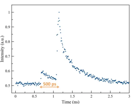
At this stage we implemented a pulse doubler. The doubler simply adds the shifted signal to the original signal. The signal is divided and guided through two paths with 10 cm length difference, which corresponds to 500 ps separation between pulses. From sampling scope measurements the pulses are 500 ps apart. Pulse doubling technique realizes ablation-cooled material removal to some extent. In ablation-cooling mechanism, intra-burst repetition rate is such that each pulse arrives before the heat from previous pulses diffuses way. According to [17] results, by increasing the number of pulses inside the burst and keeping average power unchanged, the heat affected region gets smaller and heat diffusion to the bulk of material decreases. Moreover, ablation-cooling technique increases
Figure 2.10: Pulse doubler scheme. The first coupler splits the input signal and the signal travels through two paths with different length, which gives delay to the signal. The signals from two branches are coupled back together, which gives two pulses with different amplitudes separated by desired delay value.
Figure 2.11: Doubled pulse measured by sample scope. The pulses are separated by 500 ps.
Figure 2.12: By autocorrelation the pulse duration is measured 221 fs. the ablation depth. Ideally, for achieving ablation-cooling, high number of pulses in each burst is needed. As a start, we implemented bursts of two pulses by a pulse doubler. The pulse separation is designed such that the heat deposited by the first pulse does not diffuse away before the second pulse arrives.
After pulse doubling, we built the second preamplifier. The current provided for the diode is set to 800 mA and the gain fiber is 1.5 m PM-ESF-7/125 Er-doped fiber.
2.3
AOM
Next step in this system is the AOM. AOM is an optical gate, which is controlled electronically. In this system, we used the AOM to decrease the repetition rate from 60 MHz to 905 kHz. It is triggered by the oscillator signal. The beam
coming from the PBS port inside oscillator is detected by a photodetector.
Figure 2.13: AOM and FPGA connections. The FPGA is programmed such that from every 66 oscillator the AOM transmits 1 pulse.
The FPGA is programmed such that from each 66 pulses of the oscillator, one of them is transmitted through the AOM.
The reason behind reducing repetition rate is that we need to achieve higher pulse energies. For instance, in the case of silicon surface processing, pulse energy is one of the most determinative parameters. By decreasing repetition rate, the power is distributed between fewer pulses and the pulse energy increases. How-ever, at small repetition rate values, undesired phenomena such as high amplified spontaneous emission (ASE) get considerable. The system repetition rate is such that none of these undesired phenomena play a significant role.
2.4
Amplifiers
After the AOM, the pulses are amplified in three stages. The third preamplifier is pumped by a low power diode. The diode is driven at 1000 mA current. The signal is amplified in 1.5 m PM-ESF-7/125 gain fiber. As mentioned before, for the sake of efficiency, all the amplifier stages in this system use backward pumping. In this stage, the power level increases from 0.7 mW to 50 mW.
Figure 2.14: Pulses after the AOM. The repetition rate is reduced to 905 kHz. stage, the power level is designed to be high. At high optical intensities, the light propagating in the fiber experiences strong nonlinearity. To avoid nonlinearity issue, we need to use fiber with larger core size, so that light intensity decreases. However, larger core give rise to undesired transverse modes. The fiber has 12 µm core diameter. The beam propagating in this fiber is still single-mode. The gain fiber is a double clad DCF-EY-12/130 fiber. In a double clad fiber, the signal propagates inside the core, while the pump is launched to the inner cladding. The outer cladding has lower refractive index, which makes the pump confined to the inner cladding.
The laser diode is driven by a high power laser diode driver (PLD10000), which can supply up to 10 A current. The diode current is set to 2.6 A, which pumps 2.8 W to the gain fiber. Instead of wavelength-division multiplexer (WDM), which was used in previous stages, in this stage the signal and seed are mixed in a multi-mode pump combiner (MPC).
Figure 2.15: Optical spectrum bandwidth after third preamplifier is 16 nm. The signal power is increased to 500 mW in this stage. However, the optical spectrum bandwidth decreases to 8 nm.
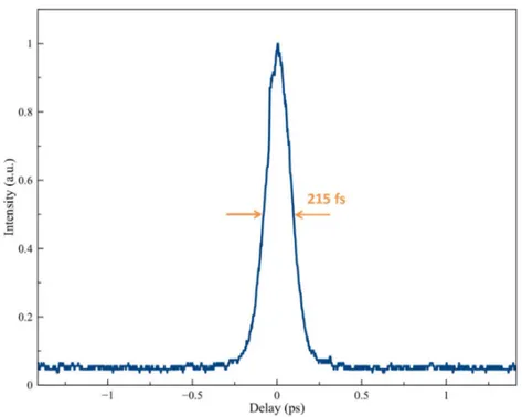
In this step, the pulse compressibility was investigated. For this purpose, we used parallel grating compressor, which is described in the next section thor-oughly. The FWHM of autocorrelation result is 450 fs, which correspond to 290 fs duration of the original pulse. However, there is a pedestal in the autocorrelation trace.
Finally, in the last stage the signal is amplified to reach full power. The pump diode is driven at 6.6 A current, which pumps 16 W to the gain fiber. All the fibers used in final amplifier stage are double clad. Moreover, due to the high power level, the splice point between gain fiber and combiner would radiate too much heat and it would be prone to get damaged in the long term. To prevent damage to the system, in final amplifier stage free-space pumping is applied.
Figure 2.16: Pump and signal propagation in a double clad fiber in backward pumping. The pump light propagates in the cladding, while the signal light is confined to the core of the fiber.
Figure 2.18: Autocorrelated trace before final amplifier.
Figure 2.19: Free-space backward pumping setup. The 915 nm light coming from the diode is collimated and transmitted through the dichroic mirror and is focused on the gain fiber tip. It propagates in gain fiber and amplifies the signal coming from the previous stage. The amplified 1550 nm light is then reflected from the dichroic mirror.
For improving the beam shape, a connector fiber with respectively 20 µm and 125 µm core and clad size is used. The clad and core size of the connector is close to isolator cladding size and gain fiber core size respectively.
Figure 2.20: The technique for connecting fibers with different sizes. A connector fiber with core and clad size close to core of one fiber and clad of the other fiber eases splicing.
For further improvement in the beam shape, we apply fiber tip polishing. Unlike thin fibers, for relatively thick fibers cleaving is not enough. The tip of the cleaved fiber is not smooth. The tip roughness causes light being scattered in the splice point, which leads to undesired beam shape. To avoid this problem, the tip is polished. By tip polishing, we managed to get a circular beam in the output.
Final amplifier stage generates 2 W power in the output. The spectrum band-width is 11 nm for the output light.
As it can be seen, in the final amplifier the pulses of the doubler have almost same intensity ratio as their ratio right after doubler. The separation between the pulses has not changed during propagation toward final stage. At first glance it may seem to contradict the Kerr effect, since the refractive index for the stronger pulse is higher and hence it should propagate slower. Consequently, the pulse separation is expected to increase. The point is that Kerr effect in this case does not affect the refractive index considerably. The intensity difference of the pulses is in the order of 109 W/cm2 and the Kerr nonlinearity (n
2) is 5 × 10⁻¹⁴
cm2/W [38]. The doubled pulses travel 10 m, which increases the pulse separation
by less than 10 ps. This value is negligible compared to the initial separation (500 ps).
Figure 2.21: Amplified doubled pulse in the output.
2.5
Compressor
While propagating in the stretch fiber the light experiences normal dispersion, which means longer wavelength components propagate faster. From temporal point of view, the pulse will get broader and broader. To compensate the broad-ening, the pulse needs to have negative dispersion in the compressor. The com-pressor consists of two diffraction gratings and one mirror. Between gratings, the light is dispersed such that the longer wavelengths travel longer distance. Hence, we can manage to compress the pulse to the shortest duration possible (not nec-essarily to its Fourier limit) by adjusting the separation between the gratings.
The gratings have 900 lines/mm. To get maximum efficiency at 1550 nm, the incident beam angle to the gratings should be 30◦ . Besides, the grating
grooves separation (1.1 µm) is smaller than the light wavelength. Under this condition, the power transmitted through grating is polarization dependent. A HWP before first grating changes the polarization such that the diffracted light
Figure 2.22: Pulse compression. The light is diffracted once at parallel grating. A large golden mirror, on which the diffracted beam fits, reflects the light. The gratings and the mirror are aligned such that the beam travels back on the same path.
has maximum power. By rotating HWP, we minimize the power of the beam transmitted from the first grating. By rotating the first grating we maximized the power reached to the second grating. To make sure the gratings are parallel, we rotate the second grating until the power transmitted through it gets minimum. From dispersion calculations the normal distance between gratings should be 86 cm. By moving the second grating on a translation stage the separation between gratings is adjusted such that the shortest pulse is obtained in the output.
The FWHM of the autocorrelation result is 600 fs, which corresponds to 390 fs pulse duration.
Figure 2.23: Optical spectrum of output signal.
Figure 2.24: Autocorrelation trace of the output pulse. The FWHM of autocor-relation trace corresponds to 390 fs pulse duration.
2.6
Beam Quality
The beam quality can be obtained from the M2 parameter of the beam. This
parameter shows how close the beam is to a single-mode (TEM00) beam. In
this method, a beam profiler measures the beam radius at different z positions including the waist, where the beam size is the smallest. Then a Gaussian curve is fitted to the measured values and theoretical beam waist is obtained from the curve. Finally, M2 parameter is obtained from the equation
M2 = (Dm d0
)2, (2.1)
where Dm and d0 are measured and theoretical beam waist respectively. In our
measurement, the M2 parameter is evaluated in two axes perpendicular to
prop-agation direction. For the output beam, the M2 parameter is measured 1.36 and
1.50 in the perpendicular axes, which gives average value of 1.43. However, it is difficult to get small M2 value at higher power levels. The reason behind it
is that at high power transverse modes as well as parasitic effects appear, which causes the beam to lose its circular shape.
Figure 2.25: Beam quality measurement. Each of the beam profiles in x and y directions (plotted in yellow) are compared to a Gaussian profile (red).
2.7
ASE Measurement
In the gain medium, some of the active ions emit spontaneously [20]. This emis-sion is amplified in the gain medium, which is called ASE. As a result of high ASE, the gain saturates [20]. Moreover, ASE strongly depends on repetition rate [35]. At low repetition rates, one of the challenges is to reduce ASE. The ASE from each stage is amplified in following stages. Therefore, the most effective approach for reducing the ASE in the output is to eliminate ASE step by step, starting from earlier amplifier stages. One of the most common methods for reducing ASE is to pump seeds only when there is signal rather than CW pumping. This technique is called pulse pumping. By choosing appropriate timing for the pumped pulse, the ASE gets suppressed [35]. In our system, the ASE ratio is measured 0.7% at 905 kHz repetition rate. The setup shown in Fig. 2.26 is used to measure ASE.
Figure 2.26: ASE measurement setup. The signal generator is triggered by the oscillator pulses and generates a square wave, which closes the AOM when the pulse is arriving. With this method the power from ASE is measured. In the case of full transmission of the AOM, the total power is measured. The AOM used for ASE measurement cannot tolerate high power. Therefore, we need to lower the power. The pair of HWP and PBS can adjust the power such that the AOM is not damaged.
Chapter 3
Silicon Surface Processing
3.1
Ablation Mechanism
Ablation mechanism strongly depends on the pulse duration. In the CW and nanosecond regime, the ablation is a thermal process, which occurs as a result of direct vaporization. The laser beam deposits energy in a shallow layer in the material. Since the pulse duration in this regime is much longer than thermal conduction time, much of the pulse energy is thermally conducted to the regions around the beam spot. The temperature in the beam spot is so high that the material melts. Continuous application of laser causes the substrate to vaporize [31].
In the long pulse regime, the ablation precision is not high. The mechanical shock due to solid-liquid-vapor phase change causes stress in the material [36]. The material processing precision decreases as a result of formation of vapor and liquid phases in the vicinity of the beam spot. In the picosecond regime, the processing precision is higher than the microsecond and nanosecond pulse regimes [33].
diffusion time constant. In this case, relatively little heat diffuses away from the beam spot, which can be further reduced by ablation-cooling [17]. Ablation-cooling mechanism increases the ablation rate drastically. To get a better intu-ition of femtosecond ablation mechanism, ablation process and the related char-acteristic time constants need to be mentioned. Laser photons couple with the state of electrons in the valance band and conduction band. The deposited en-ergy is distributed in the system mainly by carrier-carrier, carrier-phonon and phonon-phonon interaction. The energy relaxation time is the time duration for reaching thermal energy distribution, namely Fermi-Dirac function for electrons and Bose-Einstein for photons. For semiconductors and metals, the relaxation time constants are typically in the range of 10−11 to 10−12 s. Therefore, for most
of materials the femtosecond pulse affects long before the matter reaches thermal equilibrium [37].
3.2
Ablation Threshold
The minimum intensity required for material ablation is called ablation threshold (ΦTH). For intensities below ablation threshold, the temperature is not high
enough to ablate material. However, in some materials, insufficient intensity can accelerate oxidation. Depending on the laser fluence, different morphological processes may occur. By increasing the laser fluence, oxidation, amorphization, re-crystallization, bubbling due to subsurface boiling and finally ablation occur respectively [32].
Ablation threshold for a specific material depends on many parameters. It de-pends on the incident wavelength, because the photon absorption of the material changes with wavelength. Even the absorption mechanism (single photon or mul-tiphoton absorption) may change from one wavelength to another, which will be discussed in the next section in detail. ΦTH depends on the pulse duration, too.
For shorter pulse durations, the whole pulse energy is deposited in the laser spot before it can diffuse away to the lattice, which leads to smaller ablation threshold
for ultrashort pulses. Intuitively, the ablation occurs as a result of energy ac-cumulation in the processing spot. In other words, thermal memory determines if the material ablation occurs. Based on this fact, different techniques can be applied to reduce the ablation threshold. Increasing the repetition rate helps the new pulse benefit from the heat remaining from previous pulses, which eases ab-lation [17]. This concept can be realized by burst-mode operation of laser, where intra-burst repetition rate is high.
Figure 3.1: Burst-mode operation of laser. The burst period is typically much larger than the burst duration.
This technique, known as ablation-cooled material removal, decreases the min-imum pulse energy required for ablation. Besides, since the heat diffusion is elim-inated, the ablation precision increases [17]. Other than laser parameters, the lattice orientation changes the threshold. For instance, the threshold for silicon ablation on < 111 > plane is smaller [34].
3.3
Two-Photon Absorption in Silicon
In semiconductors, electrons are excited by absorption of photons and occupying empty states in the conduction band, as shown in Fig. 3.2.
However, even if the photon energy is smaller than the semiconductor bandgap energy, the electrons can get excited via multiphoton absorption (MPA) process. The bandgap energy in silicon is 1.12 eV, which corresponds to 1.1 µm wavelength.
Figure 3.2: Band structure in semiconductors. Electrons from the valance band can occupy an empty state in the conduction band by absorbing a photon with enough energy.
Thus, for the photons with wavelength longer than 1.1 µm the absorption in silicon is through MPA. Beer-Lambert Law gives the light intensity for a two-photon absorbing material along the propagation direction x.
I(x) = I0 1 + βxI0
, (3.1)
where I0 is the initial intensity. The absorption is defined as the derivative of the
intensity.
−dI dx = βI
2. (3.2)
From [38], the TPA coefficient (β) of silicon at 1.55 µm wavelength is 1.3 cm/GW. TPA increases with the square of the intensity. By definition, intensity is the power applied to unit area. For a pulsed laser, intensity can be written as:
I = E
∆t × A, (3.3)
where E is the energy per pulse, ∆t is pulse duration and A is the spot size. Clearly at a fixed pulse energy, the intensity and thus TPA increases as the pulse gets shorter. Strong dependence of absorption to intensity suggests application of ultrashort laser in material multiphoton processing.
3.4
Surface Processing
In this section, the surface processing setup is explained.
Figure 3.3: Surface processing setup.
Since ablation in our experiment is based on TPA, high beam intensity is needed in order to increase TPA. For this purpose, a lens with 12.5 mm focal length is used to focus the beam on the surface. The laser output beam is a highly collimated Gaussian beam. For a focused beam at wavelength λ, the
Figure 3.4: Gaussian beam width along the propagation direction. The beam is focused by a lens with focal length f. θ is the beam divergence angle, 2a is the width of the collimated beam and 2w0 is the focused beam diameter.
beam diameter can be calculated from the formula 2w0 =
2M2λ
where
θ = tg−1(a
f). (3.5)
From beam measurement, the laser beam waist before focusing is measured 180 µm, which gives 19.6 µm beam diameter for the light focused on the surface. In our experiment, p-type silicon with the resistivity of 1-10 Ω/cm and the thickness of 500 µm is used. The silicon sample is mounted on a translation stage and held fixed by two magnets on each side. The motorized translation stage is controlled by computer interface. To focus the beam exactly on the surface, we move the stage back and forth, until intensity of white sparks gets maximum. The white spark is due to plasma, which forms when beam with sufficient intensity ablates silicon. The surface is scanned along x direction with 0.3 mm/s speed (Fig. 3.3). The laser beam makes trench on the surface. The experiment is repeated at different pulse energies.
Chapter 4
Ablation Measurements and Results
The processed samples are prepared for measurement. Sample preparation pro-cess includes HF etching followed by acetone cleaning. Afterwards, the trenches generated by the laser beam are characterized by different equipment.
4.1
Chemical Etching
During processing, silicon particles splatter around, both inside the trench and on the surface. Since the temperature at the laser spot is very high, the splattered particles are easily oxidized. The measurement results would be misleading if the oxide piles are not removed from the sample. For this purpose, the sample is chemically etched in HF acid. The etch rate for silicon is much lower than the oxide. Therefore, during oxide etching silicon remains almost untouched. The sample is kept in diluted HF acid for 10 minutes to remove oxide. The acid is thinned with deionized water by 1:15 ratio.
4.2
SEM Imaging
Scanning electron microscope (SEM) imaging is a very common method to inves-tigate the sample after any fabrication process. In a SEM microscope, a beam of electron is accelerated toward the sample. The electrons scattered from the sample produce signals containing information about surface topography, com-position, etc. In this work, SEM imaging is utilized for observing the sample topography after laser processing. Fig. 4.1 shows the SEM image of the channel cross section.
(a) (b)
Figure 4.1: The cross section of the trench generated at laser full power (1.3 W) observed by a SEM microscope with the magnification scale (a) 1200X (b) 3700X. As discussed on ablation threshold in chapter 3, insufficient pulse energy leads to oxidation instead of ablation. By comparing the SEM images of etched and not-etched sample, it is investigated if the material is ablated or just oxidized. However, this method cannot investigate ablation accurately. For instance, the silicon particles splattered during ablation may fill the trench and cannot be distinguished from the oxidized region during processing. Moreover, it is possible that both ablation and oxidation occur during processing. The energy deposited very close to the surface causes ablation and the energy diffused into the bulk oxidizes the exposed silicon bulk.
(a) (b)
Figure 4.2: SEM image of the trench generated at 1 W output power (a) before etching (b) after etching. By comparing the images it can be understood that the surface is ablated rather than being merely oxidized.
(a) (b)
(c) (d)
Figure 4.3: SEM image of the processed area at output power of (a) 0.9 W (b) 1 W (c) 1.1 W (d) 1.15 W.
4.3
Profilometry
After etching, the trench depth is measured using 3D optical profilometer Zygo 7200. The smallest structures detected by optical profilometers are in the range of hundreds of nanometers, whereas in mechanical profilometers the resolution is smaller. In mechanical profilometers, the resolution limit is due to the scanning tip. The tip size is typically in the range of few micrometers, which makes it impossible to get profile of the structures smaller than few micrometers. The optical profilometer gives the sample profile as well as 3D view of the surface. The colors in the 3D image represent depth of the trench.
(a) (b)
(c) (d)
Figure 4.4: 3D view of the trenches generated at (a) 0.9 W (b) 1 W (c) 1.1 W (d) 1.15 W output power. In figure (c) there exist two trenches. The right trench is generated while the beam was not focused on the sample completely and only the left one is included in the measurements.
(a) (b)
(c) (d)
Figure 4.5: Top view of the trenches generated at (a) 0.9 W (b) 1 W (c) 1.1 W (d) 1.15 W output power.
In order to measure the channel depth, profilometer scans the surface along the specified line. The depth at each point on the line is measured.
(a) (b)
(c) (d)
Figure 4.6: Profile of the channels generated at (a) 0.9 W (b) 1 W (c) 1.1 W (d) 1.15 W output power.
Chapter 5
Conclusion
In this thesis, we investigated the possibility of multiphoton silicon surface pro-cessing with femtosecond fiber laser. For this purpose we designed and built an Er-doped femtosecond fiber laser with MOPA architecture. Due to the all-fiber-integrated design, the system is stable, robust and free of misalignment. The laser beam is always confined in a fiber or fiberized component at all points (ex-pect in final amplifier), which causes immunity to mechanical perturbation. In summary, the system provides 1.3 W average power at 905 kHz repetition rate, which corresponds to 1.5 µJ energy per pulse. The beam shape is nearly single-mode (M2 = 1.43). Minimum pulse duration at 1.5 µJ of pulse energy is 390 fs
FWHM. The laser system was successfully applied for silicon surface processing through TPA mechanism. In two-photon processing, the effective beam size is smaller than single-photon case, which makes it possible to achieve higher pro-cessing resolution. The results from surface propro-cessing suggest that the channel depth increases as the output power and hence pulse energy increases. Along with ablation, oxidation occurs inside and outside the trench, which is etched by HF acid before trench characterization.
To the best of our knowledge, this is the first demonstration of silicon surface processing with 1.5 µm femtosecond laser, where the initial absorption mechanism is TPA. We expect this technique to find many industrially and scientifically
important applications including solar cell technology, micro- and nanoelectronics and biomedical applications.
Bibliography
[1] R. Paschotta, “Encyclopedia of laser physics and technology of RP Photonics, tutorial on fiber amplifiers.” https://www.rp-photonics.com/tutorial_ fiber_amplifiers5.html.
[2] F. Beier, H.-J. Otto, C. Jauregui, O. de Vries, T. Schreiber, J. Limpert, R. Eberhardt, and A. Tünnermann, “1009 nm continuous-wave ytterbium-doped fiber amplifier emitting 146 W,” Optics Letters, vol. 39, no. 13, pp. 3725–3727, 2014.
[3] P. Elahi, S. Yılmaz, Y. B. Eldeniz, and F. Ö. Ilday, “Generation of picosecond pulses directly from a 100 W, burst-mode, doping-managed Yb-doped fiber amplifier,” Optics Letters, vol. 39, no. 2, pp. 236–9, 2014.
[4] F. Stutzki, C. Gaida, M. Gebhardt, F. Jansen, C. Jauregui, J. Limpert, and A. Tünnermann, “Tm-based fiber-laser system with more than 200 MW peak power,” Optics Letters, vol. 40, no. 1, pp. 9–12, 2015.
[5] R. A. Delgado-Ruiz, J. L. Calvo-Guirado, P. Moreno, J. Guardia, G. Gomez-Moreno, J. E. Mate-Sanchez, P. Ramirez-Fernandez, and F. Chiva, “Fem-tosecond laser microstructuring of zirconia dental implants,” Journal of Biomedical Materials Research - Part B Applied Biomaterials, vol. 96 B, no. 1, pp. 91–100, 2011.
[6] K. E. Donaldson, R. Braga-Mele, F. Cabot, R. Davidson, D. K. Dhaliwal, R. Hamilton, M. Jackson, L. Patterson, K. Stonecipher, and S. H. Yoo, “Fem-tosecond laser-assisted cataract surgery,” Journal of Cataract and Refractive Surgery, vol. 39, no. 11, pp. 1753–1763, 2013.
[7] J. Bonse, J. Krüger, S. Höhm, and A. Rosenfeld, “Femtosecond laser-induced periodic surface structures,” Journal of Laser Applications, vol. 24, no. 4, p. 042006, 2012.
[8] B. Öktem, I. Pavlov, S. Ilday, H. Kalaycıoğlu, A. Rybak, S. Yavaş, M. Er-doğan, and F. Ö. Ilday, “Nonlinear laser lithography for indefinitely large-area nanostructuring with femtosecond pulses,” Nature Photonics, vol. 7, no. 11, pp. 897–901, 2013.
[9] H. Keskin, H. Altan, S. Yavaş, F. Ö. Ilday, K. Eken, and A. B. Sahin, “De-velopment of a rapid-scan fiber-integrated terahertz spectrometer,” Optical and Quantum Electronics, vol. 46, no. 4, pp. 495–503, 2014.
[10] M. Deubel, G. von Freymann, M. Wegener, S. Pereira, K. Busch, and C. M. Soukoulis, “Direct laser writing of three-dimensional photonic-crystal tem-plates for telecommunications,” Nature Materials, vol. 3, no. 7, pp. 444–447, 2004.
[11] C. L. Hoy, O. Ferhanoğlu, M. Yıldırım, K. H. Kim, S. S. Karajanagi, K. M. C. Chan, J. B. Kobler, S. M. Zeitels, and A. Ben-Yakar, “Clinical Ultrafast Laser Surgery: Recent Advances and Future Directions,” IEEE Journal of Selected Topics in Quantum Electronics, vol. 20, no. 2, pp. 242–255, 2014.
[12] S. H. Chung and E. Mazur, “Surgical applications of femtosecond lasers,” Journal of Biophotonics, vol. 2, no. 10, pp. 557–572, 2009.
[13] A. Plech, V. Kotaidis, M. Lorenc, and J. Boneberg, “Femtosecond laser near-field ablation from gold nanoparticles,” Nature Physics, vol. 2, no. 1, pp. 44– 47, 2005.
[14] R. R. Gattass and E. Mazur, “Femtosecond laser micromachining in trans-parent materials,” Nature Photonics, vol. 2, no. 4, pp. 219–225, 2008. [15] F. Loesel, J. Fischer, M. Götz, C. Horvath, T. Juhasz, F. Noack, N. Suhm,
and J. Bille, “Non-thermal ablation of neural tissue with femtosecond laser pulses,” Applied Physics B: Lasers and Optics, vol. 66, no. 1, pp. 121–128, 1998.
[16] T. Juhasz, F. H. Loesel, R. M. Kurtz, C. Horvath, J. F. Bille, and G. Mourou, “Corneal refractive surgery with femtosecond lasers,” IEEE Journal of Se-lected Topics in Quantum Electronics, vol. 5, no. 4, pp. 902–910, 1999. [17] C. Kerse, H. Kalaycioğlu, P. Elahi, B. Çetin, D. K. Kesim, O. Akçaalan,
S. Yavaş, M. D. Aşık, B. Öktem, H. Hoogland, R. Holzwarth, and F. O. Ilday, “Ablation-cooled material removal with ultrafast bursts of pulses,” Nature, vol. 537, pp. 84–88, 2016.
[18] C. Kerse, Ablation Cooled Material Removal With Bursts of Ultrafast Pulses. PhD thesis, Bilkent University, 2016.
[19] I. Pavlov, E. Dülgergil, E. Ilbey, and F. O. Ilday, “Diffraction-limited, 10-W, 5-ns, 100-kHz, all-fiber laser at 1.55 µm,” Optics Letters, vol. 39, pp. 2695– 2698, May 2014.
[20] R. Paschotta, Field Guide to Optical Fiber Technology. SPIE, Washington, 2010.
[21] S. Y. Set, H. Yaguchi, Y. Tanaka, and M. Jablonski, “Laser Mode Locking Using a Saturable Absorber Incorporating Carbon Nanotubes,” Journal of Lightwave Technology, vol. 22, no. 1, pp. 51–56, 2004.
[22] A. Martinez and S. Yamashita, “Multi-gigahertz repetition rate passively modelocked fiber lasers using carbon nanotubes.,” Optics Express, vol. 19, no. 7, pp. 6155–6163, 2011.
[23] Q. Bao, H. Zhang, Y. Wang, Z. Ni, Y. Yan, Z. X. Shen, K. P. Loh, and D. Y. Tang, “Atomic-layer graphene as a saturable absorber for ultrafast pulsed lasers,” Advanced Functional Materials, vol. 19, no. 19, pp. 3077–3083, 2009. [24] F. X. Kärtner, I. D. Jung, and U. Keller, “Soliton mode-locking with sat-urable absorbers,” IEEE Journal on Selected Topics in Quantum Electronics, vol. 2, no. 3, pp. 540–556, 1996.
[25] F. J. Grawert, J. T. Gopinath, F. O. Ilday, H. M. Shen, E. P. Ippen, F. X. Kärtner, S. Akiyama, J. Liu, K. Wada, and L. C. Kimerling, “220-fs erbium-ytterbium: glass laser mode locked by a broadband low-loss sili-con/germanium saturable absorber,” Optics Letters, vol. 30, no. 3, pp. 329– 331, 2005.
[26] H. A. Haus, J. G. Fujimoto, and E. P. Ippen, “Analytic Theory of Additive Pulse and Kerr Lens mode Locking,” IEEE Journal of Quantum Electronics, vol. 28, no. 10, pp. 2086–2096, 1992.
[27] J. Herrmann, “Theory of Kerr-lens mode locking: role of self-focusing and radially varying gain,” Journal of the Optical Society of America B, vol. 11, no. 3, p. 498, 1994.
[28] P. Elahi, I. L. Budunoglu, K. Gürel, and F. Ilday, “Laser oscillator with non-linear saturable absorber: A pump to signal noise transfer function model,” in Nonlinear Optics, p. NWE20, Optical Society of America, 2011.
[29] S. Yavaş, Ultrashort and Short Pulsed Fiber Laser Development for Trans-parent Material Processing, Imaging and Spectroscopy Applications. PhD thesis, Bilkent University, 2015.
[30] O. Tokel, A. Turnali, I. Pavlov, S. Tozburun, I. Akca, and F. O. Ilday, “Laser-writing in silicon for 3D information processing,” 2014.
[31] J. Y. J. Jia, The Mechanism of Thin Film Si Nanomachining Using Fem-tosecond Laser Pulses. Master thesis, Massachusetts Institute of Technology, 2004.
[32] J. Bonse, S. Baudach, J. Krüger, W. Kautek, and M. Lenzner, “Femtosecond laser ablation of silicon-modification thresholds and morphology,” Applied Physics A: Materials Science & Processing, vol. 74, no. 1, pp. 19–25, 2002. [33] B. N. Chichkov, C. Momma, S. Nolte, F. von Alvensleben, and A.
Tünner-mann, “Femtosecond, picosecond and nanosecond laser ablation of solids,” Applied Physics A: Materials Science & Processing, vol. 63, no. 2, pp. 109– 115, 1996.
[34] J. A. Yater and M. O. Thompson, “Orientation dependence of laser amor-phization of crystal Si,” Physical Review Letters, vol. 63, pp. 2088–2091, 1989.
[35] H. Kalaycioglu, Ö. Akçaalan, S. Yavas, Y. B. Eldeniz, and F. O. Ilday, “Burst-mode Yb-doped fiber amplifier system optimized for low-repetition-rate operation,” Journal of the Optical Society of America B, vol. 32, no. 5, p. 900, 2015.
[36] D. Kim, M. Ye, and C. Grigoropoulos, “Pulsed laser-induced ablation of ab-sorbing liquids and acoustic-transient generation,” Applied Physics A: Ma-terials Science & Processing, vol. 67, pp. 169–181, 1998.
[37] D. von der Linde and K. Sokolowski-Tinten, “The physical mechanisms of short-pulse laser ablation,” Applied Surface Science, vol. 154, pp. 1 – 10, 2000.
[38] A. D. Bristow, N. Rotenberg, and H. M. van Driel, “Two-photon absorption and Kerr coefficients of silicon for 850-2200 nm,” Applied Physics Letters, vol. 90, no. 19, pp. 16–18, 2007.
Appendix A
Fourier-limited Pulse
For describing a pulse of light we start from a monochromatic plane wave.
E(r, t) = E0ei(k.r−ωt). (A.1)
As we know, in the light pulse we deal with a continuum of frequencies rather than a single frequency. The frequencies included in the light pulse are related to the electric field by Fourier transform.
˜ E(ω) =
Z +∞
−∞
E(t)eiωtdt. (A.2) Since electric field is a complex function, it is more convenient to deal with the square of electric field magnitude (|f|2), which is a real function.
For convenience, we treat envelope function in a purely mathematical sense. The electric field envelope is described in both time and frequency domain, i.e. f (t) and ˜f (ω) respectively. The width of the functions at half their maximum values is represented by δt and δω. Since f(t) and ˜f (ω) are related through Fourier transform, δt and δω are not independent.
Figure A.1: Pulse envelope (|E|2) and real part of the complex electric field E(t).
Figure A.2: An arbitrary pulse with duration δt and corresponding spectrum with bandwidth δω. δt and δω are limited by each other. A pulse with a specific bandwidth cannot be shorter than a certain value.
optical spectrum. For a given optical spectrum the lowest pulse duration is re-garded as Fourier limit. In case the spectral phase is frequency-independent, which results in pulse without chirp, the time-bandwidth product is minimum and the pulse is Fourier-limited. For a Fourier-limited pulse the time-bandwidth product depends on the envelope function. Table A.1 contains time-bandwidth product for typical optical pulse functions. The pulse duration in all the cases is δt.
In general, for an arbitrary spectrum I(f), the corresponding Fourier-limited pulse shape I(t) is easily derived from the inverse Fourier transform.
Envelope Function f (t) f (ω)˜ Time-Bandwidth Product Hyperbolic Secant A sech (2t
α) A 0sech ( πωδt 4log(1+√2)) 0.31 Gaussian A exp(−t2 2τ2) A0exp( −ω2δt2 8log2 ) 0.44 Lorentzian A 1+α2t2 A 0exp( −|ω|δt 2 √√ 2−1) 0.22
Table A.1: Time-bandwidth product and Fourier transform of typical pulse func-tions.
FWHM of I(t) gives the minimum possible pulse duration for the pulse with frequency spectrum I(f). However, if the phase is frequency dependent and hence the pulse is chirped, the pulse is not transform limited anymore. In such a case the pulse duration is larger than FWHM of I(t).
Appendix B
Pulse Duration Measurement
Through Autocorrelation
For measuring a event in time a shorter event is required. Ultrashort pulses are too short to be detected by any optoelectronic detector. Hence, the pulse is used to measure itself. Optical autocorrelation is a common technique for measuring femtosecond pulse duration.
Mathematically, autocorrelation is a measure of how similar is the signal with its delayed version. For signal f(t), autocorrelation is defined as:
A(τ ) = Z ∞
−∞
f (t).f∗(t − τ )dt, (B.1) where f∗ is the complex conjugate of f.
In this technique the beam splits into two part, one of which travels a variable distance, while the path for the other one is fixed.
The pulses are delayed by τ. The path lengths are set such that by rota-tion of the disk τ swings symmetrically around zero. The two beam lights are then focused and overlapped inside a second harmonic generator (SHG) crystal. For the complex electric field E(t) SHG crystal generates signal proportional to E2(t) + E(t). In intensity autocorrelator (also known as second order