THE PHOTOVOLTAIC CHARACTERIZATION OF MO/METHYLENE BLUE/N-SI/ AL/AU CONTACTS
Omar Muhammed TAHSEEN MASTER THESIS Department of Physics
Supervisor: Asst. Prof. Dr. Kadir EJDERHA May 2017
INSTITUTE OF SCIENCE
THE PHOTOVOLTAIC CHARACTERIZATION OF
MO/METHYLENE BLUE/N-SI/ AL/AU CONTACTS
MASTER THESIS
Omar Muhammed TAHSEEN
Department: PHYSICS
Supervisor: Asst. Prof. Dr. Kadir EJDERHA
INSTITUTE OF SCIENCE
THE PHOTOVOLTAIC CHARACTERIZATION OF MO/METHYLENE
BLUE/N-SI/ AL/AU CONTACTS
MASTER’S THESIS
Omar Muhammed TAHSEEN
Department Institute : PHYSICS
This thesis was unanimously approved by the following jury on 23.05.2017
Prof. Dr. Abdulmecit TÜRÜT Prof. Dr. Nezir YILDIRIM Asst. Prof. Dr. Kadir EJDERHA
President of the Jury Member Supervisor
I confirm the result above Prof. Dr. İbrahim Y. ERDOĞAN
i
Everyone has some things in the world, people who value and value the world, But I am favourite is my family. They are very important for my life, one by one, my parent’s mom Dimeen Jallal and dad Muhammed Tahseen, brothers Mustafa and Muthana , sister Hiba and dear wife Zhyawa Muhseen and support me all the relative, Thank you I was always there, I thanks your for supporting me, I love you all.
ii
PREFACE
Firstly, I would like to express my gratitude to my advisor Asst. Prof. Dr. Kadir Ejderha for sharing his valuable experiences, his guidance and support during my research. Also I would like to thank all members of friends working in the lab, I must also thank to I received training all teachers for his generous help at the essential part of my research Dr. Tariq. Thank you very much dear my parents, brothers, sister and dear wife and support me all the tumors thank you thank you. I would like to thanks my close friends and my beloved friends Uğur BAĞCI, Abdullah BEKİL, Bilal OTHMAN for their moral support.
Omar Muhammed TAHSEEN Bingöl 2017
iii
PREFACE ... ii
CONTENTS ………... iii
ABBREVIATIONS... v
LIST OF SYMBOLS... vii
LIST OF TABLES... ix
LIST OF FIGURES ... x
ÖZET ………... vii
ABSTRACT ... xiii
1. INTRODUCTION ……….. 1
2. THE LITERATURE REVIEW ………... 6
3. TEORY ……….……… 10
3.1. Solar Cells ……….………. 10
3.1.1. Types of Solar Cells ……...……….. 10
3.1.2. Working Principle of Solar Cells ………. 10
3.2. Solar Energy ……...……… 11
3.3. Solar Radiation………...……… 12
3.4. Fundamentals of Semiconductor Physics ………….……….. 13
3.4.1. Bohr Model………...……… 13
3.4.2. Energy Bands of Semiconductors………. 14
3.4.2.1. Energy band diagrams of common semiconductors………... 15
3.4.2.2. Simple energy band diagram of a semiconductor………... 15
3.4.2.3. Temperature and doping dependence of the energy bandgap………. 16
3.5. Semiconductors……….……. 16
3.5.1. n-type Semiconductors……….………..…. 17
3.6. Light Absorption into and Electron Extinction out of a Semiconductor………... 17
3.6.1. Photon Absorption Coefficient……… 18
3.6.2. Electron–Hole Pair Generation Rate……… 19
3.7. Metal Semiconductor Contacts………...… 20
3.7.1. Metal–Semiconductor Ohmic Contact………. 20
iv
4.2. Rotation (spinning) Film Coating Technique………. 32
4.3. Annealing Furnace ……… 33
4.4. Characterization Procedure………...………. 34
4.5. The cross-sectional SEM image………. 45
5. RESULTS AND DISCUSSION……… 47
v ABBREVIATIONS Ag Al AM Ar Au C CdTe CIGS CNT CVD CZTS DC eV FF Ga GLAD GW I In ITO kW Mo MPP MW n-Si N2 NW : Silver : Aluminium : Air Mass : Argon gas : Gold : Carbon : Cadmium Telluride
: Copper Indium Gallium Selenide : Carbon Nano Tube
: Chemical Vapor Deposition : Copper Zink Tin Sulfide : Direct Current
: Electron Volt : Fill Factor : Gallium
: Glancing Angle Deposition : Giga Watts
: Current : Indium
: Indium Tin Oxide : Kilo Watts
: Molibden
: Maximum Power Point : Mega Watts
: Silicon N type : Nitrogen gas : Nanowire
vi PEDOT PV PVD QD rpm SEM Si STF Ta TMB V W : PSS : Poly(3,4-ethylenedioxythiophene)-poly(styrenesulfonate) : Photovoltaic
: Physical Vapour Deposition : Quantum Dot
: Revolutions Per Minute
: Scanning Electron Microscope : Silicon
: Structured Thin Films : Tantalum
: Trimethyl Boron : Volt
vii A b C c D E e E E0 EA F h I Im I0 ip J k M n P P0 p r S t tm T v V z : Absorbance
: Length of path taken by beam in sample : Concentration : Speed of light : Diffusion coefficient : Illumination : Electron load : Real potential
: Standard electrode potential
/ A + A / A + potential for Nernst equilibrium : Faraday constant : Planck’s constant : Current : Maximum Current : Starting current : Peak current : Current density : Speed constant : Molecular weight : Electron concentration : Power of outgoing light : power of incoming beam : Hole concentration : Radius
: Electrode surface area : Time
: Maximum Time : Permeability : Scan speed
: Potential difference
viii ΔΕ ρ ε η λ ν π Φ Voc Isc FF : Sub potential : Layer density
: Molar absorptivity coefficient : Power conversion efficiency : Wavelength
: Frequency : pi number : work function
: Photovoltaic cell open circuit voltage : Photovoltaic cell short-circuit current : Fill factor
ix LIST OF TABLES
Table 2.1. Summary of photovoltaic parameters (He et al. 2011)……...……… 9 Table 4.1 Pm maximum power, FF fill factor and Power conversion efficiency of 10 nm Samples for as-deposited and annealed at 400 OCof Mo/MB/n-Si/Al/Au solarcells………. 38 Table 4.2 Pm maximum power, FF fill factor and Power conversion efficiency of 20 nm Samples for as-deposited and annealed at 400 OCof Mo/MB/n-Si/Al/Au solarcells………. 41 Table 4.3 Pm maximum power, FF fill factor and Power conversion efficiency of 30 nm Samples for as-deposited and annealed at 400 OCof Mo/MB/n-Si/Al/Au
solarcells………. 44 Table 5.1 Pm maximum power, FF fill factor and Power conversion efficiency of 10 nm Samples for as-deposited and annealed at 400 OCof Mo/MB/n-Si/Al/Au solarcells………. 48 Table 5.2 Pm maximum power, FF fill factor and Power conversion efficiency of 20 nm Samples for as-deposited and annealed at 400 OCof Mo/MB/n-Si/Al/Au solarcells………. 48 Table 5.3 Pm maximum power, FF fill factor and Power conversion efficiency of 30 nm Samples for as-deposited and annealed at 400 OCof Mo/MB/n-Si/Al/Au solarcells………. 49
x LIST OF FIGURES
Figure 1.1. Solar Cell Circuit, /solar-energy-information/07-solar-cells, (Access date: 22.05.2017)………..… 2 Figure 1.2. (A) The either directly using photovoltaics (PV) (B) the indirectly using
concentrated solar power (CSP)……….. 4 Figure 2.1. Cross-sectional SEM images of (a) 0.35, (b) 0.9, (c) 2.2 and (d) 4.4 μm coated
with PDEOT:PSS. (He et al. 2011)……..……… 8 Figure 3.1. Spectrum changes when sunlight passes through the atmosphere due to the reflection, absorption, Rayleigh scattering and dust particles, (Mertens 2014)……….…. 12 Figure 3.2. Structure and energy model of hydrogen atom, (Bohr model Wikipedia
20/4/2017)……….. 12 Figure 3.3. Schematic depiction of the emission and absorption of light. (Mertens 2014)..14
Figure 3.4. Simplified energy band diagram for semiconductors. (https://ecee.colorado.edu/~ ) …….………..……….. 15
Figure 3.5. Optically generated electron–hole pair formation in a semiconductor. (Neamen. 2003)……….…………. 18 Figure 3.6. Light spectrum versus wavelength and energy. Figure includes relative response
of the human eye. (Neamen. 2012)……… 19 Figure 3.7. Metal–Semiconductor – Ohmic Contact………. 20 Figure 3.8. Energy band diagram for a metal and an n-type semiconductor, in the case ϕm < ϕs, before contact (a) and after contact (b). (Sze and Kwok 2007)………...…… 21 Figure 3.9. Energy band diagrams of metal semiconductor contacts. Metal and semiconductor (a) in separated systems, and (b) connected into one system. As the gap S(c) is reduced and (d) becomes zero. (Sze et al. 2007)………...……… 22 Figure 3.10. Energy-band diagrams of metal on n-type semiconductors under different biasing conditions. (a) Thermal equilibrium. (b) Forward bias. (c) Reverse bias……….. 23
xi
parameters….………..26
Figure 4.1. The Mo/Methylene Blue/n-Si/ Al/Au contacts structure……….27
Figure 4.2. UV-Vis spectrum of methylene blue solution, with maximum absorption at 668 nm……….………. 28
Figure 4.3. The methylene blue, chemical structure and molecules (Lab on a Chip Issue 6- 2010)………..… 30
Figure 4.4. The Magnetic Field DC Sputtering (Sputtering) Method, (R.S. Pessoa, et al, 2014)…...……….………... 31
Figure 4.5. Rotation (spinning) Film Coating Technique, (2015 Elveflow.)…... 32
Figure 4.6. The Annealing Furnace system……… 34
Figure 4.7. Characterization procedure……….. 35
Figure 4.8. Current–voltage characteristics of n-type solar cells with 10 nm at room temperature with different method in the light and dark……… 36
Figure 4.9. Current–voltage characteristics of n-type solar cells with 10 nm at 400 OC temperature with different method in the light and dark……… 37
Figure 4.10. Current–voltage characteristics of n-type solar cells with 20 nm at room temperature with different method in the light and dark……… 39
Figure 4.13. Current–voltage characteristics of n-type solar cells with 30 nm at 400 OC temperature with different method in the light and dark……… 42
xii
Mo/Metilen Mavisi/n-Si/Al/Au Kontakların Fotovoltaik
Karakterizasyonu
ÖZET
Bu çalışmada, Czochralski Yöntemiyle büyütülmüş ve 12-16 Ω-cm dirence sahip [100] yönlü n-Si kristali kullandık. Bu çalışmanın amacı n-Si wafer kullanarak yapılan güneş hücreleri üzerine organik bileşenlerin (metil mavisi) diyotların elektriksel özellikleri üzerine etkisini göstermektir.
Mo/Metil Mavisi/n-Si/Al/Au güneş hücreleri hazırlanırken omik kontaklar termal buharlaştırma, doğrultucu kontaklar ise Magnetron DC Sputter yöntemi ile yapıldı. Organic tabaka kaplamada spin coating ve damlatma yöntemleri kullanıldı. Organic tabaka kaplanmadan önce numuneler asitlerin yüzeye farklı etkilerini görmek amacıyla 2 gruba ayrılıp biri %10 HF’de yüzdürülürken diğeri ise %10 HCl’de yüzdürüldü. Mo metal doğrultucu kontağı 10, 20 ve 30 nm olmak üzere 3 farklı kalınlıkta kaplandı ve her numune hem üretim sonrası hem de 400 0C’de 5 dakika N
2 gazı latında tavlanarak referans
numuneler dahil toplam 30 farklı numune elde edildi. Her bir numunenin oda sıcaklığında solar simulator altında akım-voltaj ölçümü yapıldı.
Karakterizasyon sonucu 10 nm metal kaplananlar tavlama ile daha çabuk FF’ünü yükseltirken, daha kalın olanların ise electron-hole çifti üretim değerine bağlanan dönüşüm verimliliğini bazılarında da olsa artırdı ve 10 nm olan numunedeki kadar kayıba gitmedi. Örneğin; 10nm numunede tavlama ile A3 numunede FF artarken A2 numunede düşmüş; 20 nm için ise tavlamayla hemen hemen hiç değişmediği görülmüş ve 30nm için ise A2 numunede ciddi düşüş A1’i sabit ve diğerinde ise artış görülmüştür. Dönüşüm verimliliği ise 10 nm numune için tavlamayla ciddi düşüş göstermiş, 20 nm için referans numunede yaklaşık sabit iken diğerlerinde düşmüştür. 30 nm için durum biraz farklıdır; bütün numunelerde düşüş gözemlenmiştir. Bu çalışmada için en iyi sonuç %0,266 ile 20 nm tavlanmış referans numunenindir. FF için en iyi sonuç ise; 0,51 ile 30 nm tavlanmamış A2 (HF’de yüzdürülüp spincoating ile organik kaplanan numune) numunesidir.
Anahtar kelimeler: Organik malzeme bileşen, Schottky diyot, Mo/Metilen Mavisi/n-Si/Al/Au Kontakların Fotovoltaik Karakterizasyonu.
xiii
THE PHOTOVOLTAIC CHARACTERIZATION OF
MO/METHYLENE BLUE/N-SI/ AL/AU CONTACTS
ABSTRACT
In this study, we have used n-Si crystal with [100] direction, grown by Czochralski Method, with 10-20-30 nm thickness, and =12-16 Ω-cm resistivity. The aim of this study is to show the effect of organic components (methyl blue) on the solar cells on the electrical properties of the diodes on n-Si wafers.
Mo / Methyl Blue / n-Si / Al / Au solar cells were prepared by thermal evaporation of ohmic contacts and Magnetron DC Sputter using rectifier contacts. Before the organic layer was coated, the samples were divided into 2 batches in order to see different effects of the acids on the surface, one was floated in 10% HF while the other was floated in 10% HCl. The Mo metal rectifier contacts were coated in 3 different thicknesses of 10, 20 and 30 nm and each sample was annealed at N2 gas for 5 minutes at 400 0C and after production to
obtain a total of 30 different samples including reference samples. Current-voltage measurements were made under the Solar Simulator at room temperature for each sample. Characterization of the resulting 10 nm metal coatings raised FF faster by annealing, while the thicker ones increased the conversion efficiency, which was attributed to the electron-hole pair production value, even in some cases, and the loss did not ascend to 10 nm. The example; With annealing at 10 nm sample, FF increased at 3 and dropped at 2; For 20 nm, it showed almost no change with annealing, and for 30 nm, the significant decrease in 2 samples was fixed constant 1, and the increase was observed in the other sample. Conversion efficiency decreased significantly with annealing for 10 nm sample, while it was approximately constant for reference sample for 20 nm while it decreased in others. The situation is slightly different for 30 nm; all the samples were observed to decline. The situation is slightly different for 30 nm; all the samples were observed to decline. In this study, the best result for is from %0.266 to 20 nm of the annealed reference sample. The best result for FF is; 0.51 to 30 nm is not annealed A2 (sample coated with organic coating by spincoating with HF).
Key words: Organic material components, Schottky diodes, the photovoltaic characterization of Mo/methylene blue/n-Si/ Al/Au contacts.
Energy is needed by humanity since beginning of life. This humanity requirement is to show an increase in conjunction with increases range of continuous Humanity of energy resources. Human being have been using fossil fuels as energy sources for a long time until today and seems to be going to use till it finishes. But increasing energy requirements may not be supplied from fossil fuels by near future like the world science have told several times. Due to this reason researchers are making more extensive, and far research work on the raw source of energy. This context, must geothermal energy, wind power and lacking in solar power energy source is used and a more efficient manner, to renewable energy sources. Solar energy from renewable energy sources are separated from the other. Because according to calculations made to the sum of those of all the other renewable energy sources can the world do not reach the sun's energy to leave a day. For this reason a lot of researchers have focused on over solar energy. In our day there are a large part of the electrical energy is still generated from fossil fuels. Fossil fuels to end in the near future danger, (Henri Becquerel 1839) started studies be obtained the solar energy convert to electrical energy. Our day there since has called solar cells, all Works have begun taking advantage of sunlight to make electricity generation. The solar cells compound materials (Si) silicon, (Ge) germanium and (GaAs) gallium arsenide..etc.
In current years, intensive research on the optical properties of single-crystal Si solar cells has been carried out. Different external parameters such as pressure, temperature and magnetic fields have been applied to single-crystal Si solar cells, and the reply of the cells has been investigated. Usually, in studies of effects of electric fields on solar cells, external and/or internal fields have been considered. The effect of external electric fields on solar cells made of conjugated polymer and fullerene has been studied and significant changes in the photo induced signal have been obtained. (Arndt et al. 2004).
Solar energy, is radiant light and heat from the Sun that is harnessed using a range of ever-evolving technologies such as solar heating, photovoltaic, solar thermal energy, solar architecture and artificial photosynthesis. Solar energy can be divided into two major categories:
Figure 1.1. Solar Cell Circuit, /solar-energy-information/07-solar-cells, (Access date: 22.05.2017)
Passive Solar Energy: This technology ranges from clothes drying in the sun to solar heating for hot water and many other passive techniques. All are important for our present and future quality of life. The technology is well understood and can be implemented as economics and space conditions allow.
Active Solar Energy: One of the active solar energy technologies is converting solar energy directly into electricity. It is called photovoltaic cell or PV. This is a device that converts light into electricity using the photoelectric effect. The first working solar cells were constructed by Charles Fritts in 1883. These prototype cells were made of selenium and achieved efficiencies around one percent. The silicon solar cell was created in 1954. The solar cell has benefited from the development of silicon semiconductors.
Organic composites have attracted interest in the previous years because they have many technological applications. Many organic compounds can act as semiconductor materials and hence can be used in many technological applications, especially in electronic and
optoelectronic devices such as: organic light emitting diodes, photo-detectors and solar cells (Zeyada et al. 2016).
In the last two decades, photovoltaics (PV), also known as solar PV, has evolved from a pure niche market of small scale applications towards becoming a mainstream electricity source. A solar cell is a device that converts light directly into electricity using the photoelectric effect. The first solar cell was constructed by Charles Fritts in the 1880s. In 1931 a German engineer, Dr. Bruno Lange, developed a photo cell using silver selenide in place of copper oxide. Although the prototype selenium cells converted less than 1% of incident light into electricity, both Ernst Werner von Siemens and James Clerk Maxwell recognized the importance of this discovery. (Going for grid parity Archived 8 June 2011 at the Wayback Machine. 2005 article) Following the work of Russell Ohl in the 1940s, researchers Gerald Pearson, Calvin Fuller and Daryl Chapin created the crystalline silicon solar cell in 1954. (The True Cost of Solar Power 2008 at the Wayback Machine.). These early solar cells cost 286 USD/watt and reached efficiencies of 4.5–6%. (Kelly-Detwiler, Peter. "Solar Grid Parity Comes to Spain". Forbes.) By 2012 available efficiencies exceeded 20%, and the maximum efficiency of research photovoltaics was in excess of 40%. In the photovoltaic module series, photovoltaic Modules are observing the maximum power point of parallel and serial connections have not observed a different effect (Charles 2000).
Concentrating Solar Power (CSP) systems use lenses or mirrors and tracking systems to focus a large area of sunlight into a small beam. The concentrated heat is then used as a heat source for a conventional power plant. A wide range of concentrating technologies exists; the most developed are the parabolic trough, the concentrating linear fresnel reflector, the Stirling dish and the solar power tower. Various techniques are used to track the Sun and focus light. In all of these systems a working fluid is heated by the concentrated sunlight, and is then used for power generation or energy storage.
(A)
(B)
Figure 1.2. (A) The either directly using photovoltaics (PV) (B) the indirectly using concentrated solar power (CSP)
From the electrical stability of organic semiconducting materials, continuing development lab due to their functionality and performance led to the production of high-efficiency devices. Progress in this area again the studies have shifted from the academic field to the industrial field. The performances of organic semiconducting materials are widespread in the and at the very beginning of this discussion topics, organic and inorganic investigation of the electrical properties of the interface by combining the structures. For this reason, the interfaces of the organic / inorganic structures are electrically a number of studies have been conducted to investigate the properties of in this work, rectifier contact producibility using organic material. In this work, rectifier contact producibility using organic material and the contact characteristics can be modified by organic material has a very large precaution in terms of the production of conductive devices. Together, more than one organic / inorganic semiconductors, which will be systematically produced and examined current-voltage measurements of the joints will be important in terms of the availability of surface area devices. The addition, in the study, methyl blue organic molecules were found in Schottky type contacts as an interface element material, these contacts are rectifier or ohmic and to determine current-voltage (I-V), capacitance-current-voltage (C-V), capacitance, frequency-taking measurements
(C-f), using graphs and calculating characterization processes. organic / inorganic semiconducting Ideal factors (n), in In I-V measurements saturation currents (Io), barrier
heights Φb And Cheung functions, ideal factors, barrier heights, By using the Norde
functions, the barrier heights are calculated, Function - and that these diode in series their resistance has been determined.
Electricity production, solar power is the conversion of sunlight into electricity, either directly using photovoltaics (PV), or indirectly using concentrated solar power (CSP). CSP systems use lenses or mirrors and tracking systems to focus a large area of sunlight into a small beam. PV converts light into electric current using the photoelectric effect.
Many studies have been made recently in energy needs in the area. These studies have focused on single-crystal or polycrystalline organic dye or Sensitive Methods.
(Pil-Hoon Jung et al. 2016) Hybrid solar cells have gained much attention because of their simple mechanism and low cost as compared to the conventional p-n Si solar cells. They fabricated hybrid solar cells using micro (nano) patterned n-Si substrates. The patterns were formed using nanoimprint lithography and a simple metal-assisted chemical etching method. Owing to the increased light absorption and superior carrier collection ability of the cells, more carriers were generated and effectively collected, which resulted in higher short circuit currents. The short circuit current density and conversion efficiency of Pedot:PSS Si hybrid solar cell containing the nano-hole patterned Si structures were 24% and 40%, respectively.
(Bilgen M. 2013) Solar cells are traditionally fabricated on p-type Si substrates due to the high electron diffusion length in p-type substrate. However, high quality float zone silicon wafers provide higher carrier life time for holes in the n-type substrates, making it possible to fabricate high efficiency solar cells in this type of substrate. Superior properties of n-type substrates have created a tendency towards fabrication of n-type solar cells in photovoltaic market technology considerably. It is even forecasted that photovoltaic (PV) industry will completely shift from p-type systems to n-type systems in the near future.
(Bilgen S. 2015) Texturing of a silicon wafer is the first process of production of screen printed solar cells to reduce the reflection losses by producing pyramids on the surface of the silicon wafer. Being a cheap and time efficient process, texturing is used in all industrial applications.
(Yurdakoş. 2015) after selecting this material as p-type, phosphor was determined from 5A group in order to create p-n junction and it was diffused inside in the high temperature. Because in only this circumstance, solar energy mobilizes the idle electrons in the material and in this way it is provided to fill orbitals where they belong to. After forming p-n junction, anti-reflective coating (ARC) has been implemented to flow much larger number of electrons or more sufficient.
(Aksarı. 2011) Simulation studies provide a convenient way to obtain more information about device physics and to evaluate the role of various parameters in the fabrication process. In this study detailed I-V characterization simulations of heterojunction solar cells have been carried out with AFORS HET v2.4.1 (Automat for Simulation of Heterostructures), in order to get more insight into the factors determining the solar cell performance. In the simulation studies, the main cell structure has been chosen as TCO / a-Si:H (n) / a-Si:H (i) / c-Si (p) / a-Si:H (p++) / Ag. The influence of the all layer thicknesses, different defect configurations and defect concentration in c-Si (p) and the change of mobility gap for a-Si:H (p++) BSF layer have been also investigated.
(Chattopadhyay and Daw. 1985) the metal is a barrier to work function the non-ideal state of height is explained by the presence of surface conditions. It that their work is compatible with the barrier height model of Cowley and Sze they found.
(Picault et al. 2010) in the simulation work on the world in the last decade increased photovoltaic systems, photovoltaic module disruptions The different partial shading of photovoltaic module arrays power losses and the photovoltaic module connections of these losses 4 They can be reduced by changing them. In this work, Photovoltaic module production estimates have been presented in environmental conditions.
(Çetinkara et al. 1999) reported that in Au / n-Si Schottky diodes, have investigated the effect of the surface oxides on the characteristics of the diode. By dividing the sample into pieces after the omic contact, Schottky contacts without waiting and prevents these samples with the reference sample In terms of their height, and that the semiconducting surfaces as the residence time’s increase, the obstacle heights also increase and the obstruction of the reference sample of the population.
(Kılıçoğlu et al. 2007) reported that Al / Methyl red / p-Si diodes were different the interface between semiconductors using methyl red in concentration conditions and interface layer parameters I-V and C-V characteristics. The performance of the interfacial layer Schottky diodes and have a direct impact on their credibility.
(Ocak et al. 2009), methylene blue at Sn / methylene blue / p-Si diodes Using I-V and C-V characteristics as an interface layer. They have shown that the interface layer changes the barrier height.
(Duman et al. 2015) Al / SiO2 / p-Si and Al / Methyl green (MG) / SiO2 / p-Si Examined the characteristics of their structures and compared them. At low frequencies Interface states can follow the AC signal.
(Tuğluoğlu et al. 2015) reported that Al / rubrene / n-GaAs structure they examined the characters. ideality factors and obstacle heights have risen.
(He et al. 2011) fabricated Si nanowires by using electroless chemical etching method onto(100) n-type Si wafer. The etch times different to obtain nanowires with different lengths. Si nanowires with the lengths of 0.35, 0.9, 2.2, 4.1 μm coated by PEDOT:PSS by using spin coater and 250-nm-thick aluminum and silver metal grid was covered by e-beam deposition as contact layers.
Figure 2.1.Cross-sectional SEM images of (a) 0.35, (b) 0.9, (c) 2.2 and (d) 4.4 μm coated with PDEOT:PSS. (He et al. 2011)
AM 1.5 solar simulator was used to determine PCE and other photovoltaic parameters such as short circut denisty (Jsc), open circut voltage (Voc) and fill factor (FF). High efficiency of SiNWs with the length of 0.9 and 0.35 μm can be attributed to the better junction area between PEDOT:PSS and Si and smaller diffusion distance of minority carries. Table 2.1 shows the PV parameters of Si/PEDOT structures with different lengths (He et al. 2011).
Table 2.1. Summary of photovoltaic parameters (He et al. 2011)
Light impact is important for solar to be absorbed by a solar cell to get more voltage and the current. So, reducing reflectivity is the important factor not for only of solar cell for all optic devices to increase light absorption therefore efficiency and important photovoltaic parameters such as short circuit density, open circuit voltage and fill factor which means quality of solar cells.
This thesis prepared by using different materials Mo/Methylene Blue/n-Si/ Al/Au contacts, I achieved different results for different temperature. In this thesis design and fabrication of very porous columnar structures have been aimed to reduced reflectivity by glancing angle (Spincoating) method and dropping method for solar cell applications. Also increasing p-n junction interface area and reducing surface hydrophobicity of silicon absorber layer to increase light trapping and electron-hole generation are another purposes of this thesis.
SiNWs lengths ( μm ) Jsc (mA/cm2) Voc (V) FF (%) PCE (%) 0.35 24.5 0.53 59 7.7 0.9 26.3 0.53 64.2 9.0 2.2 23.1 0.51 60.8 7.2 4.1 18.7 0.49 50.8 4.2
3.1. Solar Cells
Solar cells are procedures that convert solar energy directly to electrical energy. Cell generates electrical energy as long as sunlight falls on cell. It is not necessary to charge solar cells like others, because source of solar cells is sunlight which is inexhaustible. In addition, solar cells are environmental friendly and they have not any moving part. Their application field are increasing day by day. Nowadays solar cells are used in traffic lights, street lights, agricultural irrigations, spacecrafts ... etc.
3.1.1. Types of Solar Cells
Solar cells can be classified into three main groups in terms of development process: - First Generation: Crystalline Solar Cells (Monocrystalline silicon solar cells and polycrystalline silicon solar cells).
- Second Generation: Thin Film Solar Cells (Cadmium telluride, Amorphous silicon, Copper Indium/Indium Gallium Diselenide).
- Third Generation: Tandem Solar Cells.
3.1.2. Working Principle of Solar Cells
When sunlight comes to solar cell, it charges the valence electron in the last orbit negatively. Light is formed of energy particles which are named as photon. When photons crash to an atom, all atoms become energized and the valence electron in the last orbit separations. In this electron which is released, potential energy emerges. This energy can be used for charging a power supply or running an electrical motor. The important point is that taking these free electrons out of cell. During production, there is
constituted an internal electrostatic region which is near the front of cell and electrons are provided to become free. Other elements are inserted to silicon crystal. The presence of these elements in crystal prevents being in electrical balance. In material which encounters with light, these atoms break balance and they push free electrons to other cell or surface of cell for accepted to charge. While millions of photons flow into the cell, they gain energy and jump into higher level. Electrons flow to electrostatic region in cell and then out of cell. This flow is electrical current.
3.2. Solar Energy
Sun which is the source of life provides the most of the energy of natural system. Its diameter is approximately 1.4 million kilometre and it has very dense gases in its internal environment. It is the main source of all fuels used in the world except nuclear energy. Hydrogen is converted to Helium within the Sun continuously, which is named as Fusion. The mass difference formed of this reaction converts to heat energy and spread to the space. The amount of radiation emitted from Sun and reaching the World is approximately 70 %. In all over the world there is a need for searching renewable energy sources, because of the shortage of fossil fuels. Wikipedia (7/12/2016), Renewable energy sources can be described as:
- Solar Energy -Wind Energy
-Hydro electrical Energy -Geothermal Energy -Biomass
-Wave Energy -Hydrogen Energy
Iraq has more advantages than other countries to increase solar energy technologies in terms of sunlight potential due to its location. But Instead of electricity produced by using oil and gas There are also caused by the pollution of the world, I think using the solar energy.
3.3. Solar Radiation
Solar radiation is a thermal energy emitted by the Sun as a result of fusion process. This process produces temperature of around 15 million digress of Celsius and this energy is free into space in radiation form. The Sun continuously radiates an
amount of 3.845x1026W power in all directions of the earth with small fractions. In order to calculate solar constant value, we assume that there is a sphere around the Sun that has a radius 𝑟SE
Es = Radiation Power Area of sphere = Psun 4.π.rSE2 = 3.845.1026W 4.π(1.469.1011)M2= 1367 W M⁄ 2 (3.1)
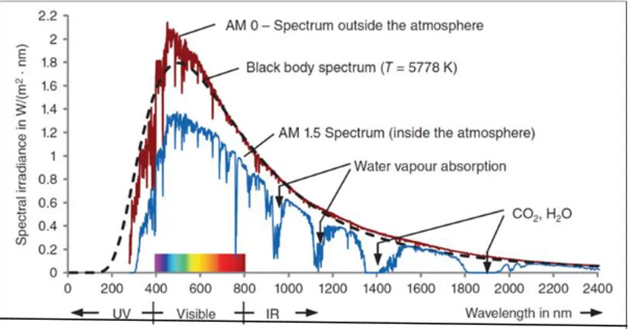
1367 W/M2 is called solar constant which denotes irradiance outside the Earth’s atmosphere. The spectrum outside the Earth’s atmosphere called AM 0 refers to Air mass 0.
Figure 3.1. Spectrum changes when sunlight passes through the atmosphere due to the reflection, absorption, Rayleigh scattering and dust particles (Mertens 2014)
As can be seen at Figure 4.1 spectrum changes when sunlight passes through the atmosphere due to the reflection, absorption, Rayleigh scattering and dust particles. This energy is emitted primarily as electromagnetic radiation in the ultraviolet to infrared and
radio spectral ranges (0.2 to 3 μm). The total mass of the sun is now about 2×1030 kg, and a reasonably stable life with a nearly constant radiative energy output over 10 billion (1010) years is projected (Kwok K et al.2007).
3.4. Fundamentals of Semiconductor Physics
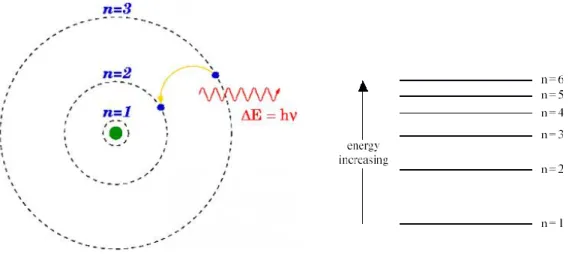
3.4.1 Bohr Model
In atomic physics, the Rutherford–Bohr model or Bohr model presented by Niels Bohr and Ernest Rutherford in 1913, depicts the atom as a small, positively charged nucleus surrounded by electrons that travel in circular orbits around the nucleus-similar in structure to the Solar System, but with attraction provided by electrostatic forces rather than gravity. The Bohr model is a relatively primitive model of the hydrogen atom, compared to the valence shell atom. the Bohr model is still commonly taught to introduce students to important mechanics or energy level diagrams before moving on to the more accurate, but more complex, valence shell atom. According to the Bohr’s second postulate the transfer of an electron from one shell to another occurs under the emission or absorption of electromagnetic radiation. The shells are designated with the letter of K, L, M and so on. Figure 3.2 shows the possible energy states for hydrogen atom.
Figure 3.2. Structure and energy model of hydrogen atom, (Bohr model Wikipedia 20/4/2017)
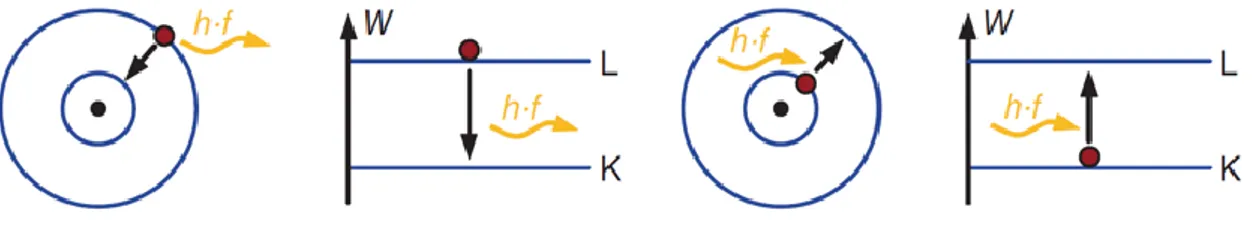
The Bohr model gives almost exact results only for a system where two charged points orbit each other at speeds much less than that of light. This energy is called as ionizing
energy W∞. Figure 4.3 shows the emission and absorption of the light. The frequency of this radiation is determined by the following equation.
∆𝐖 = |𝐖𝟐 − 𝐖𝟏| = 𝐡. 𝐯 = 𝐡.𝐜
𝛌
(3.2)
W1: energy before transfer W2: energy after transfer
h: Planck’s constant = 6.6 · 10-34 W/s
ν: frequency
c: speed of light in a vacuum = 3·108 m/s λ: wavelength
Figure 3.3. Schematic depiction of the emission and absorption of light. (Mertens 2014)
3.4.2 Energy Bands of Semiconductors
Complete energy band diagrams of semiconductors are very complex. However, most have features similar to that of the diamond crystal discussed in section (3.4). In this section, we first take a closer look at the energy band diagrams of common semiconductors. We then present a simple diagram containing only the most important features and discuss the temperature and doping dependence of the energy bandgap. (Bart.Van 2011).
3.4.2.1. Energy Band Diagrams of Common Semiconductors
The energy band diagrams of semiconductors are rather complex. The detailed energy band diagrams of germanium, gallium arsenide and silicon are shown in Figure 3.4. The energy is plotted as a function of the wavenumber, k, along the main crystallographic directions in the crystal, since the band diagram depends on the direction in the crystal. The energy band diagrams contain multiple completely-empty and completely-filled bands. In addition, there are multiple partially-filled band.
3.4.2.2. Simple Energy Band Diagram of a Semiconductor
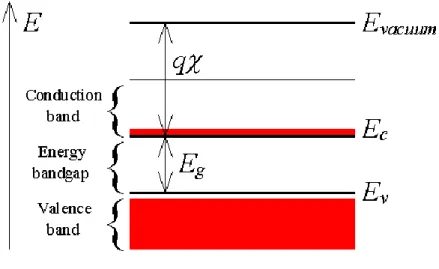
The energy band diagrams shown in the previous section are frequently simplified when analyzing semiconductor devices. Since the electronic properties of a semiconductor are dominated by the highest partially empty band and the lowest partially filled band, it is often sufficient to only consider those bands. This leads to a simplified energy band diagram for semiconductors as shown in Figure (3.4).
Figure 3.4. Simplified energy band diagram for semiconductors.( https://ecee.colorado.edu/~ )
A simplified energy band diagram used to describe semiconductors. Shown are the valence and conduction band as indicated by the valence band edge, Ev, and the
conduction band edge, Ec. The vacuum level, Evacuum, and the electron affinity, χc, are
also indicated on the figure.
3.4.2.3. Temperature and doping dependence of the energy bandgap
This conduct can be understood if one considers that the interatomic spacing increases when the amplitude of the atomic vibrations increases due to the increased thermal energy. This effect is quantified by the linear expansion coefficient of a material. An increased interatomic spacing decreases the average potential seen by the electrons in the material, which in turn reduces the size of the energy bandgap.
High doping densities cause the bandgap to shrink. This effect is explained by the fact that the wave functions of the electrons bound to the impurity atoms start to overlap as the density of the impurities increase.
3.5. Semiconductors
Semiconductor material shows insulator character at absolute zero temperature. But when temperature is increased, it becomes conductor. The typical characteristic of semiconductors is the band gap between conduction band and valence band. At T= 0 K, as conduction band is empty, valence band is full of electrons. To be electrically conductive, charge carriers must move from a state in energy band to another. So under this circumstance, which is that all energy levels are full or empty, conduction cannot happen. When temperature is increased or photon which has higher energy than energy band gap of semiconductor is sent to semiconductor, energy which is needed for passing from valence to conduction band is transferred to electrons. Electron leaving from valence band forms a hole behind. When this hole is filled by another electron, it forms a hole behind too. As a result, there can be seen a hole movement because of the electron which leaves valence band.
3.5.1. n-type Semiconductors
n-type semiconductors have a larger electron concentration than hole concentration. As opposed to p-type semiconductors, the period n-type comes from the negative charge of the electron. In n-type semiconductors, electrons are the majority carriers and holes are the minority carriers. n-type semiconductors are created by doping an intrinsic semiconductor with donor impurities (or doping a p-type semiconductor as done in the making of CMOS chips). A common dopant for type silicon is phosphorus. In an n-type semiconductor, the Fermi level is greater than that of the intrinsic semiconductor and lies closer to the conduction band than the valence band. (Neamen et al. 2003).
3.6. Light Absorption into and Electron Extinction out of a Semiconductor
Light absorption process is widely used for such as Photodetectors, Photodiodes, Photoconductors, Light dependent resistance, phototransistors…etc to activate the conduction mechanism for getting the electrons to move easily. Due to the wave-particle duality principle, light waves could be treated as particles. The energy of a photon is
E = hν (3.3) where h is Plank’s constant and ν is the frequency. We can also relate the wavelength and energy by λ =c ν= hc E = 1.24 E μm (3.4)
Where E is the photon energy in eV and c is the speed of light.
There are several possible photon–semiconductor interaction mechanisms. For example, photons can interact with the semiconductor lattice whereby the photon energy is converted into heat. Photons can also interact with impurity atoms, either donors or acceptors, they can interact with defects within the semiconductor. However, the basic
photon interaction process of greatest interest is the interaction with valence electrons. When a photon collides with a valence electron, enough energy may be imparted to elevate the electron into the conduction band. Such a process generates electron–hole pairs and creates excess carrier concentrations
3.6.1. Photon Absorption Coefficient
When a semiconductor is illuminated with light, the photons may be absorbed or they may propagate through the semiconductor, depending on the photon energy and on the bandgap energy Eg. If the photon energy is less than Eg, the photons are not readily
absorbed. In this case, the light is transmitted through the material and the semiconductor appears to be transparent. If E = hυ>Eg, the photon can interact with a valence electron
and elevate the electron into the conduction band. The valence band contains many electrons and the conduction band contains many empty states, so the probability of this interaction is high when hυ> Eg. This interaction creates an electron in the conduction
band and a hole in the valence band—an electron–hole pair. The basic absorption processes for different values of hυ are shown in Figure 3.5.
Figure 3.5. optically generated electron–hole pair formation in a semiconductor. (Neamen Donald. 2003)
The absorption coefficient in the semiconductor is a very strong function of photon energy and bandgap energy. The absorption coefficient increases very rapidly for hυ> Eg,
or for λ < 1.24/Eg. The absorption, coefficients are very small for hυ>Eg, so the
4.6.2 Electron–Hole Pair Generation Rate
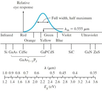
We have shown that photons with energy greater than Eg can be absorbed in a semiconductor, thereby creating electron–hole pairs. The intensity Iυ (x) is in units of
Figure 3.6. Light spectrum versus wavelength and energy. Figure includes relative response of the human eye. (Neamen Donald. 2012)
Energy/cm2-s and αIυ (x) is the rate at which energy is absorbed per unit volume. If we
assume that one absorbed photon at an energy hυ creates one electron–hole pair, then the generation rate of electron–hole pairs is
g = αIυ(x)
hυ
(3.5)
Which is in units of #/cm3-s. We may note that the ratio Iυ (x)/hυ is the photon flux. If, on
the average, one absorbed photon produces less than one electron–hole pair, then must be multiplied by an efficiency factor (Neamen 2012).
3.7. Metal Semiconductor Contacts
3.7.1 Metal–Semiconductor Ohmic Contact
We will start our study of non-homojunctions with the metal-semiconductor contact. This contact plays an important role in almost all junction devices. (Bhattacharya D.K 2007).
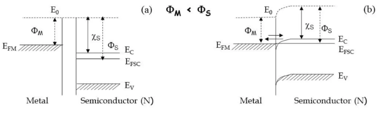
When a metal and an n-type semiconductor are joined and ΦM < ΦS, electrons will flow
from the Fermi energy level in the metal into the semiconductor conduction band to lower their energy. This will cause the chemical potential of the semiconductor to move up into equilibrium with that of the metal. It will also deform the semiconductor bands, so that they curve upwards away from the metal.
Figure 3.7. Metal–Semiconductor – Ohmic Contact
This type of contact yields a linear relationship between the voltage applied and the current that flows across the junction. It is therefore called an ohmic contact, because itobeys ohm's law. This type of contact is also described as metallization, and is used to supply electric current into semiconductor devices.
In contrast, a rectifying contact allows the current to flow for only one voltage regime (negative or positive). The formation of an ohmic contact needs the injection of electrons from the metal to the semiconductor material. As a consequence, the metal work function ϕm has to be lower than the one for the semiconductor material ϕs, as illustrated in figure
3.8 for an n-type semiconductor.
Figure 3.8. Energy band diagram for a metal and an n-type semiconductor, in the case ϕm < ϕs, before contact (a) and after contact (b). (Sze et al. 2007)
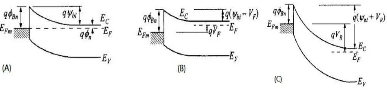
3.7.2. Metal–Semiconductor Rectifying Contact and Solar Cell Operation
To understand semiconductor(M-S) solar cell it is essential to be understood metal-n type semicometal-nductor rectifyimetal-ng cometal-ntact that allow the curremetal-nt ometal-nly ometal-ne way, ametal-nd depletion region wipes the free charges at the junction region.
In terms of M-S contact, It is first necessary to introduce the concept of the work function. The work function of a material is the energy required to remove an electron from the level of the chemical potential and give it enough energy to escape to infinity and arrive there with zero energy. M-S contact displaying asymmetric current-voltage characteristics, i.e. allowing high current to flow across under the forward bias condition and blocking current off under the reverse bias; this behavior is controlled by the bias voltage dependent changes of the potential barrier height in the contact region. (Created et al. 2001-2016).
The parameter is the ideal barrier height of semiconductor contact, the potential barrier seen by electrons in the metal trying to move into the semiconductor. This barrier is known as the schottky barrier and is given, ideally, by
BO = (m – x) (3.6)
On the semiconductor side, Vbi is the built in potential barrier.
Vbi = BO - ∅n (3.7)
Which makes Vbi a slight function of the semiconductor doping.
For the uniformly doped semiconductor, we have
w = xn = [
2∈s(Vbi+VR
eN𝑑 ]
1/2
(3.8)
where VR is the magnitude of the applied revers biased voltage. We can again as
summing an abrupt junction approximation. We will first consider the ideal case without surface states and other anomalies. Figure (3.9) shows the electronic energy relations of a high work-function metal and an n-type semiconductor which are not in contact and are in separate systems. If the two are allowed to connect with each other, for example by an outside wire connection, charge will flow from the semiconductor to the metal and thermal equilibrium is established as a single system. The Fermi levels on both sides will line up. Relative to the Fermi level in the metal, the Fermi level in the semiconductor is lowered by an amount equal to the difference between the two work functions. The work function is the energy difference between the vacuum level and the Fermi level.
Figure 3.9. Energy band diagrams of metal semiconductor contacts. Metal and semiconductor (a) in separated systems, and (b) connected into one system. As the gap S(c) is reduced and (d) becomes zero. (Sze,et al. 2007)
When this relationship is established, it serves as a boundary condition to the solution of the Poisson equation in the semiconductor, which proceeds in exactly the same method as in a p-n junction. The energy band diagrams for metals on n-type material are shown, under different biasing conditions, in Figure (3.10).
Solar power systems like the one on our roof, produce power directly from the sun. Sunlight is converted directly into electricity by each solar cell in the panels. There are many factors which affect how well the cells do that. The solar cells are made of silicon that has been combined with other materials in such a way that there are extra electrons in one part of the cell, and missing electrons in another part of the cell. When the sunlight strikes the cell, photons in the light knock some of the extra electrons loose from the
Figure 3.10. Energy-band diagrams of metal on n-type semiconductors under different biasing conditions. (a) Thermal equilibrium. (b) Forward bias. (c) Reverse bias.
silicon, and they flow to the part of the cell that is missing electrons. This flow produces an electrical current that eventually reaches the inverter, where it gets converted into usable electricity.
The title that explains what the “Current status” numbers mean, goes into more detail about the way the electrical current works and what the inverter does. Regular solar cells, like the ones on our roof, can only convert around 15% of the sunlight that strikes them into electricity. They are still a new and developing technology (modern solar cells were only invented in 1954). The theoretical limit for regular cells is 30%. More advanced solar cells can reach higher conversion rates, over 60% in theory (Sze et al. 2007).
Figure 3.11. Solar cells with resistive load (Sze et al. 2007)
Consider the solar cells with a resistive load. Even with zero bias applied to the junction, an electric field exists in the space charge region. Incident photon illumination can create electron–hole pairs in the space charge region that will be swept out producing the photocurrent IL in the reverse-biased direction as shown. The photocurrent IL produces a
voltage drop across the resistive load which forward biases the solar cells. The forward-bias voltage produces a forward-forward-bias current IF. The net solar cells current, in the
reverse-biased direction is;
I = IL− IF = IL− IS[exp (eV
Where, Is is defined by,
Is = A. A∗T2exp (−eBn
kT ) (3.10)
The ideal diode equation has been used. As the diode becomes forward biased, the magnitude of the electric field in the space charge region decreases, but does not go to zero or change direction. The photocurrent is always in the reverse-biased direction and the net solar cell current is also always in the reverse-biased direction. There are two limiting cases of interest. The short-circuit condition occurs when R = 0 so that V = 0. The current in this case is referred to as the short-circuit current, or
I = Isc = IL (3.11)
The second limiting case is the open-circuit condition and occurs when R → ∞. The net current is zero and the voltage produced is the open-circuit voltage. The photocurrent is just balanced by the forward-biased junction current, so we have
I = 0 = IL – IS[exp ( eVoc kT ) − 1] (3.12) to extract Voc IL / IS =[exp ( eVoc kT ) − 1] (3.13) ln(IL / IS+1) =eVoc kT (3.14) Voc = kT eln (1 + IL Is) (3.15)
where kT/e is thermal potential (Vt) so, we can rewrite the equation as;
Voc = Vt ln (1 + IL
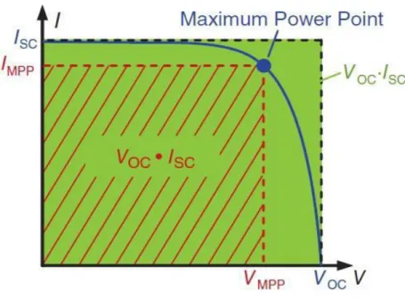
Figure 3.12. Forward bias I-V curve in illuminated conditions showing PV cell parameters
The conversion efficiency of a solar cell is defined as the ratio of output electrical power to incident optical power. For the maximum power output, we can write
η = Pm
Pin× 100% =
Im . Vm
Pin × 100%
(3.17)
The maximum possible voltage and the maximum possible current in the solar cell are Voc and Isc, respectively. The ratio ImVm/IscVoc is called the fill factor and is a measure of
the realizable power from a solar cell.
FF =V m . I m
Voc . Isc=
Pm
Voc . Isc
Gold is a very precious metal and a chemical element that has the symbol Au and atomic number 79 in the periodic table. Aluminum (Al) is the most abundant metal and the third most abundant element in the Earth. It is nonmagnetic, soft, ductile metal. Atomic number is 13. Silicon is extremely important for photovoltaic devices. It has the atomic number 14 and situated in the fourth main group. Silicon wafer also known as substrates is a thin slice of semiconductor material used in electronics, integrated circuits, photovoltaic for solar cells. Methylene blue (or MB) is a basic aniline dye with the molecular formula C16H18N3SCl. At room temperature, it appears as a solid, odorless,
dark green powder that yields a blue solution when dissolved in water. It has many uses in a number of different fields. For instance, chemists use it to detect oxidizing agents and biologists use it to stain tissue samples and detect nucleic acids. In medicine, it is used as a treatment for various illnesses and disorders, including methemoglobinemia, schizophrenia, kidney stones, and herpes infections. In aquaculture, it is used to prevent freshwater fish eggs from being infected by bacteria and fungi. Molybdenum chemical element in the periodic table. His character is Mo and atomic number 42. (Wikipedia 14/5/2016).
Figure 4.1. The Mo/Methylene Blue/n-Si/ Al/Au contacts structure
The researchers of the study and the results obtained during the shortcomings of the expenses related to the subject they study the achievements, innovations and the benefits brought to the forefront, to be considered for publication constitutes the scope of this process. In this study, we have used n-Si crystal with [100] direction, grown as bulk, and has 12-16 Ω-cm resistivity. The aim of this study showing the effect the organic components (methylene blue) on the electrical characteristics of the diodes. For this purpose, we have Mo/Methylene Blue/n-Si/ Al/Au diodes, and using different annealing temperature.
Figure 4.2. UV-Vis spectrum of methylene blue solution, with maximum absorption at 668 nm
In this experiment, the samples those fabricated at this work are 2 group; one included the samples that is not annealed (as deposited) and the other group is annealed at 400 0C. Every group of samples are fabricated by three different thicknesses of rectifying contact (Mo); 10 nm, 20 nm and, 30 nm. The samples are named as; A1, A2, A3, A4 and A5. A1 is named for the reference sample, A2 is named for the sample that the surface of Si wafer is swam in 10%HF then the interface material is spinned. A3 is named for the sample that the surface of Si wafer is swam in 10%HCl then the interface material is spinned. A4 is named for the sample that the surface of Si wafer is swam in 10%HF then
the interface material is coated by dropping. A5 is named for the sample that the surface 0of Si wafer is swam in 10%HCl then the interface material is coated by dropping.
The study on the Si wafer will be done firstly get have 1014 to 1018 with carrier density n-type. Later cleaning Si wafer procedure by the ultrasonic washed in the acetone next methanol for 10 minutes. Later washed in deionized water. Next washed RCA1 (H2O:H2O2:NH3;6:1:1) at 60 oC for 10 minutes. Washed in diluted HF (H2O;HF;10:1) for
30 seconds. Later to boil in RCA2 (H2O:H2O2:HCl;6:1:1) at 60 oC for 10 min. later
thoroughly washed by deionized water. Washed in diluted HF (H2O;HF;10:1) for 30
seconds. Subsequently 15-20 min will be in deionized water subsequently dried with N2
pressurized inert gas. Made ohmic contacts to the matte side of the sample. Later heating washed with 10% HCl, washed with deionized water and dry thoroughly. Then be ready to replace burned placed inside the vacuum device. Then in 99.98% purity aluminium (Al) to be evaporated, ohmic contact metal to be placed on the heater and chemically cleaned to do thermal cleaning process with pre-melting process. Just after we receive the mat side of the heater that will be placed facing the sub-systems and evacuation procedures is initiated. After allowing to drop to ~ 10-7 bar pressure by ohmic contact
evaporation metal source and is coated on whether the current heater pad (~ 100nm in thickness) will be provided. Meanwhile thickness of the material that is coated will be detected by quartz sensor. To prevent (Al) oxidation to be covered on a thin layer of gold (Au) without breaking the vacuum of the chamber. After waiting a while to be given air into the vacuum device and subtracting the sample, the sample into the furnace set to 585 °C in chemically cleaned a quartz crucible for 3 minutes to anneal. So that the ohmic contact process is completed. This wafer will be divided into two parts. As reference (without interface) and, inorganic matter Methyl Blue. Solvent mixed will get ready. The one part ohmic contact Si is vacuumed on the chuck and spinned at a certain speed in order to organic and organic/inorganic solution to be coated. Then the wafer that is coated annealed at 100-200 °C.
Figure 4.3. The methylene blue, chemical structure and molecules (Lab on a Chip Issue 6. 2010)
Then to make of the rectifying contacts process both wafers that is coated or uncoated prepared for Al sputter NVTS 400 supports devices to be placed and covered with 5 mm in diameter and 10-50 nm thick Al layers will undergo a light. Later in the 100 nm thickness of 1 mm diameter Al layer for receiving an edge of the contact it will be covered by the evaporation method. Then a time to cool the pad, wait air be given for system, and will be issued holders. Prepared Mo/n-Si/Organic, reference/Al/Au to do measurements whether the probe station system, Keithley’s 2400 and COINC-16S-150-002 Solar Simulator and lab view on a control program written in by Asst. Prof. Dr. Kadir EJDERHA help the characterization of these cells will be made in different sunlight power.
4.1. DC Magnetron (Sputtering) Method
Ignition studies, in the semiconductor surface to coat the sputtering method is widely used. This method results in positive ion bombardment of heavy usually on a removable base of a portion of atoms in an electrode used as the cathode is based on forming a thin layer. Sputtering method can be performed basically in three different ways. These DC (Direct Current, DC), RF (Radio Frequency) and DC-RF sputtering techniques. Each of these three methods can be made more effective with the help of magnetic fields.
Figure 4.4. The Magnetic Field DC Sputtering (Sputtering) Method, (R.S. Pessoa et al. 2014)
Magnetic field in DC sputtering, under a magnetron positioned target metal electrical field through the directed ions solenoidal magnetic-field (coil spring), movement target metal shock and the growth incident on the material base to which it breaks of some of the atoms. DC sputtering method in a magnetic field about 100 m Torr pressure with argon gas atmosphere by means of the electric field applied to the magnetic field approximately perpendicular. Ar plasma (ionized atoms completely cloud) is created. Then the current through the electric field and ions of the plasma electrons (-e) begins to accelerate in the opposite direction. Ar atom is given a positive valence for e and Ar + ions for negative voltage is applied to the metal target will begin accelerating towards the target. Ions entering the magnetic field with this speed; the effect of the magnetic field source is from the inside out in a magnetic field will begin to move in a circular orbit. This force creates movement;
It can be expressed. Here; q charge of the ion, the speed of the ions, B magnetic field and F formed on the Ar + ion is a force perpendicular to the magnetic field and the velocity of the ions. The rotary motion by the effect of this force will make the movement target metal ion-correct a displacement due to the electric field. Thus solenoid Ar + ions will hit a moving target metal. This target metal atoms will break on impact. This shock and scattered due to the vomiting (which is the name of this process here), these atoms will spread rapidly. This will extend over a portion of the substrate and atoms emitted from a thin metal film on the base material will grow. This process is referred to as thin film deposition method by DC sputtering in a magnetic field (Ejderha 2012).
4.2 Rotation (spinning) Film Coating Technique
Rotating basically consists of four phase’s thin film coating event. The first stage placing the solution on the surface to be coated (deposition). The second stage Quick rotation (spin-up). The third stage stopping the rotation (spin-off). The fourth stage Evaporation (evaporation) is composed of Step.
Figure 4.5. Rotation (spinning) Film Coating Technique (2015 Elveflow)
The first step in the solution is excessive amount relative to the film thickness when the coating placed on the surface. The second stage, with this excess speed rotation due to effects such as viscosity and rotation speed of the liquid surface of the solution to be coated are dispersed outwardly. Constant angular speed of rotation is provided at the desired time in the third stage. At this stage, no longer homogeneous thin film formation
takes place. Evaporation heat treatment which is the last part, when substrates subjected to heat treatment, other materials having lower vaporization temperature than the evaporation temperature of the desired material to be coated are removed from the medium (Gördün, 2011). Results will only be obtained from the surface of a film coated with the desired material.
4.3. Annealing Furnace
Annealing, in metallurgy and materials science, is a heat treatment that alters the physical and sometimes chemical properties of a material to increase its ductility and reduce its hardness, making it more workable. It includes heating a material to above its recrystallization temperature, maintaining a suitable temperature, and then cooling. In hardening, atoms travel in the crystal lattice and the number of dislocations decreases, leading to the change in ductility and hardness. In the cases of silver, copper, steel, and brass, this process is performed by heating the material (generally until glowing) for a while and then slowly letting it cool to room temperature in still air. Silver, Copper, and brass can be cooled slowly in air, or quickly by quenching in water, unlike ferrous metals, such as steel, which must be cooled slowly to anneal (Lucas-Milhaupt, 2011-2017).
Figure 4.6. The Annealing Furnace system
4.4. Characterization Procedure
It will be noticed that the curve produced under illumination is simply shifted from the other curve by a value of Isc, which represents the constant generation of current by light.
This value is called short-circut current, because it is a current generated under the light at zero voltage. The value of Voc, in contrary, open-circuit voltage, voltage under
Figure 4.7. Characterization procedure.
The operating point, at which the maximum power is provided is called the Maximum Power Point (MPP). As the power of a working point always corresponds to the surface of I·V, this area must be maximum in the case of MPP. The fill factor (FF) describes the relationship of MPP and the product from open-circuit voltage and short-circuit current. As can be seen at figure, FF shows the size of the area under the MPP working, compared to the area Voc·Isc.
Figure 4.8. Current–voltage characteristics of n-type solar cells with 10 nm at room temperature with different method in the light and dark
I started make and prepared fife simple I called A1, A2, A3, A4, A5, and collared lines. Each of them is separated from the others. Presentation On the front page. After meshared all simple I see different result but The results are not very perfect. In Figure (4.8) that the specimens are sensitive to the effects of light and darkness.
-2 0 2 Voltage (V) 10-10 10-9 10-8 10-7 10-6 10-5 10-4 10-3 10-2 CU RR EN T (I ) - - - Light ___ Dark 10 nM at Room tem Sample Pm ff n A1 1.598.10-6 0.247 %8.138.10-3 A2 1.091.10-6 0.241 %5.555.10-3 A3 8.393.10-7 0.251 %4.274.10-3 A5 1.34.10-7 0.221 %6.826.10-6
Figure 4.9. Current–voltage characteristics of n-type solar cells with 10nm at 400 0C temperature with different method in the light and dark
Results of previous experiments are not good, I think and I decided annealed of simples at 400 OC, I noticed that the results were changed better than they were in the Fieger
(4.9), Again the samples called the same A1, A2, A3, A4, A5 and used the same colors.
-3 -2 -1 0 1 2 3 Voltage (V) 10-12 10-11 10-10 10-9 10-8 10-7 10-6 10-5 10-4 10-3 C U R R E N T ( A ) - - - Light ___ Dark 10 nM at 400 oC Sample Pm ff n A1 3.183.10-10 0.301 1.621.10-6 A2 6.114.10-10 0.124 3.114.10-6 A3 5.066.10-10 0.282 2.58.10-6 A4 1.45456.10-9 0.262 1.34.10-13 A5 4.00069.10-8 0.219 7.83.10-12
Table 4.1 The Pm, FF and, of 10 nm samples for as-deposited and annealed at 400 0Cof Mo/MB/n-Si/Al/Au solar cells
10 nm at as-deposited 10 nm at 400 0C Sample Pm FF Pm FF A1 1.598.10-6 0.247 %8.138.10-3 3.183.10-10 0.301 %1.621.10-6 A2 1.091.10-6 0.241 %5.555.10-3 6.114.10-10 0.124 %3.114.10-6 A3 8.393.10-7 0.251 %4.274.10-3 5.066.10-10 0.282 %2.58.10-6 A4 1.45456.10-9 0.262 %1.34.10-13 A5 1.34.10-7 0.221 %6.826.10-6 4.00069.10-8 0.219 %7.83.10-12