DEVELOPMENT OF A WIRELESS MULTICHANNEL
NEURAL DATA TRANSMISSION SYSTEM
A THESIS SUBMITTED TO
THE GRADUATE SCHOOL OF
ENGINEERING AND NATURAL SCIENCES
OF ISTANBUL MEDIPOL UNIVERSITY
IN PARTIAL FULFILLMENT OF THE REQUIREMENTS FOR
THE DEGREE OF
MASTER OF SCIENCE
IN
ELECTRICAL, ELECTRONICS ENGINEERING AND CYBER SYSTEMS
By
Muhammad Rizwan Mukati
September, 2017
iv
ABSTRACT
DEVELOPMENT OF A WIRELESS MULTICHANNEL
NEURAL DATA TRANSMISSION SYSTEM
Muhammad Rizwan Mukati
M.S. in Electrical, Electronics Engineering and Cyber Systems Advisor: Assist. Prof. Tuncer Baykas
September, 2017
Implantable microelectrode arrays enable multichannel electrophysiological recordings from the mammalian brain during behavioral experiments. Wireless data transmission systems combined with the microelectrode arrays and electrophysiology hardware allow the chronically-implanted subjects to freely move during the neural recording sessions. In the present study, a wireless neural data recording system is designed and implemented to collect data from behaving rats. The system is based on an amplifier chip and a microcontroller with 802.11 technology at the client side, and a PC equipped with LabVIEW software at the server side. The system enables data throughput up to 6.4 Mbps for signals obtained from 16 channel microelectrode arrays with a sampling rate of 25 KHz per channel. Based on five recording sessions each lasting 12.8 seconds, 9927.6 UDP packets ± 105.85out of 10000 packets each consisting of 1024 bytes were received and recorded by the server. The present system offers a cost-effective and compact solution to perform multichannel in vivo electrophysiological recordings from behaving rats. We also provide the design and 3D models of silicon-based micro-machined microelectrode arrays for extracellular neural signals from 8-32 channels and evaluate the mechanical strength of these probes using simulations.
v
ÖZET
KABLOSUZ ÇOK KANALLI SİNİRSEL VERİ İLETİM
SİSTEMİNİN GELİŞTİRİLMESİ
Muhammad Rizwan Mukati
Elektrik-Elektronik Mühendisliği ve Siber Sistemler, Yüksek Lisans Tez Danışmanı:Yrd. Doç. Dr. Tunçer Baykaş
Eylül, 2017
Bu çalışmada, uyanık sıçanların sinirsel aksiyon-potansiyelinin iletilmesi için kompakt boyutlu kablosuz bir verici sistemi tasarlanıp, üretilmiştir. IEEE 802.11 teknolojisini kullanan sistem 16 ayrı mikro elektrottan alınan veriyi 6.4 Mbps hızında yollayabilmektedir. Deney hayvanlarına dolaşma imkanı veren bu sistem onların stres seviyesini düşürerek daha başarılı ölçümleri mümkün kılmaktadır.
Ayrıca, çalışmanın ikinci kısmında silikon tabanlı mikro-işlenmiş mikroelektrotların tasarımı açıklanmıştır. Yani tasarımlar sinirlerden 32 kanala kadar sinyallerin düşük gürültü ile alınmasına imkan vermektedir.
vi
Acknowledgement
I would first like to express my sincere gratitude to my supervisor Dr. Tuncer Baykas for continuous support of my master research or thesis writing and for keep providing motivation. Furthermore, I would like to thank Dr. Mehmet Kocaturk for introducing me to this topic and guiding me throughout this degree. Without his passionate participation and input, this work could not have been successfully conducted. I am very thankful to him for always being so helpful and encouraging.
Last but not the least, I would like to thank to my family for providing me support and continuous encouragement throughout the entire process. This accomplishment would not have been possible without them.
vii
Contents
1 Introduction ... 1 1.1 Aim ... 1 1.2 System Requirements ... 2 1.3 System Structure ... 2 2 Literature Review ... 42.1 Wireless Neural Recording Systems ... 4
2.2 Microelectrode Arrays ... 9
Microwire arrays ... 9
Micromachined arrays ... 11
3 Main Parts of the Recording System ... 14
3.1 Analogue Front End for Data Acquisition ... 14
Characteristics of Analog front end (AFE) ... 14
Front end chip used in the experiments ... 16
Serial Peripheral Interface ... 18
3.2 Data transfer ... 21
Network Protocols ... 21
Wi-Fi and 802.11 Standards ... 24
3.3 Comparison of the Wi-Fi modules ... 26
viii
NodeMCU ... 27
Particle Photon ... 28
ESP- WROOM-32 ... 28
4 System Realization... 30
4.1 Microelectrode Array (MEA) Development ... 31
4.2 Recording System Development ... 40
5 Experimental Results ... 50
5.1 Preliminary Results ... 50
5.2 Results from the Experiment on a Test Animal ... 51
6 Conclusions and Future Work ... 59
Bibliography ... 60
ix
List of Figures
1-1: Structure of the overall system. ... 3
2-1: Implantable Microwires. (a) Microwire arrays connected with the Omnetics connector. (b) High-density microwire arrays ... 10
2-2: Basic structure of silicon based Michigan probe. ... 11
2-3: Utah silicon-based 100 microelecrode electrode array, (a) Utah flat electrode array, (b) Utah slanted electrode array ... 12
2-4: Silicon on Insulator (SOI) wafer ... 13
3-1: Schematic diagram of RHD2132 chip... 18
3-2: Cascading several SPI devices. ... 19
3-3: Master with independent slaves ... 20
3-4: Block diagram of ESP32 SoC ... 29
4-1: System architecture of Wireless Neural Recording System. ... 31
4-2: 3D view of the probe. ... 33
4-3: Front view of the probe. ... 33
x
4-5: Stress curves, the first plot shows the varying stress values while changing probe width (um) and keeping probe thickness constant. The second plot shows the varying stress values
by varying the probe thickness and keeping probe width constant. ... 34
4-6: Stress values with varying probe thickness of different length of the probe. ... 35
4-7: Mask of all 24 designs of microelectrode array. ... 36
4-8: Design of microelectrode array ... 37
4-9: All 8 shanks of single microelectrode array ... 37
4-10: Closer view of the individual shank out of 8 shanks, arrangement of electrodes on shanks and tip width. ... 38
4-11: Recording pads and traces that connects that connects with the electrode ... 38
4-12: Block diagram of Wi-Fi module, CMOS-LVDS converter and Amplifier board... 41
4-13: Internal logic diagram of SN65LVDT41 ... 42
4-14: Connection diagram of (ESP-32 board, SN65LVDT41 and RHD2132 Amplifier board). ... 42
4-15: Block diagram of UDP server that counts the total number bytes and packets received and writes data on TDMS file. ... 46
4-16: Block diagram that converts TDMS file to CSV file. ... 47
4-17: Front panel of the program that convert TDMS file to CSV format ... 47
4-18: Code written in MATLAB for converting bytes in to values and sorting data according to their Channels. ... 48
4-19: Block diagram of 16-channel UDP server with data-logging. ... 48
xi
5-1: 10000 packets (10MB of data) captured in Wireshark. ... 52
5-2: Histogram plot of the captured packets in equally size time interval ... 52
5-3: Front panel of UDP server that counts the total number bytes and packets received and writes data on TDMS file... 53
5-4: Plot for 1st four channels on MATLAB. ... 53
5-5: Microwire array implanted in the rat brain and RHD2132 amplifier Chip. ... 54
5-6: CMOS-LVDS converter connected with the module using 802.11n technology ... 54
5-7: Recorded Neural signal from channel 7 ... 55
5-8: Histogram of 1st trail... 56
5-9: Histogram of 2nd trail. ... 56
5-10: Histogram of 3rd trail. ... 57
5-11: Histogram of 4th trail. ... 57
5-12: Histogram of 5th trail. ... 58
5-13 : Distribution of packet arrival intervals. ... 58
A.1 : GUI(Graphical User Interface) of Hercules ... 69
A.2 : Second trial 10000 packets (10MB of data) captured in Wireshark. ... 69
A.3 : Third trial 10000 packets (10MB of data) captured in Wireshark. ... 70
xii
List of Tables
1.1: Required data rate of different sampling rate and channels. ... 2
3.1: Comparison of TCP and UDP. ... 23
4.1: Parameters of MEA designs. ... 39
4.2: ADC sampling rate ... 41
4.3: Connection pins of RHD2132 Amplifier board (AFE), CMOS-LVDS converter and ESP-32 board (MCU + Wi-Fi module) ... 43
4.4: Command for performing analog-to-digital conversion ... 43
4.5: Result sent back by RHD2132 to module... 43
A. 1: Values for variable in Register 8-11 for setting upper bandwidth of the amplifier ... 67
A. 2: Values for variable in Register 8-11 for setting lower bandwidth of the amplifier ... 68
1
Chapter 1
1 Introduction
Chronically implantable microelectrode arrays enable multichannel electrophysiological recordings from the mammalian brains during behavioral experiments [1] [2]. Wireless data transmission systems combined with the microelectrode arrays and electrophysiology hardware allow the subjects to freely move during the neural recording sessions [5].
In this work, we are focusing on two aspects such a recording system design. First, we develop a wireless data acquisition part, which provides required data throughput for a 16 channel array. Second, we design the microelectrode array, which enable such recordings.
1.1 Aim
Our aim is to provide low cost, compact size multichannel wireless neural data transmission system that can provide high data rate. In addition, to create designs of silicon based microelectrode arrays to penetrate easily to the brain tissue without damaging neurons and provide high selectivity, low impedance and high SNR. In this thesis, we have developed a prototype for the in vivo recording from the motor cortex of the rat which can record signals
2
from 16-channels and can sample each channel at 25 KHz and capable of wireless transmission of data.
1.2 System Requirements
A system can be capable of recording signals from 16 channel and measure 25000 samples per second (SPS) from each channel with a 16-bit of resolution and transmit the data wirelessly to the server which can display and store the data for further analysis. Table (1.1) shows the required data rate for different sampling rate and number of channels.
25 kilo samples per second per channel.
16 channel recording.
16-bit of resolution.
Action potential.
Required data rate is 6.4 Mbps.
Data logging.
Table 1.1: Required data rate of different sampling rate and channels.
1.3 System Structure
The structure of the overall system is shown in Figure (1.1) that represents the flow of the signal. The first step is to acquire the signal from the rat brain using microelectrode array.
3
Afterwards, amplification, sampling and quantization is performed to convert the signal from analog domain to digital domain using the digital electrophysiology interface chip. The Wi-Fi module using 802.11n technology takes that signal, process and transmit it to PC which displays and saves the data.
4
Chapter 2
2 Literature Review
2.1 Wireless Neural Recording Systems
In the literature, many wireless recording systems can be found, which are developed for different requirements. In [7], a system developed that transmit data into the body wirelessly by modulating a signal using frequency-shift keying and recording signal and transmitting out of the body from multiple channels on the implanted device. Where “Each channel is designed to support reverse telemetry”[7] with up to data rate of 3Mbps and recording neural signal from 16 channels. Furthermore, according to design developed by which it can be possible to power up the system wirelessly.
In [8], a system for wireless neural recording is developed of 32 channels uses time-division multiplexing and can be powered up inductively which eliminates the need of a battery thus can be used for long term recording . According to the authors: “Closed-loop inductive power control with optimal coil designs provides high-power transfer efficiency and maintains the received power at the head stage despite animal movements”[8]. This system reduces power consumption by reducing the amount of current in low noise amplifiers. Animals do not need to carry bulky batteries during the recording sessions. PWM/FSK/OOK modulation options are avalilable and the data rate of this system is between 58 to 709 KSPS. Data carrier frequency options are 433 MHz and 915 MHz.
5
In the article entitled, “Wireless Neural Recording With Single Low-Power Integrated Circuit”, authors designed and fabricated a neural recording chip which contains amplifiers, analog to digital converter (ADC) with a 10-bit of resolution, and threshold based spike detectors and frequency-shift keying transmitter, to record data from monkey brains [9]. The ADC can sample the signals at 15.7 KSPS from 100 channels. An inductive coil is used for providing clock, command signals and power. Transmission of data is accomplished by radio-frequency (RF) telemetry. “The chip requires only two off-chip components: a coil to receive the power and command signals inductively, and a single off-chip 100-nF capacitor to assist in power supply regulation” [9].
In “An Implantable 64-Channel Wireless Microsystem for Single-Unit Neural Recording”, recording the neural signals from the motor cortex of a monkey is accomplished by an implantable microsystems which employs a 64-channel array [10]. The system comprises of signal pre-conditioning module, neural processing unit and a bi-directional telemetry chip that contains both forward and reverse telemetry. The spike occurrences is determined and transmitted after the amplification of the signal by 60 dB. OOK modulation with Manchester coding is used for transmission. The received signal on the receiving end are first amplified and demodulate by OOK demodulator and then in order to retrieve the signal back, Manchester decoding is performed. In vivo and in vitro experiments were performed in that study.
In [11], a 10×10 Microelectrode array integrated with a mixed signal chip is developed and fabricated. The system receives power inductively from an ac coil of 6mm, which is mounted on the chip. It is further rectified and regulated to provide 3.3V DC power supply. Flip chip bonding is done with the Microelectrode array. Neural signals are collected from the electrodes, which are amplified with a 60dB gain. The signal are digitized and transmitted serially over the RF link using an FSK transmitter. During the experiments, 88 electrodes are used for recording and the remaining ones are used for stimulation. Recorded channels are sampled at 15 KSPS, as a result, the data rate of 10.56 Mbps is required which is above the
6
throughput of the system. Therefore spike detection is performed during which user can control the threshold level.
Another system, which is developed for recording EEG signals, is explained in “A TinyOS-Enabled MICA2-Based Wireless Neural Interface”[12]. The system employs a wireless smart sensor modules known as MICA2 and MICA2dot which contain built-in ADC and capable of providing wireless communication (commercially available from Crossbow Technology Inc.[13]). The data rate is 9.6 Kbps. MICA2 on the receiver side receives the signal and sends it serially to PC. Authors have improved the throughput of the module by developing a new MAC protocol “that instructs the transmitter to send whenever the radio-transmit buffer is full” [12].
In [14], an integrated circuit is fabricated using 1.5um CMOS process which consist of 8-channel preamplifier, 8:1 analog multiplexer and digital block which contain ring counter which generates the three bit control signals for the eight channel multiplexer “that sequentially samples each data channel during one sampling window” [14] and the system transmits neural data wirelessly using analog FM.
Incorporating Wi-Fi technology to transmit neural signal wirelessly is presented in “A wearable wireless system for olfactory (of or relating to the sense of smell) neural recording in freely moving rats based on Wi-Fi technology” [15]. Authors developed a system, which comprises of 8-channel micro-wire microelectrode array for recording neural signals up to 50uV-1mV. Signals are amplified on head stage by 13dB using TLC2274 after that they are filtered and amplified by 17dB on backpack using TLC2264 then the signal digitized by an internal analog to digital converter with 12-bit of resolution at a sampling rate of 15 KSPS for each channel. This module consist of STM32F205 chip, which operates at a clock speed of 120MHz, integrated with the Wi-Fi chip BCM43362. After digitizing the signal, it is transmitted wirelessly using Transmission Control Protocol (TCP) [15].
7
Wireless implantable system of 32-channel developed in [16], can record local field potential signals and can detect spikes from neurons and can provide current stimulation with different frequency and amplitude to neurons. Rechargeable battery is used to power up the whole system and that can charge by “novel ultrasonic wireless power delivery module” [16]. The chip that is used in this system is specifically designed to record electrophysiological signals. The chip contains amplifiers for multiple channels, which provide a fixed gain. Bandwidth of the amplifiers are programmable to record different types of brain signals. The chip contains 16-bit ADC and a SPI interface. Within the same system “Bluetooth low energy and 2.4GHz proprietary SoC” [17] communication module is interfaced with the AFE (analog front end). This module support µESB protocol, which is used to obtain more throughput due to which spike detection is possible. All 32 channels sampled at 3 KSPS. On the receiver end a dongle is programmed to receive data over the wireless link [16].
In [18], a custom designed front-end IC is produced for bio-potential signal amplification with adjustable gain and bandwidth and it is integrated with the “commercial off-the-shelf (COTS) FM IC”[18]. Transmitted signals are demodulated using FM demodulator on the receiver board, which are then filtered and amplified and fed to a PC.
A custom bio amplifier circuit of 80-dB gain is designed and fabricated by CMOS process to integrate with the system for wireless neural recording application in “Wireless, In Vivo Neural Recording using a Custom Integrated Bioamplifier and the Pico System” [19]. System is divided in to transmitter and receiver parts. Transmitting side consists of custom amplifier, MSP430 Microprocessors and the RF transmitter. The microprocessor MSP430F1611 used in this work has internal analog-to-digital (A/D) converter of 12-bit of resolution with eight analog input channels. The transceiver nRF2401 used in this work has a capability to provide data rates up to 250 Kbps. Recordings of spike potentials from a live subject are performed. A/D converter digitizes signals with each channel sampled at 20 KHz and signal is transferred to the wireless module for wireless transmission. On the receiving end, signals are relayed to MSP430 processor for formatting and passed through to the CP2103 USB bridge to software running on a PC [19].
8
Using the Bluetooth technology to transmit the firings recorded from an individual neuron of a rat is described in “A wireless recording system that utilizes Bluetooth technology to transmit neural activity in freely moving animals” [20]. This system comprises of headstage and backpack. The headstage consists of an amplifier and filter. The backpack comprises of multiplexer, decoder, amplifier and dsPIC30F6010 which is interfaced with the “Bluetooth v2.0 transceiver”[20]. Recording is performed by using hippocampal array electrode of 16 channel which is then amplified by 20 dB and band pass filtered 250Hz to 6.0kHz using “T16G100 headstage (top center TBSI Inc.)”[20]. Signals from 16 channels are multiplexed using two dual ADG709 decoders. These 4-channel signals are amplified 16 dB prior to the input to A/D converter in microcontroller and then each channel sampled at 25 KHz with a 10-bit of resolution and spike-thresholding is performed. On the receiving end “Host interface uses commercial-off-the-shelf Bluetooth v2.0 transceivers plugged into the USB interface of either desktop or laptop computer” [20].
Authors explain the fabrication of a custom chip for the amplification of neural signals in “An Embedded System Architecture for Wireless Neural Recording” [21]. The chip is integrated with the commercial of the shelf module TelosB mote comprised of 8 MHz TI MSP430 microcontroller, an IEEE 802.15.4, 250 kbps, high data rate radio [22]. Two modes of operation has been performed, which are the real-time neural-signal compression mode and absolute-threshold-based spike detection mode [21]. Single channel is sampled at 4 KHz with a 12-bit of resolution for a real time mode. For spike detection mode the sampling rate is 16.7 KHz with a 12-bit of resolution. The signal is send to the server, which can retrieve the signal. “The client application also enables the user to set amplifier gain and high-pass corner frequency remotely” [21]. The power consumption for the real-time mode is 50mW. In spike detection mode the power composition is between 1-5mW.
All of the mentioned systems have either a limited number of recording channels or insufficient sampling rates for the detection and sorting of the neural spikes for our application. Thus, we designed our own system in this work.
9
2.2 Microelectrode Arrays
In neural recording systems, electrodes must be able to record the signals from neurons for a longer period with the stable brain tissue connection. In addition, electrodes should have the capability of stimulating neurons. For high charge transfer, electrodes must also have a low impedance and high spatial resolution. But, if manufacturers decrease the electrode size to obtain higher spatial selectivity then impedance gets higher which results in low SNR [3].
In order to overcome these issues, different approaches and techniques for fabrication can be applied with different material and geometry [3]. In this work, two main types of microelectrode arrays (MEAs) are reviewed: Microwire arrays and Micromachined arrays.
Microwire arrays
Microwire electrodes are the first implantable electrodes and produced from the very fine metal wires. Accessing deep brain structures is possible by using microwires and recording from a single and specific neuron is possible using these microwires as illustrated in Figure (2.1). Main drawback of such systems are wire deformation during implementation. Furthermore, electrodes have compatibility issues with electronic circuits [3]. In addition, manually assembling of each probe in to an array with exact spacing among each other is difficult to achieve [2].
Different materials are used to fabricate the microwire electrode arrays such as gold (Au), platinum (pt), stainless steel, tungsten (W), iridium (Ir). The tips of the stainless steel electrodes are more delicate so tungsten is more preferable because of its rigid and rough structure for a stable recording. However, recording of low frequency signals using tungsten is harder due to high noise floor. Platinum electrodes allow stable recording along with high signal to noise ratios and impedance of this structure is lower. Main disadvantage is that platinum is mechanically frail [3]. Iridium metal wires are highly stiff and provide more
10
resistance to corrosion and can yield to boost the maximum charge density because of the electrochemically activated surface [23][3].
Figure 2-1: Implantable Microwires. (a) Microwire arrays connected with the Omnetics connector. (b) High-density microwire arrays [23] [3].
In order to improve the performance of the microwires for recording and stimulation, carbon nanotubes and conductive polymers are used for coating the tip of the electrode. An experiment was conducted by the group of researchers in Texas in which they have use microwire arrays of stainless steel and tungsten material and coat the tip of the electrodes by CNTs and polymers. Results have shown a drastic reduction in impedance improvement in the charge transfer [24][3].
11
Micromachined arrays
Lithography techniques are invented for the fabrication of integrated circuits. They also enable fabrication of extracellular microelectrode arrays.
Michigan University developed first silicon based microelectrode arrays in 1970s. Basic structure of Michigan probe is shown in Figure (2.2). Each probe has electrode sites, which allows recording and stimulation of a neuron. This type of arrays provide high spatial resolution and multiple electrodes can be placed on a single probe with uniform spacing. Main drawbacks of such arrays are tissue displacement because of the shank structures and requirement of dura mater removal during implantation [3].
Figure 2-2: Basic structure of silicon based Michigan probe [1][3].
Another widely used array type for collecting neural data is the Utah array. It is silicon based and consists of conductive and sharp silicon needles, which are isolated as shown in Figure (2.3). The maximum needle length is 1.5mm. In order to increase the charge transfer and decrease the impedance of the electrodes, tips of the needles are coated with different materials such as platinum, iridium oxide, titanium nitride and conductive polymers. Because
12
of its thin structure, the array allows the electrodes to safely enter into the brain tissue and have high spatial resolution and permits single unit recording [25][3]. The drawback of these arrays is the limitation of the electrode length as it is vertically oriented and each needle supports only one electrode [2]. It enables to stimulate the very small region of the tissue because of the small surface area of electrodes [25][3].
Figure 2-3: Utah silicon-based 100 microelecrode electrode array, (a) Utah flat electrode array, (b) Utah slanted electrode array [26][3][25].
In none of the microelectrode arrays we mentioned above, the thickness of the probe can be controlled. However, it is possible to control the thickness of the probe by using SOI (Silicon on Insulator) wafer as shown in Figure (2.4). It consists of three layers: device layer (Silicon), buried oxide layer (silicon oxide, as an insulating layer) and handle layer (silicon substrate). Silicon oxide layer is a thin layer that is sandwiched between the two layers and works as an etch stop layer. It is also possible to place multiple electrode sites on single shank with predetermined spacing. Probe shapes can be formed by deep reactive ion etching (DRIE) of SOI wafer [27][2]. In this work, we developed electrode designs for SOI wafers. Our results indicate superior mechanical performance.
13
14
Chapter 3
3 Main Parts of the Recording System
In this chapter, we explain main parts of the recording system, starting with the analog front end, which is responsible of acquiring neural signals from the test subject.
3.1 Analogue Front End for Data Acquisition
Analog front end of a neural data recording system is responsible of acquiring neural signals from the test subject. In the next section, we provide important characteristics for an analog front end.
Characteristics of Analog front end (AFE)
3.1.1.1 Sampling
Conversion of the continuous time signals into discrete time signals is possible by sampling the signal. Low sampling frequencies may result aliasing, which results in signal distortion. In order to avoid aliasing, sampling must satisfy Nyquist theorem which states that the sampling rate should be at least twice the highest data frequency of the analog signal [29].
15
𝑭𝒔≥ 2𝑭𝒄
The neural action potentials are typically in a range of 500 Hz-5 KHz so the sampling rate of 20 KHz would be sufficient to reconstruct the signal [30]. In the market, there are multiple IC’s which provide required sampling rates [5].
3.1.1.2 Resolution
Since the data is stored digitally, we need to covert analog signals to digital ones. Resolution of a signal indicates the number of bits, which are used to indicate an analog sample. Assume that a device with 2-bit of resolution is used to sample an input voltage are in the range of 0 to 5 Volts. The device can provide four levels at the output. Manufacturer may divide the range of input in to four level so that range each level is 1.25 Volt [31]. The output of the ADC shows that the closest is the value to the analog input. N-bits resolution ADC will provide 2𝑛 different numbers at the output. Higher resolution of an ADC results a smaller difference between analog and digital values. Nevertheless, higher resolutions would require higher data storage capacity and higher data rates for transmission as they use more bits to represent each analog sample.
3.1.1.3 Channel
In neuroscience, a channel is a physical transmission medium of data. For recording system, each electrode can provide a separate channel. Increasing the number of channels and or increasing the sampling rate at each channel will result more information at the end of the recording system. Since the data processing capacity of a recording system is limited, if the number of channels increases, the sampling rate per channel should be reduced.
16
3.1.1.4 Amplifier Characteristics
Hence the voltage level of neural signals are very low, they must be amplified for further processing. We used an operational amplifier with a gain of 45 dB for our system. Another important specification in amplifiers is Common Mode Rejection Ratio (CMRR). The value of CMRR indicates how much the amplifier is capable of rejecting the common mode signals. Higher values of CMRR refer higher degrees of rejection for the common mode signal. For our experiments, a 90dB CMRR is adequate to overcome the external noise [32][5].
Front end chip used in the experiments
In this work, we used Intan Technologies RHD 2132 amplifier board, which has 32 amplifier channels. Schematic diagram of RHD 2132 chip used in the board is shown in Figure 3.1. It comprises of arrays of low noise amplifiers, in which the upper and lower bandwidth of amplifiers can be set. It has a high speed analog multiplexer and all the amplifier outputs are connected to the input of the multiplexer and input signals are digitized by a 16-bit ADC which can provide the maximum sampling rate up to 1.05 MSPS for 32 amplifier channels. Each channel can be sampled at 30 KSPS by ADC and the chip can output a serial digital data stream on the SPI bus. Two types of signaling can be selected: “standard CMOS signaling or low-voltage differential signaling (LVDS)” [33]. CMOS signaling require high sampling rates and results in increased amplifier noise. The recommended sampling rate for CMOS signaling is 175 KSPS, which means each channels sampling rate is around 10 KSPS for 16 channel. This chip eliminates the need to develop circuits for analog instrumentation and digital circuitry for the electrophysiological signal recording, monitoring related applications[33]. Some features of the chip are mentioned below.
“Fully integrated electrophysiology amplifier array with on-chip 16-bit analog-to-digital converter (ADC) and industry-standard serial peripheral interface (SPI)
ADC operation to 1.05 MSPS; supports sampling 32 amplifier channels at 30 KSPS each.
17 Low input-referred noise: 2.4 µVrms typical
Standard four-wire 16-bit SPI interface with CMOS or low-voltage differential signaling (LVDS) I/O pins
Upper cutoff frequency of all amplifiers set by on-chip registers; adjustable from 100 Hz to 20 kHz
Lower cutoff frequency of all amplifiers set by on-chip registers; adjustable from 0.1 Hz to 500 Hz
Integrated multi-frequency in situ electrode impedance measurement capability
Optional on-chip DSP high-pass filters for amplifier offset removal
Auxiliary ADC inputs for interfacing additional sensors.
18
Figure 3-1: Schematic diagram of RHD2132 chip[33].
Serial Peripheral Interface
Serial Peripheral Interface (SPI) is an interface, which facilitates exchange of data between the two devices. Between these two devices, one is the “Master” and the other is “Slave”. In other words, it is “a high-speed synchronous (clock dependent) serial input/output port that allows a serial bit stream as an input and then the same can be output at the given bit rate. Typical applications include interface to external I/O or peripherals, display drivers, SPI EPROMS, and analog-to-digital converters” [34].
19
In computer-based applications, SPI is mostly used between CPU and Peripheral device. Two microprocessors can also be connected through SPI for communication. Serial interfaces are preferred over parallel interfaces due to certain advantages, like in serial interfaces we need simple wiring/cables, we have less crosstalk/interference issues. SPI can be programmed to control several types of devices such as display drivers, data converters, sensors etc [35].
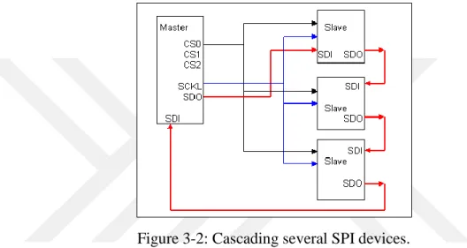
The basic principle how SPI works is provided in Figure (3.2) & Figure (3.3) respectively:
Figure 3-2: Cascading several SPI devices.
The commands and data are serially input to a shift register. The shift register can be of variable length. We can connect the entities in cascade to make it larger bit length, for example, two 9-bit EPROMS can be connected to store 18-bit data [36]. When we connect several SPI devices, they are all treated as one slave, hence their chip select are tied together to make a single chip select. As in Figure (3.2), there are three slave devices connected with a single master device.
Figure (3.3) depicts the situation where the slaves are connected independently with the master. In such case the chip select of all slaves are not tied together, but these are independently controlled by the master device [36].
20
Figure 3-3: Master with independent slaves
The features of the serial peripheral interface is listed below [34]. 16-bit shift register
16-bit receive buffer register (SPIBUF)
16-bit transmit data register (SPIDAT0)
16-bit Transmit data and format selection register (SPIDAT1)
8-bit baud clock generator
Serial clock (SPICLK) I/O pin
Slave in, master out (SPISIMO) I/O pin
Slave out, master in (SPISOMI) I/O pin
Multiple slave chip select (SPISCS[n]) I/O pins (4 pin mode only)
Programmable SPI clock frequency range
Programmable character length (2 to 16 bits)
Programmable clock phase (delay or no delay)
Programmable clock polarity (high or low)
Interrupt capability
DMA support (read/write synchronization events)
21
SPI can be programmed for the following functions [34]:
Clock frequency (SPI module clock/2 through SPI module clock/256)
Character length (2 to 16 bits)
Shift direction (MSB/LSB first)
Clock phase (delay or no delay)
Polarity (high or low)
Delay between transmissions in master mode
Chip select setup and hold times in master mode
Chip select hold in master mode
3.2 Data transfer
In this section, we explain the details for the data transmission starting with the network protocols.
Network Protocols
In communication theory, the definition of protocol is “the special set of rules that end points in a telecommunication connection use when they communicate. Protocols specify interactions between the communicating entities” [38]. In the context of networking, such protocols are more frequently known as “Network Protocols”. Depending on the entities, various network protocols are used. Some of the well-known protocols are:
Internet Protocol
FTP File Transfer Protocol
SMTP Simple Mail Transfer Protocol
22 MTP Media Transfer Protocol
SFTP Secure File Transfer Protocol
SSL Secure Socket Layer
IMAP Internet Message Access Protocol
UDP User Datagram Protocol
For communication among networks, “Internet Protocols (IP)” are widely used. The important types of protocols, which can be used on top of IP, are Transmission Control Protocol (TCP) and User Datagram Protocol (UDP). “TCP is connection oriented, i.e. once a connection is established, data can be sent bidirectional. UDP is a simpler, connectionless Internet protocol”[39].
Both protocols i.e. TCP and UDP are used to send data in the form of a packet. These packets move through intermediary routers before finally reaching their IP address destination [40].
Among the above, TCP/IP is the most widely used network protocol consists of “Transmission Control Protocol (TCP)” in conjunction with “Internet Protocol (IP)” ensures to establish proper communication and exchange of messages among internet points. The TCP is basically used at the “Information Packet Level”.
On other hand, “UDP (User Datagram Protocol) is used primarily for establishing low-latency and loss tolerating connections between applications on the Internet” [4]. When used in conjunction with IP, it is called UDP/IP. Both protocols, i.e. TCP/IP and UDP/IP send short packets of data called datagrams.
23
3.2.1.1 Transmission Control Protocol
TCP is a connection-oriented protocol. It means that the connection is established among the computers or devices prior to exchanging messages. Devices on a TCP connection communicate in a reliable manner thanks to acknowledgment of correctly received messages. If a sender does not receive the acknowledgement message is resends the data. As a result, the data throughput may degrade.
3.2.1.2
User Datagram Protocol
User datagram protocol is a connectionless protocol. It does not require to established connection among the computers or devices prior to exchanging messages. Backward error correction is not provided. The client sends packets of data continuously to the server without knowledge of flawless reception. Therefore, the data rate is higher.
In short, TCP is reliable but not efficient. Whereas, UDP is efficient but not reliable.
Table 3.1: Comparison of TCP and UDP.
TCP UDP
1 Size of header is 20 bytes Size of the header is 8 bytes 2 Two services: (1) Port Number to
differentiate users’ request (2) Checksum with packet for backward error correction
UDP only provides one service. No backward error correction, no sequencing of packets.
3 It provides information from one place to the other in terms of packets. Lost
UDP does not correct the erroneous packets. Such packets are discarded. It
24
packets or erroneous packets are corrected. Some overhead data for error correction, causes latency in communication.
only sends the packets in sequence, due to this reason, it has low latency and more efficient communication. It is therefore ideal to use this protocol in network applications where low latency is required, such as audio and video communications, where loss of some packets does not affect the quality.
4 TCP has heavy overheads. Just to set up socket connection, it requires three packets.
UDP has little overhead by virtue of the fact that it does not do any sequencing of packets, nor it does tracking, nor backward error correction.
Wi-Fi and 802.11 Standards
The Institute of Electrical and Electronics (IEEE), in 1997, developed its first wireless local area network standard, known as 802.11. Wi-Fi is the trademark of the Wi-Fi alliance to certify that their products are compatible with 802.11 standards. For example, a Wi-Fi product with Wi-Fi n certification can communicate with 802.11n devices. Main 802.11 standards are listed below [48]:
802.11a - Wireless network bearer operating in the 5 GHz ISM band with data rate up to 54 Mbps.
802.11b - Wireless network bearer operating in the 2.4 GHz ISM band with data rates up to 11 Mbps.
802.11e - Quality of service and prioritization
25
802.11g - Wireless network bearer operating in 2.4 GHz ISM band with data rates up to 54 Mbps.
802.11h - Power control
802.11i - Authentication and encryption
802.11j - Interworking
802.11k - Measurement reporting
802.11n - Wireless network bearer operating in the 2.4 and 5 GHz ISM bands with data rates up to 600 Mbps.
802.11s - Mesh networking
802.11ac - Wireless network bearer operating below 6GHz to provide data rates of at least 1Gbps per second for multi-station operation and 500 Mbps on a single link.
802.11ad - Wireless network bearer providing very high throughput at frequencies up to 60GHz.
802.11af - Wi-Fi in TV spectrum white spaces (often called White-Fi).
802.11ah - Wi-Fi using unlicensed spectrum below 1 GHz to provide long range communications and support for the Internet of Everything.
Of these, the standards that are most widely known are 802.11b, 802.11g, 802.11n and 802.11ac. In our work, we used 802.11n based chips.
3.2.2.1.1
802.11n
802.11n is also popularly known as "Wireless N". It is the improved version of 802.11g. 802.11n was published in 2009. It supports bandwidths up to 300 Mbps. It has better range/coverage than previous Wi-Fi standards [49].
26
Advantage of 802.11n - High speed and better range;
Disadvantage of 802.11n – High interference with 802.11b & 802.11g based networks nearby due to its multiple signals.
3.3 Comparison of the Wi-Fi modules
Lots of wireless module available in the market that can be suitable and incorporated in our system. However there are many alternative choices available to provide wireless solution such as Wi-Fi, Bluetooth and Zigbee etc [5]. The selection of wireless module depends on the application. Wi-Fi is based on the IEEE 802.11 family. The data rate provided by Bluetooth and Zigbee are much less than Wi-Fi and they are only suitable for short range applications. However, our application does not require long range communication but it demands for high data rate. The data rate provided by Zigbee is 1Mbps whereas Bluetooth provides 1-3 Mbps[5]. Zigbee is suitable for those applications in which there is a need to transfer less data.
Some important factors to consider while selecting module. These factors are the maximum throughput, power consumption and maximum transmission range. Many Wi-Fi modules are now available in the industry today which are very compact and small in size [5]. Using of modules is more logical choice as compare to develop own custom design of wireless interface which takes more time and money. We have reviewed below, several modules which support Wi-Fi.
NRF51822
A Low energy, powerful and compact size SoC by Nordic Semiconductor provides wireless support for applications related to Bluetooth and 2.4GHz protocol stacks. This module contains ARM Cortex M0 processor of 32-bit, which is controlling all the tasks. This system-on-chip communication (SoC) module supports three data rates 1 Mbps, 2 Mbps and 250 Kbps.
27
A wireless protocol is used by this module known as Enhanced Shock Burst (ESB), which enables sending 32 bytes of data in each packet at every 1.2 ms. The module can also use a protocol known as enhanced uESB, which provides higher data rates. uESB can provide up to 1.53Mbps [16], but still it is less than the data rate requirement for our application. Therefore, we did not select NRF51822.
NodeMCU
NodeMCU module is a low cost module for developing wireless applications. It consists of ESP8266 Wi-Fi system-on-chip. It has an ESP-12E version, whose power consumption is low. It is integrated with a low power 32-bit MCU. It also provides network facility. NodeMCU firmware is made of LUA scripting, which makes it easy for the developer to program it quickly by replacing the AT commands [52]. It can provide SPI support as well.
As this module seems perfect for our system, we tested it. We have interfaced the module with an MCP3204 low cost SPI ADC of 4-channels. We have read the analog input values from multiple channels using SPI communication and transmit it wirelessly to the receiving end by utilizing network protocols. We have sent packets of size 1024 bytes. The reason to send 1024 bytes in each packet instead of one byte is to improve throughput. On the remote PC, we have utilized testing tools (i.e. Hercules, Netcat) in order to establish a successful communication. We have used the wireshark application to check the throughput of the transmitting module and to check the time interval among each packet. The data rate of this module was in between 26.5-32 KB/s, which is less than we require. The problem with this module that it transmits each packet at every 50-55 ms, which reduces the overall data rate. Therefore, this module was not suitable to use for our work as well.
28
Particle Photon
Particle photon is a module use for the applications related to internet of things. It consist of no-board Wi-Fi chip (Cypress BCM43362) interfaced with STM32F205 ARM CORTEX M3 Microcontroller, which runs at 120MHz. It has sufficient RAM and flash memory [53]. It provides a WEB based integrated development environment (IDE) for writing and uploading firmware, but it needs the internet connection for uploading the code [54]. Since the local IDE resources or libraries were not enough and the internet connection is compulsory, we decided not to use Particle Photon.
ESP- WROOM-32
ESP-WROOM-32 module includes ESP-32 SoC and it is designed for developing applications in the IoT industry. This chip provides both 802.11b/g/n and Bluetooth connectivity. It contains a flash memory, ROM and Xtensa dual core 32-bit LX6 microprocessor with a clock frequency range from 80MHz-240MHz which can be adjusted by the developer [55][56][57]. The block diagram of ESP-32 is shown in Figure (3.4). By default, both cores are enabled but each one can be enabled or disabled manually. It has an SPI peripheral allowing communication with the external devices. FreeRTOS is the operating system which runs in ESP-32, which allows to prioritize the multiple tasks within a program and provide multitasking. A particular task can be assigned to a specific core by utilizing the function in FreeRTOS. The memory is shared by the cores. Hence, it is possible to write data from one core to memory and read the data using the second core, which improves the performance of the system. In this thesis, we have utilized ESP-WROOM-32 module to take advantage of these functionalities.
29
30
Chapter 4
4 System Realization
We have developed a wireless neural data transmission system that consist of 16 channels microwire arrays that records the neural action potential from the rat brain. The recorded signals are then amplified, filtered and digitized by using an amplifier board (RHD2132) that provides output on SPI bus. As the board performs all SPI signaling with LVDS signals, so they are converted in to CMOS signals using CMOS-LVDS converter. Wireless communication module that supports IEEE 802.11n standard protocol is used that consist of on-chip microcontroller. It collects the data from the board by SPI communication and stores data in a buffer, and then pushes the data to 802.11n transmitter. Receiver displays received data and performs data logging to stores the data for future analysis. The architecture of our system is shown in Figure (4.1).
In addition, we have created the designs of silicon based micromachined microelectrode array of 8 and 32 channels for recording the neural signals. It consists of multiple electrodes on the probe with uniformly spaced.
31
Figure 4-1: System architecture of Wireless Neural Recording System.
4.1 Microelectrode Array (MEA) Development
Prior to the designing of Microelectrode arrays (MEAs) the geometry and shape of the MEA and probe shank must be decided as it may have a significant impact on its mechanical strength. Silicon is the material of the probe in MEA, which has a yield strength of 7 GPa. So the stress value must not exceed beyond the yield strength otherwise it may led to deformation of the probe and it may fracture. The probe must have strong mechanical structure[2] that can penetrate easily in to the motor cortex without damaging the brain tissues. The length of the probe must be greater than 1mm so that it can penetrate in to the deep brain structures. In this thesis we have followed the same design approach as in [2]. The length and width of the probe are 3mm and 100um. Distance between the probe is kept at 200um and the width of the probe tip is 5um. The thickness of the probe is kept at 25um. The distance between the traces are 10um. We have developed 24 designs for 8 and 32 channel recording in which all of them having total eight shanks. Out of 24 designs, the first four designs have eight channels and rest of them have 32 channels. 8-channels recording
32
microelectrodes have one electrode on each shank. 32-channels recording microelectrodes have four electrodes on each shank, which are separated by 50um. The width of the probe tip is 5um. The width of the trace is 10um, which is used to connect recording site with the recording pad. All designs have different probe lengths, probe widths with different inter-shank spacing. 11 designs have a recording electrode area of 169𝑢𝑚2 and another 11 designs have the recording electrode area of 400𝑢𝑚2. The last 2 designs have recording electrode area of 1600𝑢𝑚2. In [2], the area of the recording site is 144𝑢𝑚2. The length and width of the probes in all the designs are kept in a range of 2-10 mm and 50-200 um. The inter-shank space of all designs are in range of 250-600 um. The distance among the traces on the shank should be kept at 10um in order to avoid the cross talk [2]. Thickness of the probe is varied by using SOI wafer of different device layer thickness.
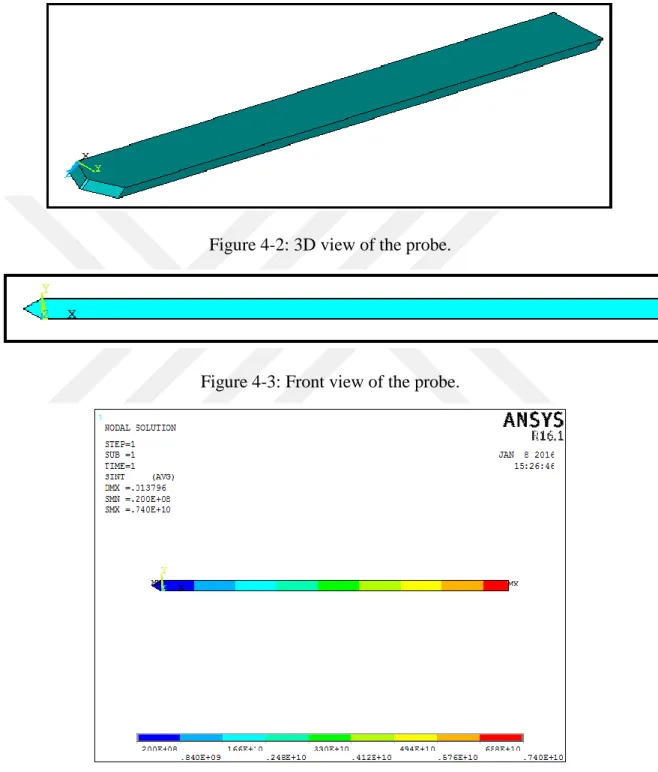
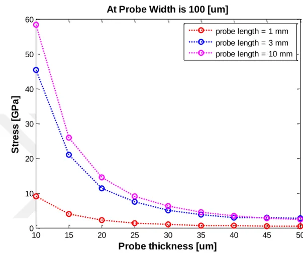
Mechanical strength of the probes was checked via simulations. Simulations are performed using ANSYS software which allows the development of 3D models and test models in an virtual environment prior to fabrication [59]. As a first step, we have developed a 3D model of a single probe. Width and thickness of the probe is 100um and 25um. Figure (4.2) and Figure (4.3) shows the 3D view and the front view of the probe. The 24mN force applied on the tip of the probe in the z-direction to check the stress on probe as shown in Figure (4.4). Around 1mN force is required for probe insertion into the brain [60]. The value of stress was 7.4GPa, which is slightly higher than the requirements. We have performed simulations of the designs by keeping the probe thickness constant at 25um and varying the probe width from 20um to 200um, while in the second simulation, the probe width is kept constant at 100um and varied the probe thickness with in a range from 10um to 50um. We have created both the plots using MATLAB software as shown in Figure (4.5). The first plot shows that stress on the probe decreases by increasing the probe width. While second plot shows that the stress on the probe decreases by increasing the probe thickness. In Figure (4.6), we have checked the value of the stress on the probe with different probe lengths i.e. 1mm, 3mm and 10mm. These simulations provides the range of values that would be appropriate for our designs. We have developed 24 designs using K-Layout software. Parameters of all the designs are shown in Table (4.1). Figure (4.7) shows the mask of all 24 designs. Figure (4.8) shows a design of microelectrode. Figure (4.9) shows all shanks of the single MEA. Figure (4.10) shows the view of an individual shank out of 8 shanks, arrangement of individual
33
electrode on single shank and tip width. Figure (4.11) shows the recording pads and traces that connects the electrodes to the recording pads.
Figure 4-2: 3D view of the probe.
Figure 4-3: Front view of the probe.
34
Figure 4-5: Stress curves, the first plot shows the varying stress values while changing probe width (um) and keeping probe thickness constant. The second plot shows the varying
35
Figure 4-6: Stress values with varying probe thickness of different length of the probe.
10 15 20 25 30 35 40 45 50 0 10 20 30 40 50 60
Probe thickness [um]
S tr e s s [ G P a ]
At Probe Width is 100 [um]
probe length = 1 mm probe length = 3 mm probe length = 10 mm
36
37
Figure 4-8: Design of microelectrode array.
38
Figure 4-10: Closer view of the individual shank out of 8 shanks, arrangement of electrodes on shanks and tip width.
39
40
4.2 Recording System Development
In this section, we provide the details of the recording system we develop stating with the amplifier board. RHD2132 amplifier board developed by Intan Technologies is made for recording electrophysiological signals. The amplifier board consists of 32 amplifier channels, high speed multiplexer, an analog-to-digital converter with a resolution of 16 bits. It has an SPI interface and works at a maximum frequency of 24 KHz. Amplifier board is hard-wired with the Intan chip signal LVDS_en to high voltage, which makes the chip perform all SPI signaling with Low-voltage differential signaling (LVDS) signals. Therefore, we have used CMOS-LVDS converter (SN65LVDT41, TEXAS INSTRUMENTS). Figure (4.12) and (4.13) shows the block diagram and internal logic diagram of SN65LVDT41. LVDS signaling works much better than CMOS signaling at high speed over long cables. Figure (4.14) and Table (4.3) shows the connection diagram and pins of (ESP-32 board, SN65LVDT41, RHD2132 Amplifier board). Figure (4.12) and (4.13) shows the block diagram and internal logic diagram of SN65LVDT41. LVDS signaling works much better than CMOS signaling at high speed over long cables. Figure (4.14) and Table (4.3) shows the connection diagram and label of connection pins of ESP-32 board, SN65LVDT41 and RHD2132 Amplifier board. This chip supports sampling 32 amplifier channels at 30 KSPS each. We have used 16 channels microwire arrays for recording the neural action potentials.
The ESP-32 module developed by Espressif, which supports IEEE 802.11 b/g/n standard protocols. It consists of dual core Tensilica LX6 microcontroller. It has SPI bus. It is possible for ESP-32 to read digitally converted data from RHD2132 amplifier board by using SPI communication protocol.
This chip has 64 on-chip RAM and ROM registers. Each register is of 8-bits in length. It is required to write the values in RAM registers to make the chip operational. Then it must be calibrated for necessary clock cycle generation.
Analog to digital converter sampling rate is set by writing values in variables of 5-bits length in register 1 (ADC buffer bias) and register 2 (Mux bias). The sampling rate is set at 700
41
KSPS. Table (4.2) shows the set the values for selecting different sampling rates. The upper and lower cutoff frequencies of the chip ranges from 100 Hz to 20 KHz and 0.1 Hz to 500Hz. We have set the upper and lower bandwidth at 7.5 KHz and 150 Hz of the amplifiers by writing values in register 8-11 and register 12-13. Table A.1 and Table A.2 in appendix A that shows all the values to select different lower and upper bandwidth of the amplifiers. Since we are using 16 amplifier channels, so it is possible to power off the remaining amplifier channels by setting values in register 14-17, for reducing the power consumption of the system. See Table A.3 in appendix A.
Table 4.2: ADC sampling rate [33].
Figure 4-12: Block diagram of Wi-Fi module, CMOS-LVDS converter and Amplifier board.
42
Figure 4-13: Internal logic diagram of SN65LVDT41
Figure 4-14: Connection diagram of (ESP-32 board, SN65LVDT41 and RHD2132 Amplifier board).
43
Table 4.3: Connection pins of RHD2132 Amplifier board (AFE), CMOS-LVDS converter and ESP-32 board (MCU + Wi-Fi module)
We have reset the output of digital high pass filterof each channel by writing the channel number in a register with LSB set to high as shown in Table (4.4). Then we have performed analog-to-digital conversion in the same manner by writing channel number but resetting the LSB bit. Amplifier board sends the converted result to the Wi-Fi module after two commands with MSB first.Table (4.5) shows how the board sends the converted value back to module.
Table 4.4: Command for performing analog-to-digital conversion[33].
Table 4.5: Result sent back by RHD2132 to module [33].
To check the proper operation of the amplifier board. We have interfaced the board with the module that is serially communicating with the PC using the USB COM port. We have used
44
a serial terminal application (putty) on PC to check the converted value sent by amplifier board. It was working properly.
It is required to sends the recorded signals wirelessly to the remote PC. We have used UDP (User Datagram Protocol) network protocol to transmit the packets of data. We have used PC as a server and ESP-32 module as a client. UDP functions are utilized in ESP-32 module that requires IP address, port number of the server and the payload data to send. We have created a UDP socket at the server. For the wireless networking, an access point (Netis Router WF2414) is utilized. We have connected the server PC to the router. We have provided SSID of an access point to the client.
We have used Hercules utility (works on windows) as a testing tool use for network applications. It is used for checking the packets of data received by the server that was sent by the client using UDP communication. According to our test, the module was successfully sending the data. Figure (A.1) shows the graphical user interface (GUI) of Hercules in appendix A.
In order to check the maximum throughput of the device using UDP, we have generated triangular wave of different references for 16-channels and sends 10 MB of data to the server PC and kept each packet size of 1Kbyte (1024 byte). Each packet contains 64-bytes of data for each channel. After sending the data to the destination, we have performed analysis on the server PC by using a packet sniffer software known as wireshark. We have used this software to check the total number of packets captured and lost, time interval among each packet and total time taken to capture the 10 MB of data at the receiving end.
The framework inside the ESP-32 i.e. ESP-IDF works on FreeRTOS (real time operating system). A scheduler is responsible for multitasking, which runs the task according to the priority assigned to it. FreeRTOS provides a function to utilize two cores and split tasks on two separate cores. The first step is creating tasks and assigning priority to them. Once it is created then scheduler executes the tasks based on the given priority [61].
We decided to use16 channels microwire array implanted on the rat brain to record data. The array is connected with the RHD2132 amplifier board that amplifies the neural signals by 45.7 dB. The sampling rate of each channel is set at 25 KSPS. The board provides digitized
45
output on SPI bus. We have utilized dual core functionality and assigned separate tasks to cores. ESP-32 module communicates with the RHD2132 amplifier board at the frequency of 24 MHz. The first core reads the converted data from the amplifier board using SPI protocol and store data in buffer. Second core reads that data from the buffer and pushes to IEEE 802.11n standard. The packet size is decided to be 1 KB. Total data rate required is 6.4 Mbps.
We decided to use LabVIEW software at the server end. LabVIEW is a graphical programming language. It is easy to use for taking measurements and analyzing them. We have created UDP socket on LabVIEW by using data communication toolbox for network communication. Remote PC is set as server and ESP-32 module as client. We have developed an algorithm on LabVIEW to count the total bytes and packets received by utilizing Mathscript RT tool. It can execute mathematical commands used in MATLAB by doing textual programming inside the frame in block diagram window. A code is written inside the frame that checks the length of the received data coming at the input of the frame, which indicates the incoming number of bytes. The total number of received packets can be counted via the system. Block diagram of the code is shown in Figure (4.15). We enabled data logging on the same program by writing it in a TDMS file. Since MATLAB uses CSV files easily, we have developed a program on LabVIEW from TDMS to CSV conversion. Figure (4.16) and Figure (4.17) shows the block diagram and front panel. On the front end, we have to provide the file path of the data written in TDMS format. After file format conversion, data is imported into MATLAB. We have written a small code in MATLAB as shown in Figure (4.18) for converting all consecutive two bytes of data in to 16-bit integer values and sorting all the values according to their channels.
In LabVIEW, whenever it reads data it gives string output. As strings is the array of characters and each character is of 8-bit (1-byte), the character arrays are converted into unsigned byte arrays. Each sample value that RHD2132 provides is of 16-bit (2-byte). An array of 1024 byte consist of 512 sample values. These values are splitted according to channels. By assigning output variable on the frame, a plot can be created of each channel to visualize the data[65]. Data-logging is performed for each individual channel. The block diagram and front panel (GUI) of 16-channel UDP server are shown in Figure (4.19) and (4.20). In the next section we provide the details of an experiment, which is performed on an awake rat by
46
recording neural action potentials from 16-channel microwire arrays with each channel sampling frequency is 25 KHz
Figure 4-15: Block diagram of UDP server that counts the total number bytes and packets received and writes data on TDMS file.
47
Figure 4-16: Block diagram that converts TDMS file to CSV file.
48
Figure 4-18: Code written in MATLAB for converting bytes in to values and sorting data according to their Channels.
49
50
Chapter 5
5 Experimental Results
5.1 Preliminary Results
To test the recording system, 10000 packets (10 MB data) are sent multiple times using UDP protocol to check the overall performance. We monitored the loss of packets, time interval among each packet and total time to receive all the packets. Packets are captured using Wireshark application as shown in Figure (5.1). Results show that there is no packet loss, which is marked in a red rectangular outline. It takes overall 12.792 seconds to capture 10MB of data. Majority of the packets have taken ≤ 2ms. Figure (5.2), shows the histogram plot that provides the statistical information of the total captured packets that shows the frequency of the captured packets in equally size time intervals [66]. We repeated the experiment and results show that we have lost just few packets. Results of the repeated experiments are shown in Figure (A.2), Figure (A.3) and Figure (A.4) in appendix A. In Figure (A.2), 4 packets are lost. In Figure (A.3), 3 packets are lost. In Figure (A.4), there is no packet loss. We have performed data logging on LabVIEW and stored results for each channel. Figure (5.3), shows the plots of triangular wave of the first 4 channels out of 16 channels with different references on LabVIEW. The transmitted and received data are the same.
For testing the program that we wrote on LabVIEW for counting total number of bytes and received packets, 10000 packets are sent. The result shows that we have lost just one packet. We checked the code on MATLAB for 2 bytes to 16-bit integer conversion and sorting the
51
values with respect to their channels. The code is working and test triangular waves are received as shown in Figure (5.4), which shows the plot for first 4 channels out of 16 channels.
5.2 Results from the Experiment on a Test Animal
We have performed recording from an awake rat from 16-channels using microwire arrays connected to the RHD2132 amplifier chip as shown in Figure (5.5). Figure (5.6) shows the CMOS-LVDS converter board connected with the Wi-Fi module. Each channel is sampled at a rate of 25 KHz. 10 MB of data is sent from the rat to the remote PC multiple times to check the packet loss and then we have plotted histograms of each trial. Figure (5.7) shows the plot of the recorded neural spikes from the 7th channel out of 16 channels. We used wireshark application again to measure the data rate and packet arrival intervals. Figure (5.8-5.12) shows the histograms of each trail to observe the total received packets and maximum time taken by the packets. The distribution of packet arrival-intervals are plotted, which shows the mean and standard deviation as shown in Figure (5.13). Results show that, most of the received packets has a delay ≤ 2ms. The data rate of the overall system was at 6.4 Mbps, which satisfy experiment requirements.
52
Figure 5-1: 10000 packets (10MB of data) captured in Wireshark.
53
Figure 5-3: Front panel of UDP server that counts the total number bytes and packets received and writes data on TDMS file.
Figure 5-4: Plot for 1st four channels on MATLAB.
100 110 120 130 140 150 160 170 180 190 200 3.29 3.3 3.31 3.32 3.33 3.34 3.35 3.36 x 10⁴ D ig it a l o u tp u t
Plots for first 4 Channels
Channel 1 Channel 2 Channel 3 Channel 4
54
Figure 5-5: Microwire array implanted in the rat brain and RHD2132 amplifier Chip.
55
56
Figure 5-8: Histogram of 1st trail.
57
Figure 5-10: Histogram of 3rd trail.
58
Figure 5-12: Histogram of 5th trail.

![Figure 2-2: Basic structure of silicon based Michigan probe [1][3].](https://thumb-eu.123doks.com/thumbv2/9libnet/5464643.105562/21.918.195.704.483.829/figure-basic-structure-silicon-based-michigan-probe.webp)
![Figure 3-1: Schematic diagram of RHD2132 chip[33].](https://thumb-eu.123doks.com/thumbv2/9libnet/5464643.105562/28.918.169.853.113.715/figure-schematic-diagram-of-rhd-chip.webp)


![Figure 3-4: Block diagram of ESP32 SoC [58].](https://thumb-eu.123doks.com/thumbv2/9libnet/5464643.105562/39.918.151.750.102.617/figure-block-diagram-esp-soc.webp)