Nanotechnology
PAPER
Electroless synthesis of 3 nm wide alloy nanowires
inside Tobacco mosaic virus
To cite this article: Sinan Balci et al 2012 Nanotechnology 23 045603
View the article online for updates and enhancements.
Related content
Improved metal cluster deposition on engineered TMV
Sang-Yup Lee, Elizabeth Royston, James N Culver et al.
-Biofabrication methods for the patterned assembly and synthesis of viral nanotemplates
K Gerasopoulos, M McCarthy, P Banerjee et al.
-Integration of plant viruses in electron beam lithography nanostructures
Jose M Alonso, Thierry Ondarçuhu and Alexander M Bittner
-Recent citations
Alexander M. Bittner
-DNA mold templated assembly of conductive gold nanowires
Türkan Bayrak et al
-Helical plant viral
nanoparticles—bioinspired synthesis of nanomaterials and nanostructures
Kannan Badri Narayanan and Sung Soo Han
1Max-Planck-Institut f¨ur Festk¨orperforschung, Heisenbergstraße 1, D-70569 Stuttgart, Germany 2Max-Planck-Institut f¨ur Metallforschung (now MPI f¨ur Intelligente Systeme), Heisenbergstraße 3,
D-70569 Stuttgart, Germany
3Universit¨at Stuttgart, Biologisches Institut, Abteilung Molekularbiologie und Virologie der Pflanzen,
Pfaffenwaldring 57, D-70550 Stuttgart, Germany E-mail:[email protected]
Received 3 September 2011, in final form 24 November 2011 Published 4 January 2012
Online atstacks.iop.org/Nano/23/045603
Abstract
We show that 3 nm wide cobalt–iron alloy nanowires can be synthesized by simple wet chemical electroless deposition inside tubular Tobacco mosaic virus particles. The method is based on adsorption of Pd(II) ions, formation of a Pd catalyst, and autocatalytic deposition of the alloy from dissolved metal salts, reduced by a borane compound. Extensive
energy-filtering TEM investigations at the nanoscale revealed that the synthesized wires are alloys of Co, Fe, and Ni. We confirmed by high-resolution TEM that our alloy nanowires are at least partially crystalline, which is compatible with typical Co-rich alloys. Ni traces bestow higher stability, presumably against corrosion, as also known from bulk CoFe. Alloy
nanowires, as small as the ones presented here, might be used for a variety of applications including high density data storage, imaging, sensing, and even drug delivery.
S Online supplementary data available fromstacks.iop.org/Nano/23/045603/mmedia
(Some figures may appear in colour only in the online journal)
1. Introduction
Alloy formation is a very established way to tune many properties of metals. For example, the magnetic coercivity of ferromagnets depends heavily on alloying, and in fact most commercial permanent magnets are based on alloys. On the nanometer scale alloying is much less established—most applications for nanoparticles are based on pure metal particles, while most applications for bulk metals are based on alloys. On the other hand, nanostructures have attracted great interest in recent years due to promising applications in data storage, imaging, sensing, and even drug delivery [1–7]. Probably most advanced are the fields of data storage and sensing, although usually wires with diameters well above 4 New address: Department of Physics, Advanced Research Laboratories,
Bilkent University, 06800 Ankara, Turkey.
5 New addresses: CIC nanoGUNE Consolider, Tolosa Hiribidea 76, E-20018
Donostia, Spain. Ikerbasque, Basque Foundation for Science, E-48011 Bilbao, Spain.
10 nm are employed. Clearly, extremely small wires and alloy structures will broaden the scope enormously.
For extremely small metal and alloy nanostructures, with typical dimensions below 10 nm, practically all physical properties differ significantly from their bulk counterparts. For example, magnetic metal (and oxide) particles can become superparamagnetic at room temperature (RT), allowing for fine-tuning of their magnetic properties [2]. Additionally, exciting basic questions can be addressed, for example how to create or stabilize ferromagnetic structures in extremely small structures. Such structures can be synthesized by vacuum deposition, focused ion beam milling, electron beam lithography, high temperature wet chemical synthesis, or electrochemically [1–7]. Electrodeposition works under ambient conditions, it requires rather simple tools, and it is well established also for alloy formation. However, it requires the presence of an electrode. Whenever such a surface is not available, or when effects such as predominant deposition at sharp features have to be avoided, electroless
Nanotechnology 23 (2012) 045603 S Balci et al
Scheme 1. Synthesis of extremely small diameter (∼3 nm) alloy nanowires in the tubular channel of TMV particles. The particles are isolated from plants, wet chemically sensitized/activated with Pd(II) catalyst, and metallized with Co(II) and Fe(II) in suspension.
deposition (ELD) can offer an alternative [3, 8–24]. While the ELD of Cu and Ni has been very well investigated since they are employed for various products, many other metals qualify for investigation too [24]. High-tech and nanoscale structures are in some cases already well established, as shown by Cu deposition for microchip interconnects [9], and other superconformal coatings [10]. ELD is suitable for the production of extremely small particles and wires; the limit is below 4 nm [11–20] (in a broader definition, even the standard chemical reduction routes for clusters containing merely a few metal atoms could be called ELD).
We believe that a big challenge for nanostructure synthesis is the shift from pure metals to alloys, whilst preserving the size of the structures. This can be very conveniently addressed with ELD, by using a mixture of metal salts for codeposition, e.g. CoFe from dissolved Co(II) and Fe(II). Such processes are well known from electrodeposition, where the synthesis of various alloys of Ni, Co, and Fe is established. Note that the bath stoichiometry (of the educt metal ions) is not generally preserved in the deposit, so the problem of chemical analysis on the nanoscale has to be addressed. This is clearly evident for Fe: its very low redox potential should not allow it to deposit more than traces, while the deposition rate is high for pure Co. However, when Co(II) is mixed with Fe(II), both elements can be deposited to form alloys, i.e. their deposition rates are very similar. One of the most important applications for CoFe alloys is in thin, soft magnetic layers for magnetic reading heads, which are today still produced by vacuum deposition techniques.
We here report the electroless synthesis of ∼3 nm diameter CoFe and CoFe(Ni) alloy wires within the central channel of Tobacco mosaic virus (TMV) particles (virions). The electroless synthesis of the alloy nanowires involves isolation and purification of virus particles from tobacco plants, pretreatment with aqueous Pd(II) (‘sensitization’, i.e. coating with Pd catalyst particles), and finally the metallization in an aqueous solution that contains the desired metal ions, i.e. Co(II), Fe(II), Ni(II) (scheme 1). It is established that the exclusion of phosphate directs the sensitization and hence the metallization exclusively to TMV’s interior channel [12–17], which is only 4 nm wide, and a relatively new template for nanowires [12–17, 20].
One of the best known templates is porous alumina [18], while extremely small diameters can be reached in micelles (<2 nm) [25], or in microtubuli [21,22].
As in the case of other metallizations we had developed [12–18] (see also section 4), we first removed unwanted ions such as phosphate from the TMV suspension. The sensitization in Pd(II) required high concentrations of Cl−and H+to produce Pd particles that fit inside the channel, and washing with water to remove surplus Pd(II) (scheme1). The ELD bath is based on dimethylamine borane (DMAB) as reductant, and succinate as complexant. It is stable at ambient conditions and based on the autocatalytic reactions (1), valid for M = Fe, Co, Ni:
M(II) + BH3+H2O → M + BH2(OH) + 2H+
M = Fe, Co, Ni; redox potentials Fe(II) −0.44 V, Co(II) −0.277 V, Ni(II) −0.250 V.
(1)
BH2(OH) reacts in a similar way to BH(OH)2, and
finally to B(OH)3. The source of BH3 is most conveniently
dissolved DMAB, which was shown to be sufficiently active to induce fast growth of nanowires [12, 13, 17]. ELD of Ni generally produces coatings of lower porosity and more uniform thickness than electroplated Ni [24]. Because of this property, ELD Ni films are effective corrosion protecting agents. In fact, Ni can be added to Co, Fe or CoFe alloy films to improve the corrosion resistance [26]. Myung et al found that the corrosion resistance of CoFe ELD films is an order of magnitude lower than that of CoNi and NiFe films [27]. In a similar way, we introduced Ni into CoFe by simply adding Ni(II) to an ELD bath containing Co(II), Fe(II), succinate, and a borane compound (see experimental part for details). The produced bath is stable and can be used for depositing CoFe(Ni) on Pd-sensitized surfaces. For instance, Pd-sensitized glass is easily coated with a shiny film of CoFe(Ni).
2. Results and discussion
After mixing ELD bath and sensitized virions, we observed some bulk deposition on the reaction vessel wall, which we used as an indication of successful deposition, removed
Figure 1. (a) TEM micrograph of CoFe alloy nanowires within the channel of a TMV particle (dark gray). The black line in the center corresponds to an alloy wire of ∼3 nm in diameter and approximately 100 nm in length. In the lower part of the same virion a second small nanowire (∼10 nm long) is located. Another short virion (∼100 nm long) is attached to the lower portion of the metallized virion.
(b) High-resolution TEM image of a CoFe nanowire inside TMV. Crystal planes of various orientation and spacing are visible, all
compatible with various orientations of CoFe. The image was calibrated by imaging Au particles at the same magnification. (c) TEM image of two short CoFe(Ni) wires located in a single virion cavity. The dark nodule at the bottom part stems from bulk deposition of the alloy.
aliquots of the virus suspension, and analyzed them with TEM. Metallized TMV is characterized by wires with diameters slightly below the TMV channel diameter (4 nm) (figure1). From our experience with Co wires, it is obvious that not only Pd (our sensitizer), but also Co can catalyze the deposition reactions inside the TMV channel, which is the prerequisite for wire formation, starting from a single catalytic center [12–17]. While we do not expect that Fe is active [28], a Co-rich CoFe alloy should perform well, too. Figures1(a) and (b) show CoFe wires in TMV, and CoFe(Ni) wires are seen in figure1(c). Most of the wires are ∼3 nm wide, irrespective of their chemical composition. The wires comprise only small crystalline areas, which are not useful for elucidating details: For example, figure1(b) shows planes with a spacing of about 0.20 nm, which would fit to Co-hcp (001), Co-fcc (111) (both 0.204 nm), but also to CoFe-bcc (110) (0.200 nm) (see also supporting information available at
stacks.iop.org/Nano/23/045603/mmedia). Unfortunately, we produced a small amount of nodules (large nanoparticles) with >20 nm diameter (e.g. figure 1(c) shows a part of a nodule as a black semicircle at the left bottom). This does not allow meaningful magnetometry or (bulk) elemental analysis of our samples, different from purified Ni tubes grown on the outer coat of TMV [18]. The nodules most
likely result from the hydrolysis of surplus catalyst PdCl2−4 to O(H)-bridged Pd(II) units; the ELD process reduces them to Pd nanoparticles, on which the alloy can grow to thick layers. Different from the Pd(II) inside TMV, the diffusion of dissolved species to/from the particles is very fast, hence even small amounts of free catalyst result in considerable alloy mass concentrated in nodules. Apart from this phenomenon, ELD is highly selective for the TMV channel: deposits on the outer coat of TMV are rarely observed. This is equally true for stepwise adsorption–reduction cycles that were used to produce Pt alloys inside TMV [20], and for deposition of nanoparticles inside the channel [11–17]. Figure 1(c) is an example for two short wires in a single channel. In accordance with the proposed mechanism [29], three wires were never found: once two wires grow inside a single cavity, the solution encapsulated between the two wires contains an insufficient number of metal ions to produce a third wire.
While we found wire structures in the CoFe(Ni) samples on TEM grids even after many weeks in air, the CoFe wires deteriorated already after two weeks (no nanowires could be detected). On the TEM grid surface, only particles a few nanometers in diameter were found, but no more virion-like structures. We postulate that air oxidation (corrosion) destroyed the CoFe structures. In contrast, CoFe(Ni), pure Ni,
Nanotechnology 23 (2012) 045603 S Balci et al
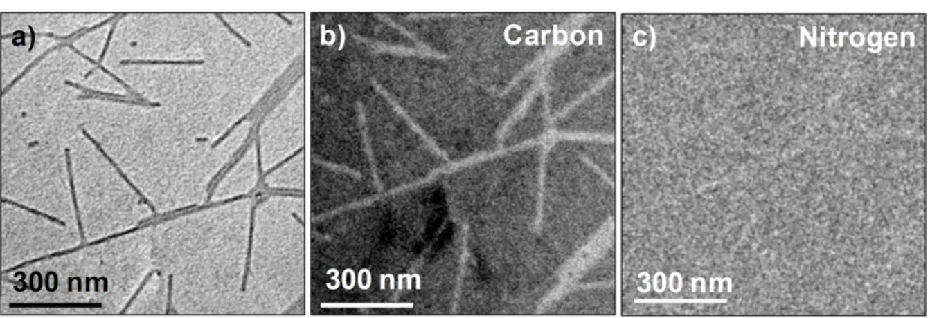
Figure 2. Elemental maps of pristine virus particles by EFTEM. (a) Pristine TMV particles imaged by TEM. No staining procedure was applied. The virions are randomly distributed on the TEM grid, but show linear and lateral aggregation. (b) Same area imaged with carbon EFTEM. The carbon content of the virions yields a good contrast, despite the carbon-rich background. Drift has moved the imaging area slightly. (c) Nitrogen EFTEM imaging of the area shown in (a).
and pure Co wires are all stable [12–17]. Hence Ni appears to work as a corrosion inhibitor for CoFe. In fact, Myung et al studied the influence of Ni on bulk CoFe alloys, and found that corrosion resistance of electrodeposited CoFe films was an order of magnitude lower than that of CoNi and NiFe films, meaning that Ni plays a crucial role in increasing the corrosion resistance [27]. Indeed we found that this result, based on bulk phases, can be scaled down to 3 nm since our CoFe(Ni) wires were much more stable than our CoFe. Naturally, the complex nature of the nanoscale system does not allow quantitative calculations on the corrosion. However, possible mechanisms are based on water, or on oxygen dissolved in water. Aqueous solutions can easily reach the TMV channel from the viral orifices, but oxygen can additionally diffuse through the protein coat (7 nm thick sheath), which proceeds on the timescale well below 1 ms [30].
For a local chemical analysis we employed energy-filtering TEM (EFTEM), which is usually applied for rather large nanostructures (>10 nm), although atomic resolution is possible. We tested EFTEM first for pure virions, which are known to show TEM contrast even without staining [18]. Here we found C edge contrast in EFTEM, for samples adsorbed on carbon film TEM grids (large C background): figure2(a) shows TEM of TMV particles (dark gray lines). TMV particles are in most cases aggregated side-to-side and end-to-end. The electron spectroscopic image (figure 2(b)) proves the presence of carbon in the TMV particles (carbon K-edge at 284 eV), and the carbon map closely reflects the TEM image. Of course TMV contains also N and O; but O (K-edge at 532 eV) was not observed, and N (K-edge at 401 eV) only with extremely low signals in elemental maps (figure2(c)).
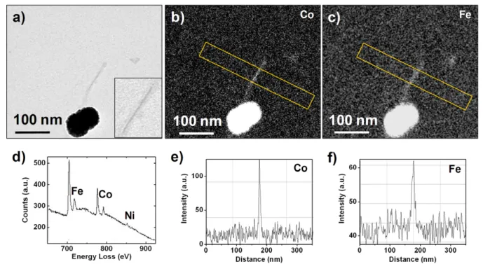
For EFTEM experiments, the instrumental drift can attain much more relevance than for TEM: e.g. during recording figure2(b), the carbon map shifted slightly, which is a result of thermal effects that cause the sample to move during electron beam exposure. Figure3was recorded in a similar way from an alloy wire, after better equilibration. The TEM image shows a nanowire (dark line) within the central cavity of a single TMV particle, figure3(a). The gray-shaded region with
200 nm length and ∼20 nm diameter corresponds to a part of a virion attached to a large metallic nodule (∼100 nm in diameter), while the dark line within the particle indicates the nanowire of ∼3 nm width and 100 nm length. Figures 3(b) and (c) display the electron spectroscopic images, revealing the Co and Fe elemental distribution across the single virion. They were obtained from the element-specific signals at the Co L2,3 and Fe L2,3 edges, respectively (see figure3(d) for
an electron energy loss spectrum of the elements). The Ni elemental map did not show any intensity, indicating that the amount of Ni in the nanowire was very low (below our noise level). The length of the nanowire in figure3(a) is reproduced in both the Co and Fe elemental maps (figures3(b) and (c)), and the large nodule at the bottom of the image follows the respective TEM image, too. The line scans perpendicular to the nanowire’s long axis in the Co and Fe maps are shown in figures 3(e) and (f), respectively; the peak widths of the EFTEM signals are two to three times larger than the true (TEM) width. An analysis of the spectra [12–17, 31, 32] yields ∼90% Co and ∼10% Fe for large area imaging (which also counts the big nodules), as well as for single wires. The nanowires remained unchanged for many days in air, such that successive experiments did not suffer from destruction of the wires. Only after several weeks in air we were unable to find any structures (see above).
Figure 3(d) is an electron energy loss spectrum of CoFe(Ni)-metallized TMV. The illuminated area used for the energy loss spectrum acquisition contained a nanowire within the central channel of the TMV particles and also some metal agglomerates produced during electroless deposition. Literature values of ionization edges of Fe, Co, and Ni show that the energy loss peaks at 854 eV for Fe, at 779 eV for Co, and at 854 eV for Ni can be attributed to the corresponding elements (see also supporting information available atstacks. iop.org/Nano/23/045603/mmedia) [31]. The spectrum shows sharp ‘white lines’ that correspond to the L2and L3edges of
Ni, Co, and Fe [32].
The 90:10 ratio between Co and Fe shows that not all bath constituents are deposited, although they can be deposited (thermodynamically allowed and also sufficiently fast) in the
Figure 3. Elemental maps of a single CoFe nanowire. (a) TEM micrograph of a CoFe nanowire within the central channel of a TMV particle. The dark line in the center corresponds to the wire of ∼3 nm in diameter and ∼100 nm in length. The dark gray region around the nanowire is the TMV particle. The inset shows the zoom-in view. (b) Co and (c) Fe maps from the same area shown in (a). (d) Energy loss spectrum of a CoFe(Ni) sample showing the L2,3ionization edges at characteristic energy losses. (e), (f) Line scans perpendicular to the nanowires in (b), (c), respectively. Intensity data are summed and plotted as single traces. The widths of the peaks are 6 nm for Co and 10 nm for Fe.
absence of the other constituents. In other words, ELD of a mixture of metals is not (or not generally) an additive process with independent reduction of the metal ions; rather the reactions influence each other. One should note that even for the independent reactions, the kinetics differ very much for each element, and one would expect that the element with the most negative reduction potential, Fe, shows the smallest deposition rate. The reduction of Fe(II) to Fe(0) in itself might be surprising since the redox potential is much lower than that of Co(II) and Ni(II) (see reaction (1)). One would thus expect slow kinetics; however, Nakanishi et al reported ELD from Fe(III) with DMAB, producing Fe(0) on amine-terminated surfaces [33]. We, too, find a surprisingly high deposition rate of Fe (1/9 of that of Co), an indicator of the interdependence of the reduction of Co(II) and Fe(II). Similarly, the small amount of the more noble Ni can only be explained by (adverse) kinetic effects.
The results for the chemical composition can also be discussed in the framework of our high-resolution TEM (HRTEM) experiments, when literature data on alloy structures are considered. From ELD one would expect exclusively crystalline alloys. In fact, ELD Co films show the usual hcp structure (ABABAB stacking), but can also attain fcc (ABCABC stacking), e.g. for high temperatures or in nanostructures [34]. Bulk CoFe, too, has the hcp structure for small amounts of Fe (.2%), but bcc for &21% Fe. Between these values, the phase separates into hcp Co0.98Fe0.02 and
bcc Co0.79Fe0.21 [35]. Hence addition of small amounts of
Fe changes the interatomic distances and even the crystalline structure of Co. The magnetic properties change too [34].
When adding trace amounts (<2%) of Ni, the properties of Co and CoFe do not change significantly. For example, Co with up to 2% Ni is still hcp-packed [35]. We found many parts of our wires crystalline, but also parts that yielded no atomic planes. An example is given in figure 1(b) (see supporting information for more images available at stacks. iop.org/Nano/23/045603/mmedia), a single wire with atomic planes (parallel streaks) of various orientations, which would fit to phases of Co and CoFe [36]. Different from other metals [20], the CoFe planes make a rather small angle with the wire axis. However, one should be aware that nanowires can also show non-bulk phases since a large fraction of the metal atoms is located on the wire surface, which is in our case the interface with the virus channel. Note that traces of Ni do not change the crystal structure of Co or CoFe, so they should play no role in HRTEM either.
3. Conclusions
In summary, we showed that very small diameter (∼3 nm) CoFe alloy nanowires can be grown within the central channel of the Tobacco mosaic virus by simple wet chemical electroless deposition. Energy-filtering TEM investigations at the nanoscale revealed that the electrolessly synthesized wires are alloys of Co, Fe, and Ni. We confirmed by high-resolution TEM that our alloy nanowires are partially crystalline, which is compatible with typical Co-rich alloys. Ni traces bestow higher stability, presumably against corrosion, as also known from bulk CoFe. It is an exciting question, with far-reaching consequences for the many known metal
Nanotechnology 23 (2012) 045603 S Balci et al
nanoparticles, whether corrosion properties scale right down to the atomic scale. Wires as small as the ones presented here can be used for new types of high density data storage. To this end, alignment and soft lithography techniques allow us to create arrays on a variety of substrates [37,
38]. However, applications in suspension might be more straightforward, especially the extremely small size and the suspected ferromagnetic nature suggest uses in medical devices, and in magnetic liquids such as ferrofluids.
4. Experimental part
A plant-infectious plasmid was employed to mechanically inoculate Nicotiana tabacum cv. Samsun nn with TMV. Four weeks post-inoculation, systemically infected leaves were harvested and stored at −20◦C. Virus isolation comprised centrifugation in CsCl or sucrose gradients, and yielded on average 6 mg TMV per 1 g plant material. TMV suspensions were dialyzed against water (purified with a Barnstead Nanopure apparatus to 18.2 M cm) or phosphate buffer as described, and stored at 4◦C [12–17].
Before metallization, the virus suspension was dialyzed against water with slide-a-lyzer 10 000 MWCO unit (KFM, Lohmar). TMV was then sensitized: 300 µl of a 0.2 mg ml−1 TMV suspension was incubated with an equal volume of freshly prepared aqueous 1.36 mM Na2PdCl4
(Aldrich 99.998%) containing excess (1 M) NaCl (Merck p.a. ≥99.5%). The pH of the resulting solution was 5. After 10 min, the suspension was centrifuged for 10 min at 14 000 rpm to separate the sensitized virions. The supernatant was removed and the remaining material at the bottom of the reaction vessel resuspended in 300 µl water. The Pd(II)-incubated TMV particles were metallized by adding an equal volume of 0.14 M CoSO4·H2O (Aldrich), 0.15 M
sodium succinate (Aldrich 99%), 0.02 M FeSO4·7H2O
(Fluka), and 0.067 M dimethylamine borane (DMAB) (Aldrich 97%) [23]. For the Ni-containing structures, 0.18 M Ni(CH3COO)2·4H2O (Aldrich 98%) was added. The baths
were used without adjusting the pH. After addition of Fe(II), a small amount of precipitate (presumably Fe(II) succinate) was observed. Since such solids can be very efficient nucleation centers for uncontrolled ELD, the bath was filtered with a filter paper before use. All metallization experiments were carried out at room temperature and in air. One can assume that the solutions, which have a relatively small volume in the ml range, are nearly saturated with oxygen, which might affect the deposition rate (see e.g. [39]). Water was purified with a Millipore Milli-Q apparatus to 18.2 M cm, with a total organic content<30 ppb. All glassware was cleaned in Nochromix R (Godax Laboratories Inc., New York) dissolved in 96% H2SO4(BASF).
In order to analyze the samples by TEM, 10 µl of the metallized TMV suspension was deposited on ethanol-rinsed (Roth Rotipuran) formvar/carbon-coated copper grids (300 or 400 mesh, SPI), and dried in air. The 10 µl aliquots were taken during the metallization with the corresponding ELD bath, after 10–15 min, when gas bubbles and thin metal layers on the internal surface of the reaction vessel indicated a
successful deposition. The supporting information provides details about the elemental mapping procedure and the instrumentation (available atstacks.iop.org/Nano/23/045603/ mmedia). In short, the TEM experiments were performed with a Philips CM 200 operated at 200 kV, equipped with a LaB6
filament. A Zeiss LIBRA 200 FE energy-filtering microscope was used for elemental mapping at 120 kV. It featured a highly efficient field emission electron source, and a corrected omega-type energy filter (90◦ pathways). HRTEM images were recorded in a JEOL 400 EX at 400 kV.
Acknowledgment
We are grateful for funding from the Baden-W¨urttemberg Stiftung (Germany) in the framework of the Kompetenznetz ‘Functional Nanostructures’.
References
[1] Todorovic M, Schultz S, Wong J and Scherer A 1999 Appl. Phys. Lett.74 2516–8
[2] Lee J H et al 2007 Nature Med.13 95–9
[3] Lim J-S, Kim S-M, Lee S-Y, Stach E A, Culver J N and Harris M T 2010 J. Nanomater.2010 620505
[4] Aign T et al 1998 Phys. Rev. Lett.81 5656–9
[5] Wang C, Hou Y, Kim J and Sun S 2007 Angew. Chem. Int. Edn46 6333–5
[6] Hutten A, Sudfeld D, Ennen I, Reiss G, Wojczykowski K and Jutzi P 2005 J. Magn. Magn. Mater.293 93–101
[7] Ung D, Tung L D, Caruntu G, Delaportas D, Alexandrou I, Prior I A and Thanh N T K 2009 Cryst. Eng. Commun. 11 1309–16
[8] Andricacos P C and Robertson N 2006 IBM J. Res. Dev.
42 671–80
[9] Moffat T P, Wheeler D, Edelstein M D and Josell D 2005 IBM J. Res. Dev.49 19–36
[10] Lee C H, Bonevich J E, Davies J E and Moffat T P 2009 J. Electrochem. Soc.156 D301–9
[11] Dujardin E, Peet C, Stubbs G, Culver J N and Mann S 2003 Nano Lett.3 413–7
[12] Balci S, Bittner A M, Hahn K, Scheu C, Knez M, Kadri A, Wege C, Jeske H and Kern K 2006 Electrochim. Acta
51 6251–7
[13] Knez M, Bittner A M, Boes F, Wege C, Jeske H, Maiß E and Kern K 2004 Nano Lett.3 1079–82
[14] Balci S, Bittner A M, Shirra M, Thonke K, Sauer R, Hahn K, Kadri A, Wege C, Jeske H and Kern K 2009 Electrochim. Acta54 5149–54
[15] Balci S, Noda K, Bittner A M, Kadri A, Wege C, Jeske H and Kern K 2007 Angew. Chem. Int. Edn46 3149–51
Balci S, Noda K, Bittner A M, Kadri A, Wege C, Jeske H and Kern K 2007 Angew. Chem.119 3210–2
[16] Bittner A M, Wu X C, Balci S, Knez M, Kadri A and Kern K 2005 Eur. J. Inorg. Chem.3717–28
[17] Kadri A, Maiss E, Amsharov N, Bittner A M, Balci S, Kern K, Jeske H and Wege C 2011 Virus Res.157 35–46
[18] Wu Z et al 2010 Phys. Stat. Sol. b10 2412–23
[19] Wu Z, Mueller A, Degenhard S, Ruff S E, Geiger F, Bittner A M, Wege C and Krill C E III 2010 ACS Nano
8 4531–8
[20] Kobayashi M, Seki M, Tabata H, Watanabe Y and Yamashita I 2010 Nano Lett.10 773–6
[21] Trzaskowski B, Deymier P A and Adamowicz L 2006 J. Mater. Chem.16 4649–56
[22] Valenzuela K, Raghavan S, Deymier P A and Hoying J 2008 J. Nanosci. Nanotechnol.8 3416–21
[30] Strambini G B and Cioni P 1999 J. Am. Chem. Soc.
121 8337–44
[31] Williams D B and Carter C B 1996 Transmission Electron Microscopy(New York: Plenum)
20 2195–200
[38] Horn A, Hiltl S, Fery A and B¨oker A 2010 Small6 2122–5
[39] Kind H, Bittner A M, Cavalleri O and Kern K 1998 J. Phys. Chem.B102 7582–9