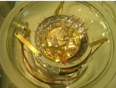
Investigation of structural lubricity on platinum nanoparticles under ambient conditions
Tam metin
Şekil
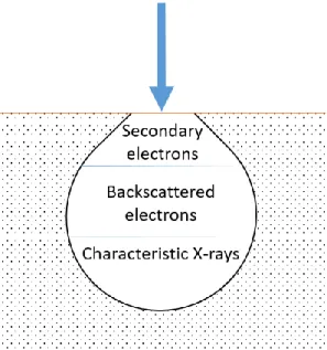
![Figure 2.1 Schematic of a scanning electron microscope. Taken from [35].](https://thumb-eu.123doks.com/thumbv2/9libnet/5844500.119819/25.892.173.781.405.774/figure-schematic-scanning-electron-microscope-taken.webp)
Benzer Belgeler
In this work, we are interested in performance investigation of different operation modes of IEEE 802.11af systems rather than solving the sparse channel estimation problem by
[r]
The objective of this study was to examine whether AP serotype 10-derived exotoxin, ApxI, caused apoptosis in porcine alveolar macrophages (PAMs) and to delineate the
ÜSTAD DOĞDUĞU GÜN TO PRAĞ A VERİLD İ Cenaze törenine katılan bin lerce kişi 26 Mayıs 1905’de do ğan ve İlâhi bir tesadüf eseri yi ne bir 26 Mayıs
To test if the information contained in these ChIPtigs is enough to recover the correct motifs, and if the rank- ings we are using help in such goal we next used our ranked ChIPtig
The conversion of surface methoxides (that are formed upon DME adsorption at 573 K on the alumina surface) to formates occur after the addition of NO 2 through the following
This interdisciplinary study has several theoretical and practical results for both.. study shows that foreign policy orientation of key decision makers can be captured with not
To investigate the optimum parameters for silica coating of quantum dots, the formation process of silica nanoparticles has been examined for different residence times and flow
