Magnetic Heterostructures of Transition Metal Dichalcogenides:
Antiparallel Magnetic Moments and Half-Metallic State
Mehmet Aras, Çetin Kılıç,
*
and Salim Ciraci
*
Cite This:J. Phys. Chem. C 2020, 124, 23352−23360
ACCESS
Metrics & More Article RecommendationsABSTRACT: Various forms of periodic, lateral, and vertical heterostructures constructed from magnetic transition metal dichalcogenide monolayers, FeTe2and NiTe2, have been investigated by using hybrid density functional
calculations. The lateral heterostructures formed from the stripes of these constituents joined along their armchair edges are found to be half-metallic within both constituent stripes with integer number of total magnetic moment per cell; they are semiconductor for spin-down electrons but metallic for spin-up ones. Additionally, the indirect band gap of these half-metallic structures in the energy range of visible light as well as their normal band lineup exhibit features that can be tunable with the width of stripes. Normal band lineup can lead to the confinement of excess spin-down
electrons and eventually to the change of dimensionality from two to one. Strong variations of the band gap can be attained by δ-doping. Half-metallicity spreads from the FeTe2side of the junction to the adjacent NiTe2side, which is metallic when stand-alone,
through strong Fe−Te−Ni bonds at the boundary. In contrast, in the thin, vertical heterostructures, where the interlayer coupling is rather weak, the half-metallic character is retained only in the FeTe2side; the NiTe2side remains a spin-polarized metal. Hence,
these vertical heterostructures form a semiconductor/metal junction with a Schottky barrier for one spin direction to function as a diode but a metal/metal junction for the opposite spin direction to function as a conductor. These lateral and vertical heterostructures have inhomogeneous magnetic moment configurations due to p−d hybridization; in both sides of the junction, chalcogen atoms have magnetic moments antiparallel to those at transition metal atoms. Functionalities revealed here are rare and can lead to crucial applications.
■
INTRODUCTIONExploiting unusual electronic structures of junctions or heterostructures and realizing diverse operation properties in crystals or slabs have been one of the prime activities in device physics and materials science since the 1980s. Initially, unusual quantization of electrons unveiled in 2D electrons confined in these junctions has led to the discovery of integer and fractional quantum Hall effects.1
Later, semiconductor/semi-conductor junctions brought about a number of interesting phenomena, such as normal, eclipsed, and staggered band lineups and single or multiple quantum well structure generated thereof, quantum size effects, etc.2,3
The formation of a Schottky barrier and the realization of diode function have been intensively explored in semiconductor/metal junctions.4,5 Recently, the realization of similar effects in the strictly 2D monolayers through in-plane lateral and vertical heterostruc-tures as well as width modulated nanoribbons have been the subject of several recent theoretical and experimental studies.6−8 It has been shown that (in-plane) lateral heterostructures with large alternation of constituents realized from the stripes of strictly 2D monolayers give rise to a wide range of features and functionalities. These are 2D metallic or narrow band gap semiconducting compounds, narrow 1D
metallic interconnects or nanowires in a wide 2D semi-conductor sheet, tunneling barriers and resonant tunneling double barrier structures, nanocapacitors, single and periodic metal/semiconductor junctions forming the Schottky barrier, etc.; see refs9,10and references therein.
While experimental and theoretical research on the monolayer and multilayer transition metal dichalcogenides (TMD) are continuously growing, the realization of vertical van der Waals solids11,12 as well as lateral, in-plane heterostructures13−16 of TMD monolayers brought about new ideas for novel devices.17−24 Vertical and lateral semiconductor/semiconductor junctions were considered as p−n diodes,25−38
photodiodes,33,34photodetectors,29,31,39solar cells,40 and electron-driven nanomanipulation.41 Owing to recent observations of magnetic order in two-dimensional
Received: July 28, 2020 Revised: September 28, 2020 Published: September 29, 2020
magnetic (FeTe2) stripe, the resulting composite structure was
found to exhibit the spin-valve effect. In fact, spintronic applications with 2D TMDs have been discussed in a number of recent papers, e.g., refs48,49. Furthermore, the formation of a tunable and linear Schottky barrier or the construction of a strictly 1D nanowires in a 2D semiconducting sheet through a δ-doping was deduced. Meanwhile, a most recent theoretical study50 based on density functional theory (DFT) using various approximations for the electron−electron interaction has revealed an inhomogeneous magnetic ground state in a number of TMD monolayers. In particular, it was found that the chalcogen atoms in the FeTe2and NiTe2monolayers have
magnetic moments antiparallel to that of the transition metal atoms, which is reminiscent of ferrimagnetic order. Com-parative analysis of the results of semilocal and hybrid DFT calculations, performed within the local density approximation (LDA) with the Ceperley−Alder functional51
or the generalized gradient approximation with the Perdew−Burke− Ernzerhof (PBE) functional52 with and without Hubbard U correction for on-site Coulomb interaction53 and using the Heyd−Scuseria−Ernzerhof (HSE) functional,54,55
respectively, has shown that hybrid-functional calculations rather than semilocal density-functional calculations yield a reliable prediction of the magnetic ground state of specific TMD monolayers.50
In view of these recentfindings, we carried out the present study to investigate the electronic and magnetic properties of the periodic, lateral, i.e., A:(FeTe2)p/(NiTe2)qand vertical, i.e.,
V:(FeTe2)p/(NiTe2)q, heterostructures (where p and q denote
the number of formula units of FeTe2and NiTe2in the unit
cell, respectively) by performing hybrid-functional (HSE) calculations, using the correct magnetic ground state of constituent TMD monolayers. Our study unveils the following important features of the foregoing heterostructures: (i) The lateral heterostructures combine both semiconductor/semi-conductor and metal/metal junctions for different spin directions, where the half-metallic character can be retained throughout the heterostructure. When the constituent stripes are narrow, the indirect band gap of spin-down electrons varies strongly with their widths of stripes, but it becomes uniform throughout the structure and hence attains the same value at either side of the junction. Electronically, these structures are considered to be single compound materials even if they are made by alternatingly different constituent TMD monolayers and are unanimously specified as heterostructures. However, when the constituent stripes become wider, the band gap differ at either side of the junction and their normal band lineup and resulting band offsets vary with the widths of constituent stripes. Accordingly, these predictions report a half-metallic heterostructure; the band offsets of its spin-down electrons are tunable with the widths of constituents. (ii) In the vertical heterostructures, one side of the junction is half-metallic, while
structures, we performed spin-polarized hybrid and semilocal DFT calculations by using the Vienna ab initio simulation package56(VASP) together with its projected-augmented-wave (PAW) potential database.57 The hybrid DFT calculations were carried out with the Heyd−Scuseria−Ernzerhof (HSE) functional.54,55 The semilocal calculations were performed within either the local density approximation using the Ceperley−Alder functional51
or the generalized gradient approximation using the Perdew−Burke−Ernzerhof (PBE) functional52 in combination with the D3 dispersion correc-tion.58 Hence, the van der Waals interaction is taken into account through the PBE-D3 scheme. The states in the electron configurations 3d74s1, 3d94s1, and 5s25p4 for iron,
nickel, and tellurium, respectively, were treated as valence states. The electronic wave functions were expanded into a plane-wave basis set with a cutoff energy of 400 eV. The vertical (lateral) heterostructures were modeled using suitable supercell geometries (with a vacuum spacing of 20 Å between periodic images of the monolayer along the direction perpendicular to the monolayer).
We performed structural optimizations where the equili-brium value of the 2D lattice constants as well as the lattice constant in the direction perpendicular to the layers were determined via minimization of the total energy, and the ionic positions were relaxed until the residual forces on atoms were reduced to be smaller than 10−2eV/Å. In order to analyze the stability of the optimized heterostructures, we computed their bond-length strainε distribution with respect to the respective bond lengths in bare FeTe2 and NiTe2 monolayers. The
Brillouin zone sampling was carried out using 12 × 8 × 1 (lateral heterostructure with p = q = 1), 8 × 8 × 1 (lateral heterostructures with p + q = 4), 4 × 8 × 1 (lateral heterostructures with p + q > 4), 12 × 12 × 4 (vertical heterostructure with p = q = 1), and 12× 12 × 2 (vertical heterostructure with p = q = 2) k-point meshes generated according to the Monkhorst−Pack scheme.59
Using the optimized structures, we performed self-consistent field electronic structure calculations in order to obtain the magnetic and electronic states of A:(FeTe2)p/(NiTe2)q and
V:(FeTe2)p/(NiTe2)q systems with various combination of p
and q. The atomic (μFe, μNi, and μTe) spin moments were
computed by dividing the total spin momentμtotamongst Fe,
Ni, and Te atoms according to the density-derived electrostatic and chemical (DDEC) spin partitioning technique.60,61 Throughout this paper, the total and atomic spin moments are given in units of Bohr magneton μB per cell and atom,
respectively.
■
RESULTSFeTe2 and NiTe2 Monolayers. Before focusing on the
lateral and vertical (FeTe2)p/(NiTe2)q heterostructures, we
free-standing FeTe2and NiTe2monolayers. Previous studies,
e.g., refs 9, 62, have shown that both FeTe2 and NiTe2
monolayers are stable in both H- and T-structures. The energy difference EH− ETbetween the H- and T-phases is calculated,
using HSE, to be−65 and 334 meV per formula unit for the FeTe2and NiTe2monolayers, respectively. Indeed, regardless
of the level of approximation in DFT,9the H- and T-structure has a lower energy for the FeTe2 and NiTe2 monolayers,
respectively. On the other hand, the occurrence of stable, higher-energy phases in heterostructures cannot be precluded since the lattice matching and commensurability at interfaces are favored in the course of heterostructure growth. Accordingly, we believe that NiTe2 can be grown in the
H-phase at the armchair edge of FeTe2 nanoribbons. For this
reason, in this paper, we place emphasis on the hetero-structures A:(FeTe2)p/(NiTe2)q with both constituent stripes
in the H structure.
Based on the results of LDA calculations, ferromagnetic and nonmagnetic ground states were assigned to the FeTe2 and
NiTe2monolayers, respectively, in earlier studies.9,62Recently,
however, a comparative analysis of the results obtained atfive levels of approximations50 revealed that the true magnetic ground state of FeTe2 and NiTe2 monolayers comprises
inhomogeneous magnetic moment configurations, and the chalcogen atoms by themselves have significant, antiparallel magnetic moments owing to the spin polarization of chalcogen atoms through p−d hybridization. Furthermore, the FeTe2
monolayer in the H structure, which is a half metal, has an integer magnetic moment ofμtot= 2; the magnetic moments
on Fe and Te atoms beingμFe= 3.10 andμTe=−0.55. On the
other hand, NiTe2 is a magnetic metal with a non-integer
magnetic moment ofμtot= 0.36; the magnetic moments on Ni
and Te atoms beingμNi= 0.60 andμTe=−0.12.
As for the electronic structure, the majority spin bands of the H-FeTe2monolayer, which are derived from the Te px+ pyand
Fe dx2− y2+ dxyand dxz+ dyzorbitals, cross the Fermi level and
hence display a metallic character. In contrast, an indirect band gap of 1.77 eV is opened up between the minority spin bands constructed from the states of the valence band maximum at the Γ-point derived from the Fe dxz + dyz and Te px + py
orbitals and the states of the conduction band minimum at the K-point derived from the Fe dx2− y2+ dxyand dz2, and Te px+
pyorbitals. These render the free-standing H-FeTe2monolayer
to be a half metal. On the other hand, both majority and minority spin bands of the NiTe2monolayer cross the Fermi
level, rendering it a magnetic metal with a small magnetic moment.
Lateral Heterostructures. We performed calculations for periodic, lateral heterostructures with armchair boundary, i.e., A:(FeTe2)p/(NiTe2)qwith (p, q) = (1,1), (1,3), (2,2), (3,1),
(3,3), (4,4), (5,5), constructed by joining armchair nanorib-bons of FeTe2 and NiTe2 (with p and q formula units of
constituents in their unit cells, respectively) commensurately. The results of these calculations are exemplified inFigures 1
and2.Figure 1a displays the optimized atomic structure of A: (FeTe2)5/(NiTe2)5, where the bond-length strain distribution
is indicated by coloring of the sticks representing the Fe−Te and Ni−Te bonds. The isosurfaces of spin densities and atomic magnetic moments of this heterostructure are shown inFigure 1b, which reveal an inhomogeneous magnetic moment configuration owing to antiparallel (mostly parallel) arrange-ment of the Fe (Ni) and Te moarrange-ments in the FeTe2(NiTe2)
stripe. The total magnetic moments of the FeTe2and NiTe2
stripes are +11.8μB and −1.8μB, respectively, indicating an
antiparallel alignment of the magnetic moments of these two constituent stripes. Remarkably, the total magnetic moment of A:(FeTe2)5/(NiTe2)5 have an integer value of μtot = 10μB,
which is indicative of half-metallic behavior (cf. refs 63, 64). The half-metallicity of this heterostructure is also deduced from the total and local densities of states (LDOS) presented
Figure 1.(a) Top and side views of the optimized atomic structure of lateral heterostructure A:(FeTe2)5/(NiTe2)5. The blue, green, and red balls
represent the Fe, Ni, and Te atoms, respectively. The sticks representing the Fe−Te and Ni−Te bonds are colored to indicate the bond-length strainε distribution, computed with respect to the bond lengths in the bare FeTe2and NiTe2monolayers. The subcells containing one formula unit
are specified by encircled numerals. (b) Isosurfaces of spin density ρs(r) and atomic magnetic moments (in units of Bohr magneton). The algebraic
sum of atomic magnetic moments in the FeTe2and NiTe2stripes are +11.8μBand−1.8μB, respectively. (c) Spin-polarized local density of states
(LDOS) for subcells③ and ⑧ and total density of states (DOS). (d) Energy diagram showing the spatial variation of the spin-down conduction and valence band edge energies. The Fermi level is indicated by the dotted-dashed line. (e) Change in the electronic chargeΔN at each subcell with respect to the free-standing FeTe2and NiTe2monolayers.
inFigure 1c.Figure 1d shows the spatial variation of the band edge energies obtained from LDOS values. The transitions of the conduction and valence band edges occur rather sharp at the junction, and hence from the electronics point of view, the heterostructure character is realized. The band gap of the NiTe2side is significantly smaller than that of the FeTe2side,
showing that A:(FeTe2)5/(NiTe2)5 is a type-I, or
straddling-gap, heterojunction. The occurrence of type-I band alignment can be traced to the close values of the work functionϕ for the bare FeTe2 (ϕ = 4.12 eV) and NiTe2 (ϕ = 4.15 eV)
monolayers, which is attributable to the similar electro-negativities of the Fe and Ni atoms.65 This is supported by the fact that the charge transfer at the interface between the FeTe2and NiTe2stripes, as well as the change in the electronic
charge ΔN throughout the heterostructure, remain small, as shown inFigure 1e, which means that strong interface dipoles do not form.
In order to see if the half-metallic behavior continues to exist when p ≠ q, we also discuss our results for A:(FeTe2)3/
(NiTe2)1, i.e., (p, q) = (3,1), and A:(FeTe2)1/(NiTe2)3, i.e., (p,
q) = (1,3), heterostructures summarized inFigure 2. Owing to the fact that one of the constituents in the unit cell has a very narrow width, these structures can be considered as the δ-doping of the wide constituent by the narrow one. For example, we can consider A:(FeTe2)3/(NiTe2)1as if the FeTe2
monolayer is δ-doped by one formula unit, narrow stripe NiTe2in every other, three-formula unit wide FeTe2host. The
moments and inhomogeneous magnetic moment configura-tions characterized by parallel alignment of the Fe and Ni moments and antiparallel alignment of the Te moments.
As exemplified in the preceding two paragraphs, the results obtained for various values of p and q indicate that all A: (FeTe2)p/(NiTe2)qstructures considered in this study exhibit
a half-metallic behavior associated with an integer total magnetic moment. It is interesting to note that, for these A: (FeTe2)p/(NiTe2)p structures, the total magnetic moment is
given byμtot= 2pμB. This indicates that the average magnetic
momentμ̅ = μtot/p = 2μBremains constant, i.e., independent of
the width of the constituent nanoribbons.
In Figure 3, we present the total and average magnetic moments of A:(FeTe2)p/(NiTe2)p, obtained from the LDA,
PBE+D3, and HSE calculations, in order to analyze how the predicted values ofμtotandμ̅ depend on the treatment of the
electron−electron interaction. It is seen that the predictions using LDA have an irregular trend for the variations ofμtotand
μ̅ with p. While the structures with p = 1,3,5,8 are nonmagnetic, those with p = 2,4,6,7,9,10 have nonzero magnetic moments. It is also clear that the LDA and PBE +D3 calculations for the same structures result in quite different magnetic moments. In contrast, the PBE+D3 and HSE results exhibit quite similar trends. Nonetheless, the calculations using PBE+D3 predict non-integer magnetic moments, which is at odds with the HSE results. This latter disagreement between PBE+D3 and HSE calculations can be attributed to the erroneous closure of the spin-down band gap of the FeTe2 monolayer in the PBE calculations, which
originates from the improper description of strong correlations of localized d electrons with a semilocal exchange-correlation functional, leading to fractional magnetic moments.50 The integer values of μtot and μ̅ are obtained for the correct
electronic ground state when the strong correlations are to
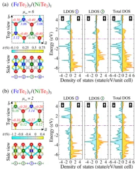
Figure 2. Atomic and electronic structures of (a) A:(FeTe2)3/
(NiTe2)1 and (b) A:(FeTe2)1/(NiTe2)3 heterostructures
(com-pounds). The spin-polarized total density of states (DOS) and local density of states (LDOS) for subcells① and ③ are plotted. The blue, green, and red balls represent the Fe, Ni, and Te atoms, respectively, next to which the atomic magnetic moments (in units of Bohr magneton) are given as italic numbers. Note that theμtotvalues equal
the algebraic sum of atomic magnetic moments. The sticks representing the Fe−Te and Ni−Te bonds are colored to indicate the bond-length strainε distribution, computed with respect to the bond lengths in the bare FeTe2and NiTe2monolayers. Since these
heterostructures display a uniform band gap throughout the unit cell, they are specified also as compounds.
Figure 3.Variation of the (a) total magnetic momentμtotin units of
Bohr magnetonμBper cell and (b) average magnetic momentμ̅ =
μtot/p of the lateral A:(FeTe2)p/(NiTe2)pstructures, obtained from
some extent taken into account by either adding a Hubbard U term to the PBE functional or using a hybrid functional. In view of this analysis, we assess that the hybrid rather than semilocal DFT calculations are more reliable in predicting the ground state of the magnetic TMD monolayers as well as their heterostructures.
The band edge energies for spin-down electrons in a variety of A:(FeTe2)p/(NiTe2)q structures and the FeTe2monolayer
(for comparison) are shown inFigure 4where the Fermi level is taken as the zero of band energy. In this figure, the band offsets are indicated by the red double-sided arrows. As pointed out in theIntroduction, the absence of band offsets for p, q≤ 3 is noteworthy. Electronically different domains in the heterostructure corresponding to the different constituent monolayers form only for p = q ≥ 4, as signified by the formation of a type-I band offset. In view of this feature, we designate A:(FeTe2)p/(NiTe2)q structures with p, q ≤ 3 as
compounds, as if a single material having the same repeating unit cell. On the other hand, the heterostructures with p = q≥ 4 can be viewed as a semiconductor/semiconductor junction with a type-I band offset for spin-down electrons but a metal/ metal junction for spin-up electrons.
It is seen inFigure 4that the spin-down band gaps of the A: (FeTe2)p/(NiTe2)q compounds are significantly smaller than
that of the FeTe2monolayer. This band gap, i.e., Eg↓, varies with
p and q: Eg↓ = 0.92 eV for p = q = 1, which increases
(decreases) to be 1.51 (0.51) eV when p (q) is increased to be 3 with q = 1 (p = 1). On the other hand, if p and q are both increased to be 2, the spin-down band gap becomes 1.06 eV. Further simultaneous increase of p and q to 3 increases the value of Eg↓to 1.16 eV, which is still considerably smaller than
the spin-down band gap of the bare FeTe2monolayer. It is also
clear fromFigure 4that the spin-down band gap of the FeTe2
(NiTe2) side in the A:(FeTe2)p/(NiTe2)p heterostructures
increases (decreases) as the constituent stripes get wider. Consequently, the difference between the band gaps of the FeTe2 and NiTe2 side increases as p gets larger, which is
associated by an increase in both conduction and valence band offsets.
In view of the above discussions, it is interesting to note that heterostructures with p = q ≥ 4 can form periodic multiple quantum well structures. Excess spin-down electrons through doping of the FeTe2stripe can be confined at the NiTe2stripe.
They can form 1D or quasi-1D spin-down electron system, which can move in the quantum well along NiTe2stripes. This
is an important outcome of these heterostructures that, from
2D electrons of either monolayer, one can realize/isolate 1D electrons with well-defined spin direction. Notably, in earlier bulk AlAs/GaAs heterostructures, 2D spin-unpolarized elec-trons were confined in the wells of GaAs.66
Even though we were unable to carry out HSE calculations for larger p = q, it appears that the band gap of spin-down electrons, which attributes a half-metallic character to the whole heterostructure, ceases at the NiTe2 side for higher
values of q. Under these circumstances, one expects that the heterostructures considered here can change to a half-metal/ metal junction for large q. This behavior as well as the band gaps of δ-doped heterostructures suggest that the metallic character of NiTe2 constituent can dominate the electronic
structure gradually with the increasing width of its stripe. Here, we demonstrate that, for 3 < p = q≤ 5, both sides of junctions are half-metallic with different band gaps. Now, in this prediction, an interesting question worth addressing is how the half-metallic behavior is maintained throughout the whole heterostructure despite the fact that one of their constituents, NiTe2, is a metal when free-standing. We believe that strong
Fe−Te−Ni bonds at the sharp armchair boundary between adjacent FeTe2and NiTe2stripes facilitate the spread of
half-metallicity into NiTe2stripes of narrow widths. This feature
can be utilized to design spintronic devices with tunable band gap corresponding to a given spin direction.
Vertical Heterostructures. The vertical heterostructures are constructed by the vertical stacking of FeTe2 and NiTe2
monolayers, which are kept by the weak van der Waals (vdW) attraction. In an earlier study,50we have demonstrated that the half-metallic behavior of the FeTe2 monolayer continues to
occur in its bilayer, but it is destroyed in trilayers and thicker multilayers. In the present paper, we consider periodically repeating V:(FeTe2)p/(NiTe2)q vertical heterostructures for p
= q = 1,2. Optimized atomic structures, atomic magnetic moments, LDOS at selected layers, and total DOS, obtained from the HSE calculations, are presented inFigure 5.
The minimum energy stacking sequence, where metal atoms (Fe or Ni) resides on top of chalcogen atoms to form hexagons in the top view, is determined by structure optimization. The average binding energy per constituent layer is found to be Eb
= 86 meV per layer per formula unit. Because of weak vdW coupling, the interlayer distance is large and prevents constituent layers from strong coupling. As a result, in the vertical heterostructure the constituent layers in the stack retain their electronic and magnetic properties to a large extent. In this respect, while the FeTe2layers in the vertical Figure 4.Band edge energies for spin-down electrons in the FeTe2monolayer and in a variety of A:(FeTe2)p/(NiTe2)qheterostructures. The Fermi
level is indicated by the dashed line, which is taken as the zero of band energy. The spin-down band gap (Eg↓) values in the FeTe2(blue) and NiTe2
(green) are given by blue and green arrows, respectively. Periodic heterostructures having the same Eg↓value in both sides of the junction are
heterostructures with p = q ≤ 2 remain half-metal with semiconducting spin-down electrons and metallic spin-up electrons, the NiTe2layers are metallic for both spin directions.
The TMD monolayers at either side of the junctions (1/1) and (2/2) are found to have antiparallel magnetic moments at different constituent atoms; the total magnetic moments per unit cell are calculated to be 2.35 and 4.70μB, respectively.
Accordingly, both heterostructures consist of a periodic semiconductor/metal junction for spin-down electrons and a metal/metal junction for spin-up electrons. The band gap at the semiconducting FeTe2 layer is deduced from LDOS
calculations to be Eg↓= 1.27 eV for p = q = 2. Even though the
width of this semiconducting side is thin, we nevertheless estimate the Schottky barrier energy for the spin-up electrons to be ES= 1.09 eV.
■
DISCUSSION AND CONCLUSIONSIn view of these results obtained from state-of-the art, first-principles calculations, we now discuss the crucial and novel features of magnetic heterostructures with underlying physics. As we pointed out, these features hold a great promise for future device applications:
correct magnetic state of the heterostructure under study. Our results demonstrate that the HSE method is suitable for this purpose.
(ii) Another critical feature unveiled in this study is the hybridization between p−d orbitals of chalcogen and transition metal atoms in the TMD heterostructure and resulting non-uniform/antiparallel distribution of mag-netic moments in A:(FeTe2)p/(NiTe2)q, which has been
skipped in earlier studies. As seen in this study, small but antiparallel magnetic moments on chalcogen atoms are decisive for the correct description of the magnetic ground state of the heterostructure.
(iii) The energy band gap and band offset variations with (p/ q) combination depicted inFigure 4involve interesting physical phenomena and herald potential applications thereof. Even though an in-plane heterostructure is constituted from two TMD stripes, one being half-metal and the other metal like A:(FeTe2)p/(NiTe2)q, it can
attain the half-metallic ground state all the way across the device. Close proximity maintained by strong Fe− Te−Ni bonds at the boundary between two constituents is the cause of the transfer or spread of the half-metallic state from the FeTe2 side to the otherwise metallic
NiTe2side. A noteworthy situation is that the band gaps
of spin-down electrons are uniform across the unit cell for p and q≤ 3 (but strongly dependent on their values), as if a single crystal, but differ abruptly when p = q > 3. Accordingly, a non-uniform band diagram in direct space with a sharp, normal band alignment occurs at the junction as shown inFigure 1. This is the manifestation of the formation of electronically different zones at both sides of the junction. It should be noted that, in contrast to in-plane, lateral heterostructures, the spread of half-metallic character from the FeTe2side to the NiTe2side
cannot be realized in the absence of strong Fe−Te−Ni bonds between layers at the junction.
(iv) The band gap of the NiTe2side being smaller than that
of the FeTe2 side and also further decreasing with
increasing q constitutes a 1D multiple quantum well structure. The depth of this well or the energy barrier to the FeTe2 side increases with increasing q. Upon the
modulation doping of the FeTe2 side, the excess
spin-down electrons flowing into 1D quantum well and occupying well-defined quantum well states can become confined. The formation of the confined states and their level splitting can be deduced from the effective mass theory.67This way, 2D itinerant electrons of the in-plane heterostructure undergo a 2D → 1D change in dimensionality, and they become confined to the NiTe2 side. These electrons can transport spin and
charge only along the armchair edge in NiTe2in
well-defined conduction channels. Owing to the modulation
Figure 5.Atomic and electronic structures of vertical heterostructures (a) V:(FeTe2)1/(NiTe2)1and (b) V:(FeTe2)2/(NiTe2)2. Left: Side
views of atomic structures. The blue, green, and red balls represent the Fe, Ni, and Te atoms, respectively. The sticks representing the Fe−Te and Ni−Te bonds are colored to indicate the bond-length strainε distribution, computed with respect to the bond lengths in the bare FeTe2and NiTe2monolayers. Numerals in circles identify the
layers. Middle: The atomic (μFe,μNi, andμTe) magnetic moments in
units of Bohr magneton. The magnetic moments at transition metal and chalcogen atoms are aligned antiparallel as long asμFe,μNi>0 and
μTe<0. Right: Density of states projected to the specific layers
indicated by numerals (LDOS) and total density of states (Total DOS).
doping68in the FeTe2side, the impurity scattering in the
NiTe2side is minimized and the phase breaking length is
maximized. The energy level splitting of these channels change with the band offset or the energy barrier (height) between the conduction band edges of FeTe2
and NiTe2and hence with q. Accordingly, the barrier
height provides a means of tunability for 1D quantum conduction.
(v) On can deduce interesting devices from the normal band lineup discussed above. For example, the (FeTe2)p/
(NiTe2)q/(FeTe2)p structure with p and q > 3
commensurately joined to two wide stripes of NiTe2
from both (FeTe2)p ends can form a double barrier
resonant tunneling device.3 While both wide NiTe2
stripes capping (FeTe2)p from their free ends are
metallic, (NiTe2)q in between is half-metallic, narrow
band semiconductor and forms localized (confined) states for spin-down electrons. The metallic electron in the wide NiTe2side at the left can tunnel through these
confined states to the other wide NiTe2side at the right
when energies are matched. The confined states at the middle part of the device act as a spin-filter. It is known that the tunneling across two FeTe2 barriers through
these confined states occur in a very short time when the energies are matched. The operation parameters of this device can be monitored by the width of NiTe2between
FeTe2barriers.
(vi) Heterostructures can be constructed not only from very long stripes of constituents as in the present study but also fromfinite size stripes or from nanoribbons.6,8The width (parallel to boundary) and length (perpendicular to the boundary) of nanoribbons and the type of edge termination are available parameters to monitor the physical properties of the device. Carriers in hetero-structures formed from nanoribbons are quasi-1D along the axis of the nanoribbon. The quantum well formation and resulting confinement in one of the constituents lead to the change of dimensionality from 1D to 0D (namely, quantum dots).
(vii) The antiparallel alignment of local magnetic moments at constituent elements constructed through the spin polarization at chalcogen atoms as a result of p−d orbital hybridization and hence the negative exchange coupling between transition metal and chalcogen atoms may facilitate the spin transfer in these heterostructures. (viii) An important question to be addressed is whether these magnetic heterostructures with all their interesting properties are stable or not. Stability becomes even a more critical issue for lateral, in-plane heterostructures since the bonds at the junction region may be subjected to severe strain or deformation. This issue can be analyzed by using the bond-length strain distributions presented inFigures 1,2, and5. As seen inFigures 1and
2, the bond strains in A:(FeTe2)p/(NiTe2)q
hetero-structures are rather low and varies within a narrow range−1.2% < ε < +0.9%. The bond strains in vertical vdW heterostructures inFigure 5are even smaller in the absence of bonds between TMD layers. In our previous paper,9we demonstrated the thermal stability of in-plane (MoTe2)p/(NiTe2)q heterostructures, which have
sig-nificantly higher values of bond strain in a much wider range−6.2% < ε < +7.4% owing to low commensur-ability, by performing ab initio molecular dynamics
simulations at a temperature considerably higher than room temperature. As long as (FeTe2)p/(NiTe2)q
heterostructures have significantly smaller bond strains in comparison to thermally stable (MoTe2)p/(NiTe2)q
heterostructures, we find it unlikely that the magnetic heterostructures studied in the present paper become prone to thermal instability at moderate temperatures. In conclusion, in this paper, we considered lateral and vertical heterostructures composed of FeTe2 and NiTe2
monolayers using the HSE method, which allowed us to predict the correct magnetic ground state for these stand-alone monolayers. The armchair edged heterostructures with p = q = 1− 5 , as well as δ-doping realized thereof are found to be half-metallic with integer magnetic moment per cell. Namely, all these structures were semiconductor for spin-down electrons, but metallic for spin-up electrons. Due to different band gaps that occurred in different and wide TMD stripes, normal band-lineups are deduced. Additionally, the indirect band gap of these half-metallic structures exhibits an excellent tunability with the width of the constituent stripes. Strong variations of the band gap can be attained byδ-doping. The appearance of half-metallic behavior in the whole material for a limited range of alternation of constituents is found to be a rare. The spread of half-metallicity from one (FeTe2) to the other (NiTe2) side,
which is metallic when stand-alone, is attributed to the strong Fe−Te−Ni bonds at the sharp boundary. While the electrons in the periodic A:(FeTe2)p/(NiTe2)q with p, q≤ 3 is
two-dimensional (2D), excess spin-down electrons in hetero-structures with p = q > 3 may change their dimensionality from 2D to 1D through the quantum confinement in the quantum wells at the NiTe2 stripe. The quantization (that is different
from 2D) and the quantum conductance of these 1D, spin-down electrons can be of fundamental and technological interest, and should be experimentally observable.
In contrast to lateral heterostructures, the half-metallic character can be retained only in the FeTe2side in the thin,
vertical heterostructures. While the FeTe2side has a band gap
for spin-down electrons, the NiTe2side is metallic for the same
spin direction. However, both sides are metallic for the spin-up electrons. Accordingly, the vertical heterostructure forms a semiconductor/metal junction with a Schottky barrier for one spin direction but a metal/metal junction for the opposite spin direction. Hence, such a system shall function as a diode for one spin direction and a conductor for the opposite spin direction. In the present study, we estimated the Schottky barrier energy for a single spin direction. Interestingly, the inhomogeneous magnetic order with antiparallel magnetic moments at constituent atoms is also retained for thin alternation of constituents. This functionality is rather rare in vertical, van der Waals heterostructures and can promise crucial spintronic applications.
Finally, we hope that the importance of the proper treatment of electron−electron interaction in magnetic TMD hetero-structures as revealed in this study will guide similar future studies concerning magnetic 2D heterostructures.
■
AUTHOR INFORMATIONCorresponding Authors
Çetin Kılıç − Department of Physics, Gebze Technical University, 41400 Kocaeli, Turkey; orcid.org/0000-0003-2690-4940; Email:[email protected]
The authors declare no competingfinancial interest.
■
ACKNOWLEDGMENTSThe numerical calculations reported here were carried out at the High Performance and Grid Computing Center of TUBITAK ULAKBIM. S.C. acknowledges the financial support of Academy of Science of Turkey (TUBA).
■
REFERENCES(1) Ando, T.; Fowler, A. B.; Stern, F. Elec-tronic Properties of Two-Dimensional Sys-tems. Rev. Mod. Phys. 1982, 54, 437−672.
(2) Tsu, R.; Esaki, L. Tunneling in a FiniteSuperlattice. Appl. Phys. Lett. 1973, 22, 562−564.
(3) Chang, L. L.; Esaki, L.; Tsu, R. ResonantTunneling in Semiconductor Double Barriers. Appl. Phys. Lett. 1974, 24, 593−595. (4) Schottky, W. Halbleitertheorie der Sperrschicht. Naturwissen-schaften 1973, 26, 843.
(5) Tersoff, J. Schottky Barrier Heights and the Continuum of Gap States. Phys. Rev.Lett. 1984, 52, 465−468.
(6) Topsakal, M.; Sevinçli, H.; Ciraci, S. Spin Confinement in the Superlattices of Graphene Ribbons. Appl. Phys. Lett. 2008, 92, 173118.
(7) Sevinçli, H.; Topsakal, M.; Ciraci, S. Superlattice structures of graphene-based armchair nanoribbons. Phys. Rev. B 2008, 78, 245402. (8) Şahin, H.; Cahangirov, S.; Topsakal, M.; Bekaroglu, E.; Akturk, E.; Senger, R. T.; Ciraci, S. Monolayer Honeycomb Structures of Group-IV Elements and III-V Binary Compounds: First-Principles Calculations. Phys. Rev. B 2009, 80, 155453.
(9) Aras, M.; Kılıç, Ç.; Ciraci, S. Planar Heterostructures of Single-Layer Transition Metal Dichalcogenides: Composite Structures, Schottky Junctions, Tunneling Barriers, and Half Metals. Phys. Rev. B 2017, 95, No. 075434.
(10) Aras, M.; Kılıç, Ç.; Ciraci, S. Lateral and Vertical Heterostructures of Transition Metal Dichalcogenides. J. Phys. Chem. C 2018, 122, 1547−1555.
(11) Geim, A. K.; Grigorieva, I. V. van der Waals Heterostructures. Nature 2013, 499, 419−425.
(12) Seo, D. M.; Lee, J.-H.; Lee, S.; Seo, J.; Park, C.; Nam, J.; Park, Y.; Jin, S.; Srivastava, S.; Kumar, M.; et al. Ultrafast Excitonic Behavior in Two-Dimensional Metal-Semiconductor Heterostructure. ACS Photonics 2019, 6, 1379−1386.
(13) Liu, Z.; Ma, L.; Shi, G.; Zhou, W.; Gong, Y.; Lei, S.; Yang, X.; Zhang, J.; Yu, J.; Hackenberg, K. P.; et al. In-Plane Heterostructures of Graphene and Hexagonal Boron Nitride with Controlled Domain Sizes. Nat. Nanotechnol. 2013, 8, 119−124.
(14) Hong, X.; Kim, J.; Shi, S.-F.; Zhang, Y.; Jin, C.; Sun, Y.; Tongay, S.; Wu, J.; Zhang, Y.; Wang, F. Ultrafast Charge Transfer in Atomically Thin MoS2/WS2 Heterostructures. Nat. Nanotechnol.
2014, 9, 682−686.
(15) Lim, H.; Yoon, S. I.; Kim, G.; Jang, A.-R.; Shin, H. S. Stacking of Two-Dimensional Materials in Lateral and Vertical Directions. Chem. Mater. 2014, 26, 4891−4903.
(16) Kobayashi, Y.; Yoshida, S.; Maruyama, M.; Mogi, H.; Murase, K.; Maniwa, Y.; Takeuchi, O.; Okada, S.; Shigekawa, H.; Miyata, Y. Continuous Heteroepitaxy of Two-Dimensional Heterostructures Based on Layered Chalcogenides. ACS Nano 2019, 13, 7527−7535.
Nanoribbon Lateral Heterostructure. Phys. Chem. Chem. Phys. 2017, 19, 1303−1310.
(21) Zhao, J.; Cheng, K.; Han, N.; Zhang, J. Growth Control, Interface Behavior, Band Alignment, and Potential Device Applica-tions of 2D Lateral Heterostructures. WIREs Comput. Mol. Sci. 2018, 8, e1353.
(22) Ávalos-Ovando, O.; Mastrogiuseppe, D.; Ulloa, S. E. Lateral Heterostructures and One-Dimensional Interfaces in 2D Transition Metal Dichalcogenides. J. Phys.:Condens. Matter 2019, 31, 213001.
(23) Liu, Y.; Zhang, S.; He, J.; Wang, Z. M.; Liu, Z. Recent Progress in the Fabrication, Properties, and Devices of Heterostructures Based on 2D Materials. Nano-MicroLett. 2019, 11, 13.
(24) Wang, J.; Li, Z.; Chen, H.; Deng, G.; Niu, X. Recent Advances in 2D Lateral Heterostructures. Nano-Micro Lett. 2019, 11, 48.
(25) Zhang, Z.; Chen, P.; Duan, X.; Zang, K.; Luo, J.; Duan, X. Robust Epitaxial Growth of Two-Dimensional Heterostructures, Multiheterostructures, and Superlattices. Science 2017, 357, 788−792. (26) Paul, A. K.; Kuiri, M.; Saha, D.; Chakraborty, B.; Mahapatra, S.; Sood, A. K.; Das, A. Photo-Tunable Transfer Characteristics in MoTe2−MoS2Vertical Heterostructure. NPJ 2D Mater Appl. 2017, 1,
17.
(27) Chiu, M.-H.; Li, M.-Y.; Zhang, W.; Hsu, W.-T.; Chang, W.-H.; Terrones, M.; Terrones, H.; Li, L.-J. Spectroscopic Signatures for Interlayer Coupling in MoS2−WSe2 van der Waals Stacking. ACS
Nano 2014, 8, 9649−9656.
(28) Gong, Y.; Lin, J.; Wang, X.; Shi, G.; Lei, S.; Lin, Z.; Zou, X.; Ye, G.; Vajtai, R.; Yakobson, B. I.; et al. Vertical and In-plane Heterostructures from WS2/MoS2 Mono-layers. Nat. Mater. 2014,
13, 1135−1142.
(29) Xue, Y.; Zhang, Y.; Liu, Y.; Liu, H.; Song, J.; Sophia, J.; Liu, J.; Xu, Z.; Xu, Q.; Wang, Z.; et al. Scalable Production of a Few-Layer MoS2/WS2 Vertical Heterojunction Array and Its Application for
Photodetectors. ACS Nano 2016, 10, 573−580.
(30) Chen, K.; Wan, X.; Wen, J.; Xie, W.; Kang, Z.; Zeng, X.; Chen, H.; Xu, J.-B. Electronic Properties of MoS2−WS2Heterostructures
Synthesized with Two-Step Lateral Epitaxial Strategy. ACS Nano 2015, 9, 9868−9876.
(31) Gong, Y.; Lei, S.; Ye, G.; Li, B.; He, Y.; Keyshar, K.; Zhang, X.; Wang, Q.; Lou, J.; Liu, Z.; et al. Step Growth of Two-Dimensional WSe2/MoSe2 Heterostructures. Nano Lett. 2015, 15,
6135−6141.
(32) Ross, J. S.; Rivera, P.; Schaibley, J.; Lee-Wong, E.; Yu, H.; Taniguchi, T.; Watan-abe, K.; Yan, J.; Mandrus, D.; Cobden, D.; et al. Interlayer Exciton Optoelectronics in a 2D Heterostructure p−n Junction. Nano Lett. 2017, 17, 638−643.
(33) Son, Y.; Li, M.-Y.; Cheng, C.-C.; Wei, K.-H.; Liu, P.; Wang, Q. H.; Li, L.-J.; Strano, M. S. Observation of Switchable Photo response of a Monolayer WSe2−MoS2 Lateral Heterostructure via
Photo-current Spectral Atomic Force Microscopic Imaging. Nano Lett. 2016, 16, 3571−3577.
(34) Duan, X.; Wang, C.; Shaw, J. C.; Cheng, R.; Chen, Y.; Li, H.; Wu, X.; Tang, Y.; Zhang, Q.; Pan, A.; et al. Lat-eral Epitaxial Growth of Two-Dimensional Layered Semiconductor Heterojunctions. Nat. Nanotechnol. 2014, 9, 1024−1030.
(35) Li, H.; Li, P.; Huang, J.-K.; Li, M.-Y.; Yang, C.-W.; Shi, Y.; Zhang, X.-X.; Li, L.-J. Laterally Stitched Heterostructures of Transition Metal Dichalcogenide: Chemical Vapor Deposition
Growth on Litho-graphically Patterned Area. ACS Nano 2016, 10, 10516−10523.
(36) Chen, J.; Zhou, W.; Tang, W.; Tian, B.; Zhao, X.; Xu, H.; Liu, Y.; Geng, D.; Tan, S. J. R.; Fu, W.; et al. Lateral Epitaxy of Atomically Sharp WSe2/WS2 Hetero-junctions on Silicon Dioxide Substrates.
Chem. Mater. 2016, 28, 7194−7197.
(37) Yu, J. H.; Lee, H. R.; Hong, S. S.; Kong, D.; Lee, H.-W.; Wang, H.; Xiong, F.; Wang, S.; Cui, Y. Vertical Heterostructure of Two-Dimensional MoS2and WSe2with Vertically Aligned Layers. Nano
Lett. 2015, 15, 1031−1035.
(38) Li, M.-Y.; Shi, Y.; Cheng, C.-C.; Lu, L.-S.; Lin, Y.-C.; Tang, H.-L.; Tsai, M.-H.-L.; Chu, C.-W.; Wei, K.-H.; He, J.-H.; et al. Epitaxial Growth of a MonolayerWSe2−MoS2Lateral p−n Junction withan Atomically Sharp Interface. Science 2015, 349, 524−528.
(39) Yu, Y.; Hu, S.; Su, L.; Huang, L.; Liu, Y.; Jin, Z.; Purezky, A. A.; Geohe-gan, D. B.; Kim, K. W.; Zhang, Y. et al. Equally Efficient Interlayer Exciton Relaxation and Improved Absorption in Epitaxial and Nonepitaxial MoS2/WS2 Heterostructures. 2015, 15, 486−491,
DOI: 10.1021/nl5038177.
(40) Besse, R.; Lima, M. P.; Da Silva, J. L. F. First-Principles Exploration of Two-Dimensional Transition Metal Dichalcogenides Based on Fe, Co, Ni, and Cu Groups and Their van der Waals Heterostructures. ACS Appl. Energy Mater. 2019, 2, 8491−8501.
(41) Mendes, R. G.; Pang, J.; Bachmatiuk, A.; Ta, H. Q.; Zhao, L.; Gemming, T.; Fu, L.; Liu, Z.; Rümmeli, M. H. Electron-Driven In Situ Transmission Electron Microscopy of 2D Transition Metal Dichalcogenides and Their 2D Heterostructures. ACS Nano 2019, 13, 978−995.
(42) Du, J.; Xia, C.; Xiong, W.; Wang, T.; Jia, Y.; Li, J. Two-dimensional Transition-metal Dichalcogenides-based Ferromagnetic van der Waals Heterostructures. Nanoscale 2017, 9, 17585−17592.
(43) Piquemal-Banci, M.; Galceran, R.; Martin, M.-B.; Godel, F.; Anane, A.; Petroff, F.; Dlubak, B.; Seneor, P. 2D-MTJs: Introducing 2D Materials in Magnetic Tunnel Junctions. J. Phys. D: Appl. Phys. 2017, 50, 203002.
(44) Burch, K. S.; Mandrus, D.; Park, J.-G. Magnetism in Two-Dimensional van der Waals Materials. Nature 2018, 563, 47−52.
(45) Song, T.; Cai, X.; Tu, M. W.-Y.; Zhang, X.; Huang, B.; Wilson, N. P.; Seyler, K. L.; Zhu, L.; Taniguchi, T.; Watanabe, K.; et al. Giant Tunneling Magnetoresistance in Spin-Filter van der Waals Hetero-structures. Science 2018, 360, 1214−1218.
(46) Gibertini, M.; Koperski, M.; Morpurgo, A. F.; Novoselov, K. S. Magnetic 2D Materials and Heterostructures. Nat. Nanotechnol. 2019, 14, 408−419.
(47) Gong, C.; Zhang, X. Two-dimensional Magnetic Crystals and Emergent Heterostructure Devices. Science 2019, 363, eaav4450.
(48) Jin, C.; Solomon, G. C. Controlling Band Alignment in Molecular Junctions: Utilizing Two-Dimensional Transition-Metal Dichalcogenides as Electrodes for Thermoelectric Devices. J. Phys. Chem. C 2018, 122, 14233−14239.
(49) Wang, S.; Pratama, F. R.; Ukhtary, M. S.; Saito, R. Independent Degrees of Freedom in Two-dimensional Materials. Phys. Rev. B 2020, 101, No. 081414.
(50) Aras, M.; Kılıç, Ç.; Ciraci, S. Magnetic Ground State in FeTe2,
VS2, and NiTe2 Monolayers: Antiparallel Magnetic Moments at
Chalcogen Atoms. Phys. Rev. B 2020, 101, No. 054429.
(51) Ceperley, D. M.; Alder, B. J. Ground State of the Electron Gas by a Stochastic Method. Phys. Rev. Lett. 1980, 45, 566−569.
(52) Perdew, J. P.; Burke, K.; Ernzerhof, M. Generalized Gradient Approximation Made Simple. Phys. Rev. Lett. 1996, 77, 3865−3868.
(53) Dudarev, S. L.; Botton, G. A.; Savrasov, S. Y.; Humphreys, C. J.; Sutton, A. P. Electron-Energy-Loss Spectra and the Structural Stability of Nickel Oxide: An LSDA+U study. Phys. Rev. B 1998, 57, 1505− 1509.
(54) Heyd, J.; Scuseria, G. E.; Ernzerhof, M. Hybrid Functionals Based on a Screened Coulomb Potential. J. Chem. Phys. 2003, 118, 8207−8215.
(55) Krukau, A. V.; Vydrov, O. A.; Izmaylov, A. F.; Scuseria, G. E. Influence of the Exchange Screening Parameter on the Performance of Screened Hybrid Functionals. J. Chem. Phys. 2006, 125, 224106.
(56) Kresse, G.; Furthmüller, J. Efficient Iterative Schemes for ab initio Total-Energy Calculations Using a Plane-Wave Basis Set. Phys. Rev. B 1996, 54, 11169−11186.
(57) Kresse, G.; Joubert, D. From Ultra-soft Pseudopotentials to the Projector Augmented-Wave Method. Phys. Rev. B 1999, 59, 1758− 1775.
(58) Grimme, S.; Ehrlich, S.; Goerigk, L. Ef-fect of the Damping Function in Dispersion Corrected Density Functional Theory. J. Comput. Chem. 2011, 32, 1456−1465.
(59) Monkhorst, H. J.; Pack, J. D. Special Points for Brillouin-Zone Integrations. Phys. Rev. B 1976, 13, 5188−5192.
(60) Manz, T. A.; Sholl, D. S. Methods for Computing Accurate Atomic Spin Moments for Collinear and Noncollinear Magnetism in Periodic and Nonperiodic Materials. J. Chem. Theory Comput. 2011, 7, 4146−4164.
(61) Limas, N. G.; Manz, T. A. Introducing DDEC6 Atomic Population Analysis: Part 4. Efficient Parallel Computation of Net Atomic Charges, Atomic Spin Moments, Bond Orders, and More. RSC Adv. 2018, 8, 2678−2707.
(62) Ataca, C.; Şahin, H.; Ciraci, S. Stable, Single-Layer MoX2
Transition-Metal Oxides and Dichalcogenides in a Honeycomb-Like Structure. J. Phys. Chem. C 2012, 116, 8983−8999.
(63) Sato, K.; Bergqvist, L.; Kudrnovský, J.; Dederichs, P. H.; Eriksson, O.; Turek, I.; Sanyal, B.; Bouzerar, G.; Katayama-Yoshida, H.; Dinh, V. A.; et al. First-principles theory of dilute magnetic semi-conductors. Rev. Mod. Phys. 2010, 82, 1633−1690.
(64) Wang, S.; Yu, J. Magnetic Behaviors of 3d Transition Metal-Doped Silicane: a First-Principle Study. J. Supercond. Novel Magn. 2018, 31, 2789−2795.
(65) Pauling, L. The Nature of the Chemical Bond and the Structure of Molecules and Crystals: An Introduction to Modern Structural Chemistry; George Fisher Baker Non-Resident Lecture Series; Cornell University Press: Ithaca, New York,1960.
(66) Ciraci, S.; Batra, I. P. Self-consistent Study of Confined States in Thin GaAs-AlAs Superlattices. Phys. Rev. B 1987, 36, 1225−1232. (67) Mori, S.; Ando, T. Electronic Properties of a Heavily-doped n-typeGaAs−Ga1−xAlxAs Superlattice. Surf. Sci. 1980, 98, 101−107.
(68) Dingle, R.; Störmer, H. L.; Gossard, A. C.; Wiegmann, W. Electron Mobilities in Modulation-doped Semiconductor Hetero-junction Superlattices. Appl. Phys. Lett. 1978, 33, 665−667.