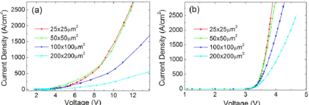
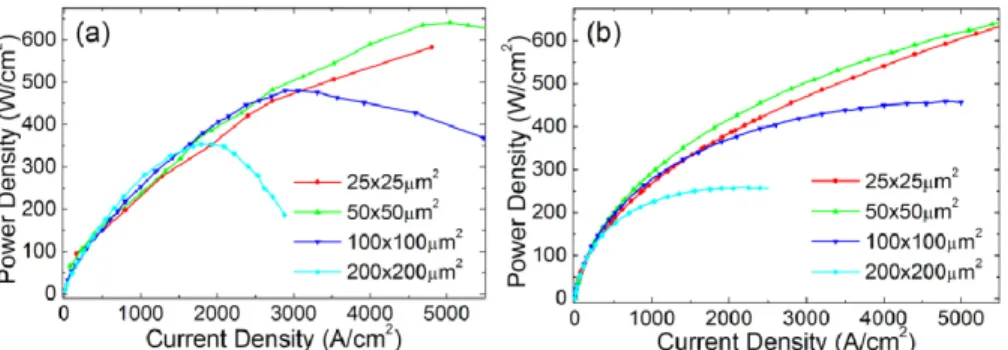
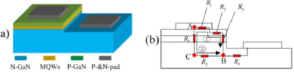
Low thermal-mass LEDs: Size effect and limits
Tam metin
Şekil
Benzer Belgeler
Overall mechanical results exhibited better tensile strength and modulus for the higher loading level (10 wt%) CF into LDPE, compared with that of lower loading levels of CF and
Stocking density for the intensive rearing of juvenile crayfish, Pacifastacus leniusculus (Astacidae), using Artemia nauplii to supplement a dry diet from the onset of
Göka’nın ikinci bö- lümde sorduğu soru, kadim medeniyetlerden beri insanlığın “Ben kimim?” sorusu kadar önemli ve merkezî bir soru: “Gitmek mi zor kalmak mı?”
Đşletmeyi Toplam Kalite Yönetimi ya da benzeri yeni yönetsel yaklaşımlarla yönetmeyi hedefleyen ve katılımcılığı yaşama geçirmeyi amaçlayan her yönetici kendi
With fixed clustering, full utilization of the CHs and selecting the sensor node with maximum residual energy, it can be observed that MESA provides a significant energy savings
However, this study suggests that by using other performance measures instead of preserving the use of ROA, the mechanism through which board independence affects firm
The purpose of this project is to investigate experimentally the tensile and flexural properties of polyethylene (PE), high density polyethylene (HDPE) and
the temperature distribution inside the tank 200 L scheme 2b represented in Figure 6.7 (c) show that thermal stratification was unstable and this due to heat losses to
