J- ' '' "' ·, >·^
§■ 'i' ■
w'i. л Г Т І и '{О T éC Ψ @7·2. • P SLOW-VOLTAGE CURRENT-MODE CMOS FILTER
STRUCTURE FOR HIGH FREQUENCY
APPLICATIONS
A THESIS
SUBMITTED TO THE DEPARTMENT OF ELECTRICAL AND ELECTRONICS ENGINEERING
AND THE INSTITUTE OF ENGINEERING AND SCIENCES OF BILKENT UNIVERSITY
IN PARTIAL FULFILLMENT OF THE REQUIREMENTS FOR THE DEGREE OF
MASTER OF SCIENCE
By
Aydın İlker Karşılayan July 1995
IkL язча. k z ^
■t 33 5
I certify that I have read this thesis and that in my opinion it is fully adequate, in scope and in quality, as a thesis for the degree of Master of Science.
Assodf Prof. Dr. Mehmet AlnTan(Supervisor)
I certify that I have read this thesis and that in my opinion it is fully adequate, in scope and in quality, as a thesis for the degree of Master of Science.
Prof. Dr. Abdullah Atalar
I certify that I have read this thesis and that in my opinion it is fully adequate, in scope and in quality, as a thesis for the degree of Master of Science.
Prof./lDr. Hayrettin Köymcn
Approved for the Institute of Engineering and Sciences:
Prof. Dr. Mehnjep/tiaray
Director of Institute of Engineering and Sciences
ABSTRACT
L O W -V O L T A G E C U R R E N T -M O D E C M O S F IL T E R S T R U C T U R E F O R H IG H F R E Q U E N C Y A P P L IC A T IO N S
A ydın İlker Karşılayan
M .S . in Electrical and Electronics Engineering Supervisor: Assoc. Prof. Dr. M ehm et A li Tan
July 1995
In this thesis, a new method for the design o f tunable current-mode CMOS filters is presented. The proposed structure is suitable for low-voltage (3V) and high frequency applications. Basic building blocks are differential damped integrator and differential damped differentiator, which have tunable com er fre quencies. Using first order building blocks and applying feedback techniques, biquadratic sections of low-pass, high-pass and band-pass filters are generated. Higher order filters are implemented by using cascaded biquad synthesis. Fil ters are tuned by means of two control voltages, from 50% to 130% o f their corner frequencies. HSPICE simulations show that filter implementation up to 0.5GHz is possible for 2.4^ CMOS technology. The available frequency range can be increased using a better technology such as 0.7/i CMOS. Layouts for two test chips are generated using CADENCE full-custom design environment for 0.7/i and 2.4/i CMOS processes.
Keywords : Filter, low-voltage, current-mode.
ÖZET
Y Ü K S E K F R E K A N S U Y G U L A M A L A R I İÇ İN D Ü Ş Ü K G E R İL İM L İ A K I M M O D U C M O S S Ü Z G E Ç Y A P IS I
Aydın İlker Karşılayan
Elektrik ve Elektronik Mühendisliği Bölüm ü Yüksek Lisans Tez Yöneticisi: Dr. M ehm et Ali Tan
Tem m uz 1995
Bu tezde, ayarlanabilir akım modu CMOS süzgeç tasarımı için yeni bir metod sunulmuştur. Önerilen yapı, düşük gerilim ve yüksek frekans uygulamaları için uygundur. Temel yapı blokları, köşe frekansları ayarlanabilen sönümlü fark integr«J alıcı ile sönümlü fark türev alıcıdır. Birinci derece yapı blok larını kullanarak ve geri besleme teknikleri uygulayarak, alçak-geçiren, yüksek- geçiren ve band-geçiren ikinci derece süzgeç blokları oluşturulmuştur. Daha yüksek dereceli süzgeçler, ikinci dereceden süzgeçlerin ardarda bağlanmcisı ile gerçekleştirilmiştir. Süzgeçler iki kontrol gerilimi yoluyla köşe frekanslarının %50’sinden %130’una kadar ayarlanabilmektedir. HSPICE simulasyonları göstermektedir ki, 2.4// CMOS teknolojisi ile O.bGHz'e kadar süzgeçlerin gerçekleştirilmesi mümkündür. Kullanılabilir frekans bandı, 0.7// gibi daha iyi bir teknoloji kullanılarak arttınlabilinir. CADENCE’m 0.7// ve 2.4// CMOS tasarım ortamları kullanılarak iki test yongasının yerleşim planlan üretilmiştir.
Anahtar Kelimeler : Süzgeç, düşük gerilim, akım modu.
ACKNOWLEDGEMENT
I would like to express my sincere gratitude to Dr. Mehmet Ali Tan for his supervision, guidance, suggestions and invaluable encouragement throughout the development of this thesis.
I would like to thank to Dr. Abdullah Atalar and Dr. Hayrettin Köymen for reading the manuscript and commenting on the thesis.
Special thanks are due to Ayhan Bozkurt, Suat Ekinci, Tolga Yalçın, Göksenin Yaralıoğlu and Oğan Ocalı for their encouragement and suggestions. I would like to express my appreciation to all Graduate Students in this de partment for their continuous support.
And finally, I would like to thank to my parents, whose understanding made this study possible.
TABLE OF CONTENTS
1 I N T R O D U C T I O N 1
2 B A S IC B U IL D IN G B L O C K S 4
2.1 Damped In te g ra to r... 11
2.2 Damped D ifferen tiator... 13
3 T U N I N G 16 3.1 D ow n -T u n in g ... 18 3.2 U p-Tuning... 22 4 I M P L E M E N T A T I O N O F F IL T E R B L O C K S 28 4.1 Low-pass Biquad D e s ig n ... 29 4.1.1 Low-pass Low-Q B iq u a d ... 29 4.1.2 Low-pass High-Q B iq u a d ... 32
4.2 High-pass Biquad D e sig n ... 35
4.2.1 High-pass Low-Q B iq u a d ... 35
4.2.2 High-pass High-Q Biquad 4.3 Band-pass B iqu ad...
36 37 5 E X P E R I M E N T A L R E S U L T S 40 6 C O N C L U S IO N 47 A P P E N D I X A L A Y O U T S 51 51 vn
LIST OF FIGURES
2.1 flim-tunable current mirror... 4
2.2 Small signal model of current mirror... 5
2.3 Small signal model of current mirror including parasitics... 6
2.4 Simplified small signal model of current mirror... 7
2.5 Magnitude plot oi H ( s )... 9
2.6 Magnitude plot of e(s) = [.ifia) - 10 2.7 Current m u ltip lica tion ... 11
2.8 Small signal model of damped integrator... 11
2.9 Differential configuration... 12
2.10 Schematic of damped differentiator... 13
2.11 Small signal model of damped differentiator... 14
3.1 Input stage of the current mirror... 17
3.2 Input stage for down-tuning... 19
3.3 Effect of Vcn for several Wen... 20
3.4 gm versus Vcn... 21
3.5 lout versus / , „ ... 22
3.6 Input stage for up-tuning... 23
3.7 Effect of Vcp for several Wcp... 24
3.8 Qm versus Vcp... 25
3.9 Vcp versus V\... 26
3.10 Frequency characteristics and tuning curves of the damped in tegrator... 27
4.1 Signal-flow graph of low-pass low-Q biquad...29
4.2 Schematic of low-pass low-Q biquad with MOS transistors. . . . 31
4.3 Second order Butterworth filter obtained by using the approach suitable for low-Q applications... 31
4.4 Basic building block for low-pass high-Q biquad... 32
4.5 Differential configuration...33
4.6 Signal-flow graph of low-pass high-Q biquad... 33
4.7 Schematic of low-pass high-Q biquad with MOS transistors. . . 34
4.8 Second order Butterworth filter obtained using high-Q biquad structure... 34
4.9 Signal-flow graph of high-pass low-Q biquad... 35
4.10 Signal-flow graph of high-pass high-Q biquad... 37
4.11 Signal-flow graph of band-pass biquad using two damped inte grators... 37
4.12 Signal-flow graph of band-pass biquad using a damped integra
tor and a damped differentiator... 37
4.13 Signal-flow graph of band-pass biquad for high Q -fa cto r... 38
5.1 Test circuit... 40
5.2 Magnitude response of the amplifier... 41
5.3 Phase response of the amplifier... 42
5.4 Magnitude response of seventh order low-pass Butterworth filter with AM H z cutoff frequency. ... 43
5.5 Phase response of seventh order low-pass Butterworth filter with AM Hz cutoff frequency. ... 44
5.6 Magnitude response of seventh order low-pass Butterworth filter with 10.7MHz cutoff frequency... 45
5.7 Phase response of seventh order low-pass Butterworth filter with 10.7MHz cutoff frequency... 46
A .l Layout of the low-pass low-Q biquad (MIETEC 0.7/i)... 52
A .2 Layout of the first test chip (MIETEC 0.7/i)... 53
A.3 Layout of 7th order Butterworth low-pass filter (MIETEC 2.0/x). 54 A .4 Layout of the second test chip (MIETEC 2.0/x)... 55
Chapter 1
INTRODUCTION
Continuous time analog filters are one of the main blocks that make the link between analog and digital circuitry, hence realization of these filters in inte grated form allows very large scale integration of mixed mode analog-digital systems [1]. Today, the place for continuous time filters is rather well estab lished, and in fact they are inevitable for several applications such as video signal processing, antialiasing filtering, magnetic disk-drive read-channel sys tems, telephony circuits and line equalizers for computer networks, to name a few [2], [3].
Among other filter types, switched capacitor filters and digital filters are being widely used in integrated form at moderate frequencies [4]. Since they are very accurate, no tuning mechanism is needed [1]. However, at the VHP range, clock feedthrough problem maJces the operation o f SC filters impossible [3]. Digital filters, even though operating at that frequencies, are power hungry. Another point is that sampled-data filters (including SC and digital filters) need an antialiasing continuous time filter to band-limit the input signal. Due to the sampling, high frequency noise can be aliased on to the base band, increasing the noise level and hence reducing the filter dynamic range [1]. Continuous time filtering avoids the aliasing effect, however, precision o f these filters is in the order of 30-50%, which comes out to be the major distidvantage o f continuous time filters. In order to correct filter characteristics, on-chip tuning circuitry
is required [1], [3], [5], [6].
With the increasing clock frequency and reliability considerations, digital CMOS processes are driven to low power supply voltages, as evidenced by the emerging 3V standard [7]. Using low-voltage digital CMOS technologies, design of voltage-mode filters becomes considerably difficult due to linearity and dynamic range limitations [8]. Furthermore, due to high impedance nodes in voltage-mode circuits, parasitic capacitances are effective at high frequencies.
Current-mode signal processing, in which primary signal medium is current rather than voltage, allows highly linear circuits with wide dynamic range operating at high frequencies and low-supply voltages [7], [8]. Due to low impedance nodes in current-mode circuits, voltage swing becomes so small that linear operation is satisfied even for low supply voltages. In addition, the effect of parasitic inductances is less severe than the effect of parasitic capacitances in voltage-mode circuits [8]. Furthermore, current domain operations such as addition and multiplication by a constant are simpler than their voltage-mode analogue [9].
Several current-mode filters have been reported in the literature [7], [8], [10], [11]. In most filters, main building block is an integrator, which ideally has to have infinite DC gain. The method proposed in this thesis uses damped integrator and damped differentiator to implement higher order filters by cas cading and applying feedback techniques. The advantage of using damped blocks is that they are more realistic and easier to implement since every in tegrator is damped due to finite DC gain. In addition, they absorb the effect of parasitics such that the resulting transfer function remains unchanged with a slight change of parameters, which can be corrected by tuning. The filter blocks are suitable for low-voltage applications and tunable for the purpose of correcting the fabrication tolerances and environmental changes.
Implementation and simulation of filters have been carried out by using CADENCE and HSPICE software packages. For the simulation part, MIETEC 2.0/i double-metal, double-poly CMOS technology is used. In fact, this is a shrunken 3/z technology. During mask generation, layout is shrunk with a scaling factor of 0.8. The procedure followed is that layout is generated in 3/z technology with a minimum gate-witdh o f 3/i, and then shrunk to 2.4/i
during fabrication. In the thesis, dimensions of the transistors are given in 3// technology, as in the original layout, but the simulations include the shrinking effect. Layouts for the filters have been drawn using CADENCE full custom design kit, and then the parasitic routing capacitances have been extracted, which has been used in post-layout simulation.
Chapter 2
BASIC BUILDING BLOCKS
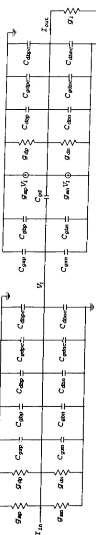
The main building block for the proposed filter structure is a current mir ror, which has a tunable input conductance, gm· Figure 2.1 shows the basic structure. The transistors and Mp
2
constitute the current mirror whereas Mcni,Mcn2
i^cpi «••nd -^cp2 are used to tune the conductances by means o f the two control voltages Kn and V^p. Low-supply voltage characteristics of the circuit comes from the fact that only two transistors exist from supply to ground rail, which enables the circuit operate even at 2 volts.VDD
'-out
Figure 2.1: ^^-tunable current mirror.
Throughout this chapter, we will assume that the tuning transistors McniMcn
2
,Mcpi and Mcp2
are in cut-oif, correspondingly = Vdd and Kn = 0. Therefore our analysis for this chapter will include their only parasitic effects.and we will concentrate on the current mirror. Tuning mechanism and the effect of tuning transistors will be explained in Chapter 3.
To analyze the circuit behaviour, first we assume that p type transistors Afpi and Mp
2
are matched, and n type transistors and M„2 are matched as well. As clear from Fig. 2.1, the two transistors M „i and Mpi are in saturation since Vga = Vd$ for both. In addition, of Mp2
is equal to that of Mpi, and since they are matched, Mp2
is also in saturation. The same argument can be applied to the transistors Af„i and M „2. Having four transistors in saturation, and neglecting output conductances and parasitic capacitances, small signal equivalent circuit can be obtained as in Fig. 2.2.-ou t
S n ^ I ®
Figure 2.2: Small signal model of current mirror.
resulting in where •f«n — 9mV\ (2.1) lout “ 9m Vl (2.2) lout ~ -ftn (2.3) 9m ~ 9mp 'b 9mn (2.4) 9mp = Pp(Vdd-Vb + Vtp) (2.5) 9mn = M V b -V tn ) (2.6)
Including the effect of output conductances and parasitic capacitances, the small signal equivalent circuit becomes as in Fig. 2.3. The circuit can be simplified by combining parallel capacitances and conductances, as shown in Fig. 2.4.
H" ---A\A b) I b) ---sAA/'--- |l' b! “VW— i tn
s
o Obi O Hh t CJ — sA/V^ I — AA^-J -v W '— w v — ''i n
i n
V , - o u t
c ■gd
O n V i ® S b S a
Figure 2.4: Simplified small signal model of current mirror.
KCL at the input and output nodes now yields
ginVi + sCinVi + sC,d{Vi - V
2
) - lin = 0sCgd{V2 —
Vi) + ^mVi +
Q
oV2
-|-
SC
0V
2+
giV
2= 0
substituting lout = giV
2
and rearranging the terms,lout _ — ~gi{gm — sCgd)_____________ where Cgd = Cieq Cin = Coeq ~ Co = goeq — go — gin
[sC ieq ~|· gin\\^Coeq “f" fl'oeç] "I" sCgd{^gm ^Cgd^
Cgdp "H Cgdn Cgd-\- Cin
2Cgtp
+2Cgsn
+2Cgbp
-f2Cgbn
-|-Cdbp - f Cdbpc + Cdbn -I- Cdbnc + Cgdpc + Cgdnc Cgd -f Co Cdbp"h Cdbpcd" Cdbnd" Cdbnc d" Cgdpc d" Cgdnc go + gi gdpd- gdn gm d" gdp d" gdn (2.7) (2.8) (2.9) (2
.10
) (2.11) (2.12) (2.13) (2.14) (2.15) (2.16) (2.17) (2.18)It is clear from Fig. 2.3 that most of the parasitic capacitances appear in parallel at the input stage, between input node and ground. The output conductances of the transistors are added to gm, resulting in an increased input conductance g%n· First parasitic pole is located approximately at gin!Cieq 3.nd the second pole occurs approximately at gocqfCoeq· The capacitance between
Cgdp l .U f F CgdpC 8.399/F Cgdn 2.263 f F CgdnC 0.6034/F Cgsp 6.161/F Cgspc 8.399f F Cgsn 17.55/F CgsnC 0.6034/F Cgbp 8.872/F Cghn 22.18FF Cdbp 6.U5/F Cdbpc 33.95f F Cdbn 10.85/F (^dbnc 3.798/F 9mp 37.57fi(l/n) 9mn 91.6fi{l/n) 9dp 0.8375^(1/0) 9dn 0.7658/i(l/O )
Table 2.1: Parameters obtained from HSPICE
input and output nodes, Cgd·, yields a zero at QmlCgd- Besides directly being added to input and output capacitances, Cgd causes a slight shift in two poles due to the additive term sCgd{gm ~ sCgd) in the denominator of H {s).
The circuit in Fig. 2.1 is simulated using MIETEC 2.0/i technology and the parameters obtained from HSPICE simulations are shown in table 2.1. Using this table, coefficients of the transfer function H {s) given in Eq. 2.9 axe calculated as shown in table 2.2. The output conductance gi is chosen to be equal to gin since it is the admittance seen when an identical block is cascaded.
Cgd 3.703f F C ie, 177.5744/F Coeq 68.0484/F 9m 129.17/x(l/0) 9in 130.7733/i(l/O) 9i 130.7733/i(l/O) 9oeq 132.3766/i(l/0)
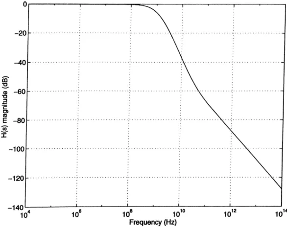
Substituting the calculated paxameters into H (s) given in Eq. 2.9 mag nitude of H (s) is plotted in Fig. 2.5. The first parasitic pole is located at 736A4MHz, whereas the second pole occurs at l.95GHz, Zero of the transfer function is located at 34.9GHz.
Figure 2.5; Magnitude plot of H (s)
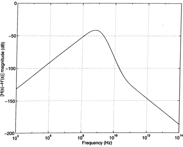
In the denominator of H{s)y the additive term sCgd{gm — sCgd) does not add an extra pole, but slightly shifts the transfer function. In order to show this effect, let us define the following function
9li,9m ^Ggd)
H'(s) =
\sCieq “l· 9in^\.^^oeq "t“ 9oeq\
(2.19)
Magnitude plot of the error function c(s) = [/f(s ) — H'{s)] is plotted in Fig. 2.6. Note that, magnitude of the error caused by the additive term sCgd(9m - sCgd) is below -40dB . Therefore, ignoring this term, we can say that parasitic capacitances and conductances yield 2 poles and a zero, where only the first pole is below gigahertz range.
Figure 2.6: Magnitude plot of e(5) = [/^(5) —
Up to this point, we have analyzed the current mirror with one output stage. Unlike voltage mode circuits, only one circuit block can be connected to the output stage of the current mirror. Therefore, multiple output stages are required for current multiplication and feedback implementation. For the given current mirror structure, this is simply achieved by connecting an inverter together with its tuning transistors to the input node. The configuration is shown in Fig. 2.7. Each output current branch is called a current replica.
In order to use in filter implementation, damped integrator and damped differentiator blocks are constructed using the current mirror and capacitors.
Ji. M.nl VDD ¡4· ' Vp . I . 4 * V , ' ^ -*-out ^ -^out n r II--- II---^cn
Figure 2.7: Current multiplication
2.1
Damped Integrator
'-out
Van
Damped integrator is the basic building block for the construction of low-pass biquadratic filters as well as band-pass biquads. Characteristic function for a damped integrator is given as follows
a H (s) =
s + a
(
2.
20)
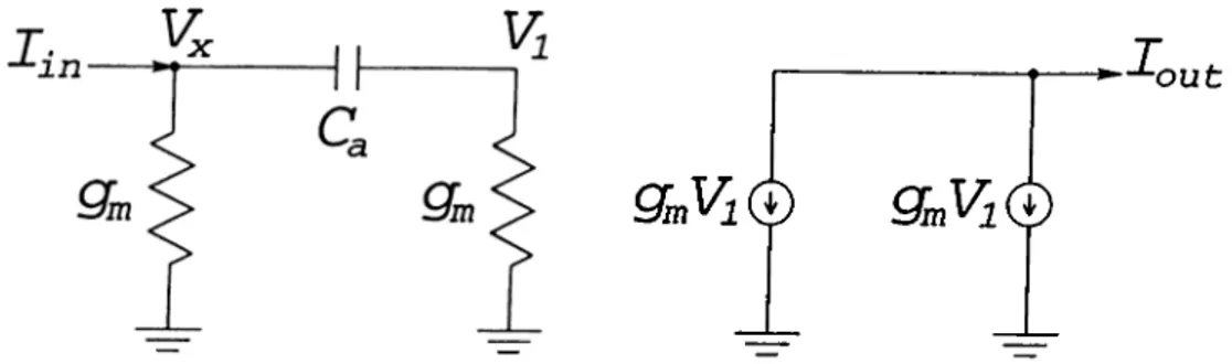
where a is the dominant pole of the circuit. If a capacitor Ca is connected be tween the input node of the current mirror aad ground, small signal equivalent model for the resulting circuit becomes as in Fig. 2.8
-in
Q i
X
o u tFigure 2.8: Small signal model o f damped integrator. KCL at the input and output nodes yields
resulting in lin = {sC a + gm )V l (2.21) I out ~ 5^771^ (2.22) lout 9m (2.23) lin ~ ^ "t" 9m /
11
Further analysis including parasitic capacitances and output conductances yields the same small signal model as in Fig. 2.4, where Cieq is replaced by Cieq + Ca- Since the input conductance is also increased to the dominant pole is shifted to ginl{Ca+(^ieq)· The non-dominant pole is still the same as the second parasitic pole of the current mirror, located at goeqlCoeq- Previously, it is calculated as 1.95GHz, which is located very far from the dominant pole. Consequently, below gigahertz range parasitics do not have a significant effect on the transfer function other than a slight shift of the dominant pole. Cor rection of this shift is possible by tuning, which will be discussed in the next chapter. Therefore, the proposed structure is very suitable for high frequency filter design. VDD I J - ) o u t I (+ ) o u t
Figure 2.9: Differential configuration.
In order to obtain better noise characteristics and wider dynamic range, a fully differential block is needed. This is achieved by connecting two ba sic blocks as shown in Fig. 2.9. Besides providing both positive and negative output currents for feedback implementation, the differential configuration re quires half the capacitance used for the non-differential block for the same
cutoff frequency, which means that area of the capacitors are reduced by a factor of 2.
2.2
Damped Differentiator
Damped differentiator is the basic building block for the design of high-pass biquadratic filters. Also, it can be used in the design of band-pass biquads. Characteristic function of a damped differentiator is given as follows
H (s) =
S CL
(2.24)where a is the dominant pole. For the design of damped differentiator, the input capacitor is placed between the input node of the current mirror and another conductance [gm) block as in Fig. 2.10.
-out
Figure 2.10: Schematic of damped differentiator.
Neglecting the effect of parasitics, the small signal model is obtained as shown in Fig. 2.11.
Writing the node equations
K = /., 1 = /. J_______1_____ 9m “T 1 = /., ^ 5m+*C 9m ~h sC Qmi'isC + gm)
13
(2.25) (2.26) (2.27)X
o u tg m V i ® 9 m V l ®
Figure 2.11: Small signal model o f damped differentiator.
K = V. = /., + 1/-SC 9m + s C
sC
= /. 9 m {‘^ s C 9 m ) (9m + s C )sC
lout — 9 m (^ ^ C d" 9m') —‘^y\9m2sC
2sC
+9,n
resulting in, ^OUt 5 + (2.28) (2.29) (2.30) (2.31) (2.32) (2.33)Detailed analysis shows that parasitic capacitances at the input node are not absorbed in the input capacitance Ca, unlike the low-pass case. Further more, extra gm block at the input stage adds new parasitics to the circuit. Output conductance of the block is also increased as well as output capaci tance, since another current replica is added to get unity high frequency gain. Because o f all these factors, high-pass filter design is restricted to lower fre quencies than in low-pass case. However, the parasitic pole is still beyond some hundreds of megahertz frequency, and filters can be designed within the low VHF range.
Again for noise immunity and feedback implementation, differential block is needed for the damped differentiator. The differential configuration is obtained by just adding another differentiator block with negative input current.
As mentioned in the introduction, in all simulations throughout this thesis
M IETEC 2/j, technology is used. The main limitation is that extracted par asitic capacitance values can be as large as IpF, which is important at high frequencies. If the parasitics are not small compared to input capacitance, the error in the transfer function may be beyond tuning limits. To avoid this, for the same corner frequency, gm can be made larger with larger input capaci tance so that parasitics have less effect. However, large gm means increasing W/L ratios, together with parasitics. Besides, chip area increases. Therefore, increasing gm is not a good solution. Using a better technology, such as 0.7^ brings the frequency range beyond Q.bGHz.
Chapter 3
TUNING
The transfer function of a filter varies considerably due to process variations, temperature effects and aging. The resulting variation in component values and parameters can be as high as 30% of the desired ones. In addition, change of parameters for each transistor is not the same. Therefore, tuning is necessary for continuous time filters in order to correct these errors.
In the proposed structure, tuning is achieved by changing the bias voltage Vb, by either sinking or supplying a constant DC current to the input and output nodes. The input stage of the current mirror is redrawn in Fig. 3.1. The bias voltage Vb can be calculated using the following relation
_ y/KiVdd + Viv) + y/FnVtn
\JWp
+(3.1)
For Pn = and Vtn = -Vfp, Vb is equal to Vjd/2. For > Pp, Vb is less than Vddl‘^·) and vice versa. Typically, treshold voltage of a MOS transistor is 1 volt for n-types, and -1 volt for p-types. Hence Vb voltage is confined between Vdd — 1 = 2F and IF , including the voltage swing caused by the input current.
To explain the tuning mechanism, first let us explain how Qm changes for varying Vb, and then continue with the control mechanism of H.
VDD
М_
£
Vb
Figure 3.1: Input stage of the current mirror.
Writing the Qm relation as given in Eq. 2.4,
9m = M V d i - H + K p ) + ^n{Vb - K n )
rearranging the terms, we have
9m = [^p(ydd + Vtp) — ^nVtn] + Vb(0n — ^p)
(3.2)
(3.3) The first term in Eq. 3.3, which is square-bracketed, is independent of Vb and determined by ratios of the n and p transistors. The second term is the key point for the tuning mechanism. Since variation of the Vb voltage is 1 volts for the best case, maximum variation of Çm is (/0„ — /ip). For a MOS transistor, the transconductance parameter /9 is given as
W
/? = ^f^Co (3.4)
Typically, pn is 2.5-3 times greater than pp, while the oxide thickness Cox is the same for both. Therefore, for equal sized transistors, is readily greater than ^p. Keeping the size of p-type transistors minimum, (/?„ — ^p) factor can be increased by choosing a wider n-type transistor for the current mirror. As a result, the tuning range can be increased by just using wider n transistors. The other way is also possible, that is to keep the size of n transistors minimum and using wider p-type transistor. However, to obtain the same tuning range, p transistors should be much larger, resulting in more chip area. In the analysis, we will use the first approach and have minimum-sized p transistors ensuring that Pn > A>· Looking at Eq. 2.4 more closely, it is obvious that a raise in Vb
causes Qm to increase, which we call up-tuning. Also, down-tuning is achieved by decreasing H together with
gm-Even though increasing W/L ratio of the n transistors also increase the tuning range, it has a negative effect on the input signal swing, which is another bottleneck in low-voltage circuits. Maximum input swing is obtained when the bias voltage Vt is equal to Vdd/2. As discussed earlier, this condition is met when /3n = /^p, resulting in zero tuning range for Vm = -Vtp. Having /?„ > the tuning range increases together with decreasing and decreasing input swing. Therefore, there is a trade-off between input signal swing and the tuning range of the current mirror. Besides, the tuning is not symmetrical when Vb is different from V¿d/2. For our case, down-tuning range is less than up-tuning range. For low-pass filter case, this is more preferrable than the reverse condition, since most of the parasitic capacitances are absorbed in the input capacitor of the filter block, decreasing the corner frequency or shifting it down.
So far, we have discussed the effect of Vb on gm·, but we did not mention how Vb is changed. We will now analyze the up-tuning and down-tuning mechanisms separately. It should be noted that, when down-tuning mechanism is active, up-tuning is off, and vice versa.
3.1
Down-Tuning
As stated earlier, down-tuning is achieved by decreasing the bias voltage H· This is simply carried out by sinking a constant DC current from the input and the output nodes. Since the gate-to-source voltages for the output transistors are the same as those of input ones, bias voltage at the output node is the same as the input bias voltage, H, if the same DC current is sunk from that node. Therefore, our analysis will only include the input stage, and extend it to output stage using matched transistors.
Figure 3.2 shows the down-tuning mechanism at the input stage. The transistor Men is controlled by Kn voltage and it is operated either in cut-off
VD D
14·^--- 1
Figure 3.2: Input stage for down-tuning.
or in saturation region. Assuming that M^ following equation
hn = j { V u ~ V k + V t p f - ^
where Idn is the constant DC current given as
is in saturation, KCL at the input node yields the
(3.5)
(3.6)
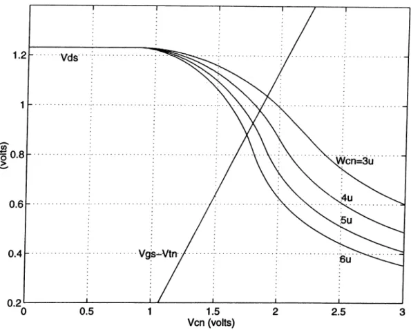
In Eq. 3.6, ^cn is the transconductance parameter of the transistor Men- In order to obtain maximum tuning range, the ratios of the tuning transistor {Wen and Lcn) should be chosen appropriately so that H voltage can be adjusted down to Vtn, and no less than that value since the transistor M „ cease to conduct below that voltage. In Fig. 3.3, V¿s and (V^* — V/n) for varying Ven is plotted for the transistor Men- Length o f the transistor is chosen as 3//, which is the minimum for the technology used.
In the figure, minimum attainable V¡, values, which is equal to Vds, is deter mined by the intersection point of Vds and — Vtn curves. Below that point, the tuning transistor Men operates in the linear region. The point is going down, as the width Wen is increased. However, Vb is already limited by the treshold voltage Vtn, and additional input swing. Therefore, choosing a ratio which allows H to decrease down to 0.6 volts has no meaning other than waste of chip area since it requires wider transistor. In Fig. 3.3, Wen = 4/i seems to be the most appropriate one, and it is chosen for further simulations. If the
Figure 3.3: EiFect of for several
Wen-quiscent Vb voltage for Ven = 0 had been higher, a wider transistor may have been chosen.
Going back to the basic block given in Fig. 2.1, with Mcpi and Mcp
2
are off and the rest in saturation, the small signal model for the circuit is the same as in Fig. 2.4, with the difference in gin and gout as in the following9in — 9m "f· 9dp "I" 9dn "b 9dcn
9o ~ 9dp "b 9dn"b 9dcn
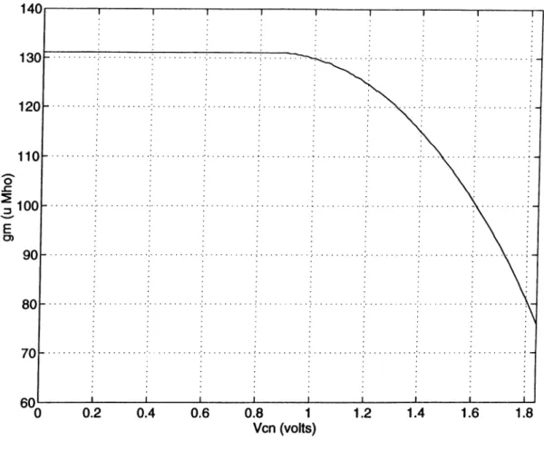
(3.7) (3.8) Resulting in the same transfer function as in Eq. 2.9, the tuning transistors increase the input and the output conductances by a small amount, which is considered as the non-ideal effect of the tuning mechanism. Neglecting this effect, gm decreases considerably, also decreasing the corner frequency. Figure 3.4 shows gm versus plot within the valid range.
Figure 3.4: gm versus V^.
Input conductance of the current mirror is determined by the {W/L) ratios o f the transistors Mn\ and Mp\. In an ideal current mode circuit, input con ductance is equal to infinity, therefore the voltage swing is zero. Due to finite conductance of input stage, a small voltage swing occurs, which also limits the maximum input signal level. Having gin as the input conductance, (H + should be above Vtn and below 3 — Vtp. Since Vh is controlled by means of Vcn·, maximum input swing also depends on Vcn, which is plotted in Fig. 3.5.
As it is clear from the figure, a linear relationship is observed between lout and /,·„ when /,·„ < 50gA. This range can be increased by using wider transistors for the mirror.
Figure 3.5: lout versus
3.2
Up-Tuning
A similar analysis follows for the up-tuning of the current mirror. As in down tuning case, the input stage as shown in Fig. 3.6 is analyzed. In the figure, the transistor Мер is used to supply a DC current to the input node. The current is controlled by Vcp voltage, which also keeps the transistor either in cut-off or in saturation.
Again assuming saturation for the transistor Afep, KCL at the input node yields,
lir = у (H - - ^ ( K u - Ч + (3.9) where I¿p is the current supplied to the node and given as
lip
=
^(V ii
- K, +
Ю '
(3.10)VDD
М. |~lL К р J l · "
Vb
Figure 3.6: Input stage for up-tuning.
This time, the bias voltage Vb is increased, and the amount of increase depends on Vcp and ^cp- The upper limit for VJ, is equal to (Vdd — Цр), including a positive swing caused by input current. In Fig. 3.7, |Vda| and (IV^,! + Vtp) curves for the transistor Мер is depicted for several Wep values, where Lep is chosen as 3/z, which is the minimum length.
Minimum |V^,| values are the intersection points of the curves (|V^s| + Vtp) and |Vds|. Vcp is valid to the right of that point, where the transistor is not in linear region. To locate this intersection point at the optimum value, which is Vdd — Vtp, width of the transistor, Wep, is chosen as 35/i. Further increasing the width causes Vb to rise over 2V within the valid range of Vcp, where Mp gets into cut-oflf region.
The small signal model for the up-tuned circuit, in which Mcni and Mcn
2
are OÍF and others are in saturation, is the same as in Fig. 2.4. The parameters gin and gout also change as in the following9in — 9m “t" 9dp "b 9dn "b 9dcp 9o ~ 9dp T 9dn “f· 9dcp
(3.11) (3.12)
Therefore, the transfer function of the current mirror is still the same as in Eq. 2.9 with minor differences in parameters. As shown in Fig. 3.8, value of gm increases more than twice within the valid range of Vcp, which means that the corner frequency can be tuned up more than twice the original one.
Dynamic range of the current mirror, i.e. maximum allowable input current
Figure 3.7: Effect of Vcp for several
Wcp-amplitude also depends on the control voltage Vcp. In Fig. 3.9, lout versus /,·„ plots for several Vcp voltages are shown. For this case, a linear relationship is observed between /,■„ and lout when /,·„ < 50fiA.
Having the results of both up and down tuning, we will now compare them. Because of the difference in transconductance of the mirror transistors, up and down tuning ranges are not equal. As we discussed earlier, it is better to have wider up-tuning range, considering the effect of parasitics.
Frequency characteristics and up-down tuning curves of the damped in tegrator obtained from HSPICE simulations are depicted in Fig. 3.10. Due to finite output impedances of transistors and other non-ideal effects, a slight decrease in the passband occurs when the filter is tuned.
Figure 3.8: Qm versus Vcp.
Figure 3.9: Vcp versus Ц .
Figure 3.10: Frequency characteristics and tuning curves of the damped inte grator.
Chapter 4
IMPLEMENTATION OF
FILTER BLOCKS
Realization o f filters is carried out by using cascaded biquad synthesis, in which a filter transfer function is decomposed in a cascade o f multiple damped inte grator and damped differentiator blocks. In Chapter 2, basic building blocks were constructed. In this chapter, biquads of low-pass, high-pass and band-pass functions will be synthesized.
In most general form, a biquad can be represented as + kis + ko
U{s) =
+ ^ s + (4.1)
Depending on the coefficients k
2
, k\ and ko, all types of biquads can be obtained [4], [12]. Instead of implementing the function in Eq. 4.1 in general circuit form, we will treat all filter types separately.A low-peiss biquadratic filter is characterized by the transfer function Ko<^o
4.1
Low-pass Biquad Design
H {s) =
+ f s + UJ^ (4.2)
In Eq. 4.2, Kq is the DC gain, Q is the quality factor, and cjq is the resonant frequency o f the filter. For Q values less than 1 / \/2, the magnitude plot has no peak. The case where Q = 1 /v ^ i s referred to as the maximally flat magnitude. For Q > l/\ /2 , the peak occurs at the frequency upq.
Two different approaches for the implementation of the transfer function in Eq. 4.2 are presented in this section. The first approach, the Low-Q biquad, is suitable for filters having low-Q factors. In fact, there is no exact boundary between low and high quality factors. In our analysis, we will treat low quality factor as being less than or equal to 1. The second approach, namely high-Q biquad, can be used in implementation of filters of high-Q factors, as well as low-Q ones.
4.1.1
Low-pass Low-Q Biquad
The first approach for implementation o f a biquad is suitable for low-Q de signs. The filter is composed o f two differential damped integrators which are used in cascade form. Applying a negative feedback from the output to the input, generation of complex poles is achieved. The signal-flow graph of the biquadratic filter is drawn in Fig. 4.1.
a
b
s+a
s+b
lout
Figure 4.1: Signal-flow graph of low-pass low-Q biquad.
Transfer function of the filter structure in Fig. 4.1 is given as follows hut _________ o6(A:/ + 1)_______
lin
+ (a + 6)s + u6(A;/+ 1) where a and b are Qm/C values for each damped integrator.(4.3)
Now, let us find the relationship between Q-factor and the feedback co efficient kf. Without loss of generality, we can choose wq = 1 in order to
simplify the equations. Then the denominator of the low-pass biquad becomes + s/Q + 1. Equating this to the denominator of Eq. 4.3 yields
resulting in for a to be real, A > 0 a b — \ jQ (4.4) ah{kj + 1) = 1 (4.5) a 1 kf + \ ~ (4.6) 1 4 (4.7) Q-^~ kf + l - ^ kf > i Q ^ - l (4.8)
Consequently, it is clear from Eq. 4.8 that for high-Q filters, feedback coef ficient kf, and hence number o f current replicas at the output stage becomes very laxge. This increases non-ideal and parasitic effects considerably as well as the chip area. Furthermore, connecting a large number of output stages in parallel causes the output impedance to decrease, which ideally should be infinity. However, the block can be used in the design of low-Q biquads such as second order Butterworth filter with a Q-factor of 1 /\/2.
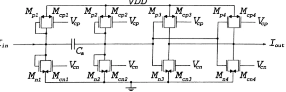
Implementation of the low-Q biquad using MOS transistors is given as in Fig. 4.2. The numbers kf and kf + l represent the number of current replicas, i.e. number of output stages connected in parallel. The two capacitors, Ci and C
2
determine filter coefficients. The frequency characteristics and the tuning curves of a second order low-pass Butterworth filter obtained from HSPICE simulations are shown in Fig. 4.3.Vap. l i n -VDD " S ’ A j ^ A j ' ¿ j t-A-i VDD *-2C ,+ ¿ J kf+ 1 r i - l " r i-* ^ou4'*'^ ^ou4 ^
Figure 4.2: Schematic of low-pass low-Q biquad with MOS transistors.
Figure 4.3: Second order Butterworth filter obtained by using the approach suitable for low-Q applications.
4.1.2
Low-pass High-Q Biquad
The second low-pass biquad structure proposed is aimed to have high-Q with minimum number of transistors. With the existing damped integrator block, which has a transfer function a /(s -f- a), high-Q biquad construction is not practical. Figure 4.4 shows the new first order building block. Originally, it is the same structure as in Fig. 2.1 with a capacitor from the input node to ground, except for a feedback current of —2Iout which is fed to the input node.
V D D
-lout
Figure 4.4: Basic building block for low-pass high-Q biquad.
The simplified small signal model is the same as in Fig. 2.2, with the input current as /,„ — 2/out- KCL at the input and output nodes yields
resulting in ~ 2 /o u t = {sCa+gm)Vi (4.9) lo u t ^ 9m^l (4.10) lou t 9mf(^a (4.11) ^ 9m! Ca
Hence the first order block with a transfer function a / {s-a ) can be realized. Implementation of the fully differential block is shown in Fig. 4.5.
The block itself has an unstable behaviour due to the pole on the right hand side of s-plane. In order to obtain a stable biquad, this block is combined with the previous one, as in Fig. 4.6. The transfer function of this structure is given as I nh
(4.12)
^out ab lin + { a - f>)s -I- ab32
VDD
I (+)out
out
—^
-2
Figure 4.6: Signal-flow graph of low-pass high-Q biquad.
Using Eq. 4.12, high-Q filters can be easily implemented. The biquad is stable as long as (a — 6) > 0. For high-Q filters, (a — h) becomes very small and with the effect of parasitics it can be negative. This error is eliminated by tuning each first order blocks separately. Since the dc gain of the block is 1, no extra current replicas axe needed at the output stage.
Implementation of the biquad using MOS transistors is given in Fig. 4.7. Using this schematics and only changing capacitances, a wide range of filters can be implemented. Frequency characteristics and the tuning curves of a second order Butterworth filter obtained from HSPICE simulations is depicted in Fig. 4.8.
Vc,'cp
VDD
A -i rA-i rcjiJ |-A-| pcU
Y 2 _ ^ Vcn. Q t v d d ^2--¿ - I r i- i ^ Y i - · . . Y i ^ [C? |-C3-I (-ClJ |-C ^ Ft 5=^ ^ou4^) 4 3 •I'ou/->»
Figure 4.7: Schematic of low-pass high-Q biquad with MOS transistors.
Figure 4.8: Second order Butterworth filter obtained using high-Q biquad structure.
Characteristic equation for a high-pass biquad is given as follows Kos^
4.2
High-pass Biquad Design
H {s) = (4.13)
As in the low-pass case, two approaches for the design of high-pass biquads are presented. The first one is the Low-Q biquad, suitable for low-Q applica tions and the second one is high-Q biquad.
4.2.1
High-pass Low-Q Biquad
High-pass low-Q biquad includes two damped differentiator blocks in cascade form. The signal flow graph for the biquad structure is shown in Fig. 4.9. As in the low-pass case, the numbers kj and kj + 1 represent the number of current replicas.
Figure 4.9: Signal-flow graph of high-pass low-Q biquad. Transfer function of the biquad in Fig. 4.9 is
lout
2 I .a±L o 4-
^ ^ kf+l^ ^ kf+l
(4.14)
where a and b corresponds to values for each first damped differentiator. Quality factor of the biquaxl again depends on the feedback factor kj. For simplicty, let u>o = 1, then
ab fc/ + 1 (1 b
kf + 1
= 11
(4.15)
1
Q(4.16)
35
rearranging the terms,
9
.
a H —— a + [kj + 1) = 0 for a to be a real number, A > 0,
(% + 1)^ Q 2 -4 (A :/ + 1) > 0 kj > 4 g ^ - l (4.17) (4.18) (4.19)
Clearly, for high Q values, kj increases drastically, making biquad design impractical due to the reasons discussed in the low-pass case.
4.2.2
High-pass High-Q Biquad
In order to obtain high-Q biquad, again a first order high-pass block which has a transfer function s/{s — a) is needed. Similar to low-pass case, a positive current of —2Iout is fed to the input node of the damped differentiator given in Fig. 2.10. With an input current of (/,·„ — 2Iout), resulting small signal model is the same as in Fig. 2.11. Using Eq. 2.33 transfer function for the new block is found as (4.20) (4.21) rearranging. 2/ouO = = ^out s lin * Q __ 3m. 2C (4.22)
Note that the minus sign does not appear in the transfer function. Since s /( s — a) type first order block is obtained, flow graph for the high-Q biquad can be drawn as in Fig. 4.10.
Transfer function o f the filter in Fig. 4.10 is found as ^OUt
-f (6 — a)s -|- ab
(4.23)
out
Figure 4.10: Signal-flow graph of high-pass high-Q biquad.
4.3
Band-pass Biquad
Band-pass second order function is given as
Hb p(s) = 52 + ^ 5+ ^ . (4.24) The first approach in band-pa^s biquad design is suitable for moderate-Q filters, which have a quality factor up to 3. Biquads are realized by using either two damped integrators, or a damped integrator and a damped differentiator block. Signal flow graphs for the two methods are shown in Figs. 4.11 and 4.12.
1
Figure 4.11: Signal-flow graph o f band-pass biquad using two damped integra tors.
s+b
out
kf
Figure 4.12: Signal-flow graph of band-pass biquad using a damped integrator and a damped differentiator.
Transfer functions corresponding to the two signal flow graphs are the same and given as
H U ) =
as
+ (6 — {kf — l)a )s + ab In order to have unity pass-band gain,
a — b — (kf — l)a
(4.25)
(4.26) Simplifying, we obtain b = kja. Quality factor of the biquad is then calculated as follows Q = a
u>o
= \ / ^ =ctyfkf
Q = (4.27) (4.28) (4.29)Therefore, in both methods the quality factor is equal to which means that only moderate-Q filters can be implemented. Since kf is the number of feedback current replicas, construction of high-Q filters (such as 10) is not practical. Besides, for unity DC gain, b is equal to kfa, which is difiBcult to implement for high kf values due to pareisitic effects. The second structure is more preferrable since it requires approximately half the number of transistors used in the first one for the same kf.
The second approach allows high-Q band-pass biquad design, by using a damped integrator and a first order section with a transfer function b/(s — b). The corresponding signal flow graph is shown in Fig. 4.13.
1
Figure 4.13: Signal-flow graph of band-pass biquad for high Q-factor
The transfer function of the biquad in Fig. 4.13 is
lout as
5^ + (a — b)s + ab (4.30)
Choosing u^o = 1 for simplicity, the quality factor Q and the pass-band gain A are calculated as follows
a — b = a b = 1 1 Q a — b — 1 A = aQ = 0^ — 1 (4.31) (4.32) (4.33) (4.34) Rearranging the terms the following relationship is obtained between A and Q.
A = ^ ^ ‘ (4.35)
Clearly, for high Q values, the passband gain A is approximately equal to Q, whereas A approaches unity as Q goes to zero.
The transfer function given in Eq. 4.30 can also be obtained by combining a damped differentiator and a first order high-pass section of s/(s — 6) in a similar manner.
Chapter 5
EXPERIMENTAL RESULTS
Measurement of the filter characteristics in high-frequency range requires spe cial precautions. The proposed filter topology is current-mode whereas all measurement devices operate in voltage-mode. Therefore, a test circuit should be designed in order to obtain the transfer function of the circuit accurately. Figure 5.1 shows the experimental setup.
'm o ]
A M P
— ^
V
-'out
Figure 5.1: Test circuit.
Since each filter block has differential input current, a transformer is con nected to the input stage in order to convert single-ended input to differential one. At the output stage, another transformer converts the differential out put current to single-ended. Input impedance of the network analyzer, which measures Vout voltage, is equal to 50il. Without an amplifier at the output of the filter, the pass-band voltage gain {Vout/Vin) is measured as —46dR, as the input impedance of the filter is approximately 10A;fi. For this case, it is impossible to measure the filter characteristics correctly because of the noise
level of network analyzer and capacitive coupling through the circuit board, which severely deteriorates the transfer function. Therefore, an RF amplifier is necessary to compensate the loss caused by 50i) output load. Magnitude and phase response of the amplifier is given in Figs. 5.2 and 5.3, respectively.
Figure 5.2: Magnitude response of the amplifier.
Using the test setup in Fig. 5.1, two Butterworth filters were tested. The amplifier has approximately 24.5dJ3 gain, which is not sufficient to compen sate the loss caused by impedance mismatch. Nevertheless, it enables us to obtain the filter characteristics. The band-pass gain is normalized to QdB for magnitude plots. Figure 5.4 and 5.5 shows the magnitude and phase response of seventh order low-pass Butterworth filter with iM H z cutoff frequency, re spectively. The magnitude plot shows that the measured cutoff frequency is approximately 5.3MHz. The shift in corner frequency can also be observed in the phase plot.
Figure 5.3: Phase response of the amplifier.
The second filter block tested is seventh order low-pass Butterworth filter with 10.7MHz cutoff frequency. Magnitude and phase plots axe given in Figs. 5.6 and 5.7. Cutoff frequency is measured as approximately \2MHz. The shift in filter response is due to fabrication tolerances, as well as parasitic effects caused by experimental setup.
Figure 5.4: Magnitude response o f seventh order low-pass Butterworth filter with AM H z cutoff frequency.
Figure 5.5: Phase response of seventh order low-pass Butterworth filter with AM H z cutoff frequency.
Figure 5.6: Magnitude response of seventh order low-pass Butterworth filter with 10.7MHz cutoff frequency.
Figure 5.7: Phase response of seventh order low-pass Butterworth filter with lO.TMHz cutoff frequency.
Chapter 6
CONCLUSION
A new current-mode differential filter structure is proposed. The filter struc ture is suitable for low supply voltages and high frequency applications. In order to correct fabrication tolerances and parasitic effects, a tuning mecha nism is introduced. By using two control voltages, filters can be tuned down to 50%, and up to 130% o f their corner frequencies. Automatic tuning can be implemented using one o f the schemes in the literature [6], [13]-[17].
Implementation of low-pass, high-pass and band-pass filters are demon strated in the thesis. Among them, the most suitable for high frequency ap plications is low-pass filters, in which parasitics are absorbed in the input ca pacitance and do not deteriorate the transfer function below gigahertz range. For high-pass filters, the effects of parasitics are more severe, causing parasitic poles within several hundreds of megahertz range. Nevertheless, biquads hav ing high-Q factors can be obtained for both high-pass and low-pass functions. For band-pass filters, moderate-Q biquads are implemented using two methods. In addition, high-Q biquads can be realized using another approach. However, pass-band gain is not equal to unity, and it becomes nearly the same as Q for high-Q values.
As long as HSPICE simulation results are concerned, the proposed topology allows the design of filters beyond 0.5GHz frequency. The available frequency
range depends on the technology used. However, at high frequencies, HSPICE analysis may not be valid.
Higher order filters are synthesized by cascading multiples of biquadratic and first order sections. Two test chips including several filter blocks have been designed. The first one includes a current mirror, a first order low-pass block, three Butterworth biquads and two Chebyshev biquads. The first chip has been submitted for fabrication to the MIETEC Alcatel 0.7/i M PW run on December 1994. The second chip contains three of seventh order Butterworth filters and four band-pass biquads with different resonant frequencies and Q- factors. This chip has been submitted to the MIETEC Alcatel 2.0/x M PW run on March 1995.
REFERENCES
[1] J. S. Martinez, M. Steyaert, and W. Sansen, High Performance CMOS Continuous Time Filters, Kluwer Academic Publishers, Boston, 1993.
[2] Y. P. Tsividis and J. 0 . Voorman, Integrated Continuous-Time Filters, IEEE Press, New York, 1993.
[3] Y. P. Tsividis, “Integrated Continuous-Time Filter Design - An Overview,” IEEE J. Solid-State Circuits, vol. 29, no. 3, pp. 166-176, March 1994.
[4] R. Unbehauen and A. Cichocki, MOS Switched-Capacitor and Continuous-Time Integrated Circuits and Systems, Springer-Verlag, Berlin, 1989.
[5] B. Nauta, “A CMOS Transconductance-C Filter Technique for Very High Frequencies,” IEEE J. Solid-State Circuits, vol. 27, no. 2, pp. 142-153, Feb. 1992.
[6] B. Nauta, Analog CMOS Filters for Very High Frequencies, Kluwer Aca demic Publishers, Boston, 1993.
[7] R. H. Zele, D. J. Allstot, and T. S. Fiez, “Fully Balanced CMOS Current- Mode Circuits,” IEEE J. Solid-State Circuits, vol. 28, no. 5, pp. 569-574, May 1993.
[8] S. S. Lee, R. H. Zele, D. J. Allstot, and G. Liang, “CMOS Continuous- Time Current-Mode Filters for High-Frequency Applications,” IEEE J. Solid-State Circuits, vol. 28, no. 3, pp. 323-328, March 1993.
[9] J. Ramirez-Angulo, M. Robinson, and E. Sanchez-Sinencio, “Current- Mode Continuous-Time Filters: Two Design Approaches,” IEEE Trans. Circuits and Syst. II: Analog and Digital Signal Processing, vol. 39, no. 6, pp. 337-341, June 1992.
[10] S. S. Lee, R. H. Zele, and D. J. Allstot, “A Continuous-Time Current- Mode Integrator,” IEEE Trans. Circuits and Syst., vol. 38, no. 10, pp. 1236-1238, Oct. 1991.
[11] R. H. Zele, S. S. Lee, and D. J. Allstot, “A 3V-125 MHz CMOS Continuous-Time Filter,” Proc. of the Int. Symp. on Circuits and Sys tems (ISCAS ’93), Chicago, IL, pp. 1164-1167, 1993.
[12] D. E. Johnson, Introduction to Filter Theory, Prentice-Hall, New Jersey, 1976.
[13] F. Krummenacher and N. Joehl, “A 4-MHz CMOS Continuous-Time Filter with On-Chip Automatic Tuning,” IEEE J. Solid-State Circuits, vol. 23, no. 3, pp. 750-758, June 1988.
[14] R. Schaumann and M. A. Tan, “The Problem of On-Chip Automatic Tuning in Continuous-Time Integrated Filters,” IEEE Proc. ISCAS, pp. 106-109, 1989.
[15] K. A. Kozma, D. A. Johns, A. S. Sedra, “Automatic Tuning of Continuous-Time Integrated Filters Using an Adaptive Filter Technique,” IEEE Trans. Circuits and Syst., vol. 38, no. 11, pp. 1241-1248, Nov. 1991.
[16] J. Silva-Martinez, M. Steyaert, and W. Sansen, “A Novel Approach fot the Automatic Tuning of Continuous Time Filters,” IEEE Proc. ISCAS, pp. 1452-1455, 1991.
[17] J. M. Khoury, “Design of a 15-MHz CMOS Continuous-Time Filter with On-Chip Tuning,” IEEE J. Solid-State Circuits, vol. 26, no. 12, pp. 1988- 1997, Dec. 1991.
APPEN D IX A
LAYOUTS
Figure A.l: Layout of the low-pass low-Q biquad (MIETEC 0.7/i).
Figure A.2: Layout of the first test chip (MIETEC 0.7//).
Figure A.3: Layout of 7th order Butterworth low-pass filter (MIETEC 2.0^).