1
A GATE MODULATED DIGITALLY
CONTROLLED MODIFIED CLASS-E AMPLIFIER
FOR ON-COIL APPLICATION IN MRI
A THESIS SUBMITTED TO
THE GRADUATE SCHOOL OF ENGINEERING AND SCIENCE
OF BILKENT UNIVERSITY
IN PARTIAL FULFILLMENT OF THE REQUIREMENTS FOR
THE DEGREE OF
MASTER OF SCIENCE
IN
ELECTRICAL AND ELECTRONICS ENGINEERING
BY
BISMILLAH NASIR ASHFAQ
MARCH, 2018
ii
A Gate Modulated Digitally Controlled Modified Class-E
Amplifier for On-Coil Application in MRI
By Bismillah Nasir Ashfaq March, 2018
We certify that we have read this thesis and that in our opinion it is fully adequate, in scope and in quality, as a thesis for the degree of Master of Science.
Ergin Atalar (Advisor)
Abdullah Atalar
Ali Bozbey
Approved for the Graduate School of Engineering and Science:
Ezhan Karaşan
iii
ABSTRACT
A Gate Modulated Digitally Controlled Modified Class-E Amplifier for
On-Coil Application in MRI
Bismillah Nasir Ashfaq
M.S. in Electrical and Electronics Engineering Advisor: Ergin Atalar
March, 2018
The switch-mode RF power amplifiers, known for their high output power capability and good efficiency, have proved valuable for on-coil applications in MRI hardware. The class-D and class-E amplifier topologies have been demonstrated to be promising candidates to replace the conventional inefficient linear RF power amplifiers used in MR hardware which are placed away from the scanner room. Conventionally, the amplitude modulation of the output waveform in such switch-mode RF power amplifier applications is achieved either by implementing an amplitude modulation block at the drain of the amplifier, or by encoding the amplitude modulation information in the phase of the carrier signal at the gate of the amplifier. Both these approaches require additional hardware, thus increasing the cost and complexity of the system.
Considering the aforementioned background, a novel technique of modulating both the amplitude and frequency of the output waveform, without the need for any additional hardware other than the driver circuitry for the amplifier itself, is presented and implemented for class-E amplifier topology. At 64 MHz (1.5 T), the analytical models of the amplifier for both the switch-on and switch-off cases are first derived and implemented in software. The period of the digital carrier signal at the gate of the amplifier is then divided into k bits, where k is greater than 2. It is then noted that both the amplitude and frequency of the output waveform can be controlled by altering this digital input in a certain manner. For a typical 2 ms 1.5 T MRI RF pulse, the digital carrier bitstream would consist of k × 128000 bits. This would require testing 2k×128000 bitstream combinations to achieve the desired output waveform, requiring infeasible computational power. It is however shown that by
iv
intelligently programming the bitstream patterns for a selected number of periods, and by repeating those patterns for a chosen duration of time, the desired amplitude and frequency modulation of the output waveform can be achieved. The normalized root mean square error (NRMSE) for a 2 ms sinc pulse designed using such an approach is calculated to be 11%. The designed bitstreams are tested on hardware as well, both in bench-top and MRI experiments. Bench-top experiment results correlate well with the software predictions. The amplifier shows a peak drain efficiency of 89% at 50 W input power. The MR images obtained at 50 W input power using a 2 ms sinc pulse designed using the presented approach show no artifacts.
The ultimate goal of the current research is to design a 32-channel transmit array coil for the MRI, capable of delivering a total of approximately 10 kW output power. Each amplifier element should therefore be able to deliver about 300 W output power. In this regard, further research needs to be conducted to achieve such output power level using the presented modulation approach. Nonetheless, the approach is general and can be implemented to other switch-mode RF power amplifier topologies as well. It promises to provide a performance equivalent to the other modulation approaches while reducing the overall cost and complexity of the system at the same time.
Keywords: RF Power Amplifiers, Class-E Amplifier, Modulation Techniques, Gate Modulation,
v
ÖZET
MRG’de Bobin Üzeri Uygulama için Kapı Kiplemeli Sayısal Kontrollü
Değiştirilmiş Sınıf-E Güç Yükselteci
Bismillah Nasir Ashfaq
Elektrik ve Elektronik Mühendisliği, Yüksek Lisans Tez danışmanı: Ergin Atalar
Mart, 2018
Yüksek çıkış gücü kapasitesi ve iyi verimliliği ile tanınan anahtarlamalı RF güç yükselteçleri, MRG donanımındaki bobin uygulamaları için değerli olduğunu kanıtladı. Sınıf-D ve sınıf-E güç yükselteci topolojilerinin, MR donanımında kullanılan ve tarayıcı odasının dışına yerleştirilen geleneksel verimsiz doğrusal RF güç yükselteçlerinin yerine ümit verici adaylar olduğu kanıtlanmıştır. Geleneksel olarak, bu tür anahtar özellikli RF güç amplifikatör uygulamalarında çıkış dalga formunun genlik kiplemesi, ya güç yükseltecinin kanalında bir genlik kipleme bloğu uygulanarak ya da genlik kipleme bilgisinin, taşıyıcı sinyalin fazındaki genlik kipleme bilgisinin yükseltecinin kapısında kodlanmasıyla elde edilir. Her iki yaklaşım da ek donanım gerektirir, böylece sistemin maliyetini ve karmaşıklığını arttırır.
Yukarıda bahsedilen önbilgi göz önüne alındığında, güç yükseltecinin kendisi için sürücü devresinden başka herhangi bir ek donanıma ihtiyaç duymadan çıkış dalga formunun hem genliğini hem de frekansını kiplemeye yönelik yeni bir teknik, E sınıfı amplifikatör topolojisi için sunulmakta ve uygulanmaktadır. 64 MHz'de (1.5 T), hem açma-kapama durumları için güç yükseltecinin analitik modelleri ilk olarak yazılımda türetilir ve uygulanır. Güç yükseltecinin kapısındaki dijital taşıyıcı sinyalin periyodu daha sonra k'nin 2'den büyük olduğu k bitlerine bölünür. Daha sonra çıkış dalga formunun genliğinin ve frekansının bu dijital girişin uygun bir şekilde değiştirerek kontrol edilebileceğine dikkat çekilir. Tipik bir 2 ms 1.5 T MRG RF darbesi için, dijital taşıyıcı bit akışı k × 128000 bitten oluşacaktır. Bu, istenen çıktı dalga formunu elde etmek için 2(k × 128000) bit akışlı birleşimlerinin test edilmesini gerektirebilir ve bu da olası
vi
akıllıca programlanmasıyla ve bu desenlerin seçilen bir süre boyunca tekrarlanmasıyla, çıkış dalga formunun arzu edilen genlik ve frekans kiplemesinin gerçekleştirilebileceği gösterilmiştir. Böyle bir yaklaşım kullanılarak tasarlanmış bir 2 ms sinc darbesi için normalleştirilmiş kök ortalama kare hatası (NRMSE) %11 olarak hesaplanmıştır. Tasarlanan bit akışları, hem tezgâh üstü hem de MRG deneylerinde donanımda da test edilir. Tezgâh üstü deney sonuçları, yazılım tahminleriyle iyi bir ilgileşim göstermektedir. Amplifikatör 50 W giriş gücünde %89'luk bir tepe kaynak verimi gösterir. Sunulan yaklaşımı kullanarak tasarlanmış bir 2 ms sinc darbesi kullanılarak 50 W giriş gücünde elde edilen MR görüntüleri hiçbir artifakt olmadığını göstermektedir.
Mevcut araştırmanın nihai amacı, toplam yaklaşık 10 kW çıkış gücü sunabilen, MRG için 32 kanallı bir iletim dizisi bobini tasarlamaktır. Her amplifikatör elemanı bu nedenle yaklaşık 300 W çıkış gücü sunabilmelidir. Bu bağlamda, sunulan modülasyon yaklaşımını kullanarak böyle bir çıktı gücü seviyesine ulaşmak için daha fazla araştırma yapılması gerekmektedir. Bununla birlikte, yaklaşım geneldir ve diğer anahtarlamalı RF güç amplifikatörü topolojilerine de uygulanabilir. Sistemin genel maliyetini ve karmaşıklığını aynı anda azaltırken diğer kipleme yaklaşımlarına eşdeğer bir performans sağlamayı vaat ediyor.
Anahtar Kelimeler: RF Güç Yükselteçleri, Sınıf-E Güç Yükselteci, Kipleme Teknikleri, Kapı
vii
ACKNOWLEDGEMENT
I would like to express my earnest gratitude to my graduate advisor Prof. Dr. Ergin Atalar for his constant guidance, patience, and motivation throughout the project. Also I appreciate Prof. Dr. Abdullah Atalar and Assoc. Prof. Dr. Ali Bozbey for being my jury members.
I acknowledge my earnest gratitude to Berk Silemek, Fatima Tu Zahra, Uğur Yilmaz, Redi Poni, and Mertcan Han for their contributions in this work. Berk was responsible for implementing the FPGA codes for this work. I thank you Berk for being an amazing team member and for your time and dedication, and also for translating the abstract into Turkish. Thank you Fatima for making me understand the important details about the previously developed hardware and for your time and contribution in MRI experiments. Uğur Yilmaz was responsible for writing the MRI pulse sequences which enabled the acquisition of MR images and k-space data. Thank you Uğur for your time and help. I am thankful to Redi Poni for his guidance in developing the analytical models of the amplifier. Mertcan Han, a summer intern, developed the MATLAB GUI (discussed in Section 3.4.1) for speeding up the design process. I thank you Mertcan for your contributions.
Additionally, I am thankful to all the members of the UMRAM research group for providing a warm and pleasant research environment. Thank you Uğur and Aydan Hanım for baking all the yummy cakes.
Last but not the least, I am immensely grateful to my dear mother, the iron lady, without whose indestructible strength of character and limitless struggle after the early death of our father, and without whose constant prayers and unconditional love for her children, none of this could have ever been possible, and I am thankful to my dear wife Fatima Tu Zahra for her ultimate and constant support throughout this journey.
viii
CONTENTS
A GATE MODULATED DIGITALLY CONTROLLED MODIFIED CLASS-E AMPLIFIER FOR
ON-COIL APPLICATION IN MRI ... 1
ABSTRACT ... iii ÖZET... v ACKNOWLEDGEMENT ... vii CONTENTS ... viii LIST OF FIGURES ... xi LIST OF TABLES ... xv CHAPTER 1 ... 1 INTRODUCTION ... 1 CHAPTER 2 ... 4 THEORY ... 4
2.1. Conventional Class-E Amplifier Design ... 4
2.1.1. The Chosen RF Power Transistor Device for Hardware ... 7
2.2. Earlier Proposed Design Modifications ... 9
2.3. Driving the Amplifier – A Brief Overview ... 10
2.4. The Conventional Supply Modulation Approach and Introducing the Concept of Gate Modulation ... 11
2.5. Analytical Modeling of the Amplifier Waveforms ... 13
2.5.1. Model 1: Constant-Current Source Assumption at Drain ... 13
2.5.2. Model 2: Inductor Assumption at Drain ... 23
CHAPTER 3 ... 33
METHODS ... 33
3.1. Amplifier Model Implementation ... 33
3.1.1. Implementation ... 34
ix
3.2. The Gate Modulation Algorithm ... 37
3.2.1. Running the Amplifier’s Circuit Simulator Model at Different Duty Cycles ... 38
3.2.2. Running the Amplifier’s Analytical Models at Different Duty Cycles ... 39
3.2.3. Achieving Amplitude Modulation Using Only k = 4 Bits per Cycle ... 40
3.2.4. The Effect of Shifting the bits and Achieving Phase-Modulation ... 41
3.2.5. Meaning of 0101 and when it should be used… ... 43
3.3. The Desired Amplitude and Frequency Modulated Waveform ... 44
3.4. Algorithm Implementation in Software ... 45
3.4.1. The MATLAB GUI (Graphic User Interface) ... 46
3.4.2. Designing a Sinc Pulse of Duration 200 μs with a Subsection Duration of 6.25 us ... 46
3.4.3. Designing a Sinc Pulse of Duration 200 μs with a Subsection Duration of 3.125 us ... 47
3.4.4. Quantization Levels vs. Subsections – Generalizing the Approach and Designing a Sinc Pulse of Duration 2 ms ... 47
3.5. Hardware Implementation ... 48
3.5.1. Driver Implementation ... 49
3.5.2. Class-E Amplifier Implementation ... 50
3.5.3. Amplifier PCBs Used for the Experiments ... 51
3.6. Experimental Setup for Bench-top Experiments ... 53
3.6.1. Carrier Bitstream Re-optimization on Hardware ... 54
3.7. Experimental Setup for MRI Experiments ... 55
3.7.1. FPGA Implementation Errors and Synchronization Issues – Identifying the potential problems and methods used to resolve them ... 57
CHAPTER 4 ... 61
RESULTS ... 61
4.1. Amplifier Models’ Implementation – Simulation Results ... 61
4.1.1. Model 1 – Constant-Current Source Assumption at Drain ... 61
4.1.2. Model 2 – Inductor Assumption at Drain ... 62
4.1.3. Circuit Simulator Model Results – Comparison and Verification of the Implementation of Analytical Models ... 64
4.2. Circuit Simulator Results at Multiple Duty Cycles ... 65
4.3. Gate Modulation Algorithm – Simulation Results ... 67
x
4.3.2. Sinc Pulse of Duration 200 μs (Subsection Duration: 3.125 μs) ... 69
4.3.3. Sinc Pulse of Duration 2 ms ... 72
4.4. Hardware Implementation Results ... 73
4.5. Gate Modulation Algorithm – Experimental Results ... 74
4.5.1. Bench-top Experiments Results ... 74
4.5.2. MRI Experiments Results ... 77
CHAPTER 5 ... 79
DISCUSSION AND CONCLUSION ... 79
xi
LIST OF FIGURES
Fig. 2.1 – Conventional class-E amplifier ... 5 Fig. 2.2 – Modified class-E amplifier design. The RF choke inductor had been replaced with an equivalent transmission line. The transmit coil was designed such that it served as the load network of the amplifier as well. The driver and FPGA blocks are also shown. [2] ... 9 Fig. 2.3 – Three-stage wideband driver design [2, 3] ... 10 Fig. 2.4 – The gate modulation concept illustrated. By removing the supply modulation block, and by controlling the digital input of the gate of the amplifier, it is aimed to achieve both the amplitude and frequency modulation of the output waveform. ... 12 Fig. 2.5 – Amplifier model 1 schematic. An ideal constant-current source is assumed instead of the RF choke inductor at the drain of the amplifier. The transistor is replaced by an ideal switch with zero internal losses. ... 14 Fig. 2.6 – The schematic diagram for the switch-on case of the amplifier model 1 ... 14 Fig. 2.7 – Amplifier model 2 schematic. The previous ideal constant-current source assumption in model 1 is now replaced by an RF choke inductor assumption at the drain of the amplifier. Again, an ideal, lossless switch is considered in place of the transistor. ... 23 Fig. 2.8 – The schematic diagram for the switch-on case of the amplifier model 2 ... 24 Fig. 2.9 – The schematic diagram for the switch-off case of the amplifier model 2 ... 26
Fig. 3.1 – The effects of adjusting the load network components on the switch-voltage waveform [35] ... 34 Fig. 3.2 – Schematic diagram of the class-e amplifier model with realistic switch ... 35 Fig. 3.3 – The load-network tuning environment in the circuit simulator ... 37 Fig. 3.4 – The desired sinc waveforms each of duration 200 μs. a) The desired sinc waveform with one main lobe and two side lobes. b) The desired sinc waveform with one main lobe. ... 44 Fig. 3.5 – Block diagram of the hardware implemented to test the designed bit-streams ... 48
xii
Fig. 3.6 – The block diagram showing different components of the 3-stage driver circuit [2, 3] ... 50 Fig. 3.7 – Modified design layout of the amplifier PCB to include the equivalent micro-strip transmission line integrated on board (dimensions: 65 mm by 50 mm) ... 52 Fig. 3.8 – The design layout of the amplifier PCB including the supply modulation block as well as the integrated micro-strip transmission line (dimensions: 100 mm by 50 mm) [2]... 52 Fig. 3.9 – The block diagram of the experimental setup for bench-top experiments [3]. ... 53 Fig. 3.10 – The hardware setup for bench-top experiments. The FPGA sends the LVDS signals to the amplifier PCB (consisting of the driver and amplifier circuitry). An external transmission line equivalent to RF choke inductor is shown connected at the drain of the amplifier. The output waveform is monitored on the oscilloscope via a 2 cm diameter receiver coil placed near the transmit coil loaded with phantom. ... 54 Fig. 3.11 – The block diagram of the experimental setup for MRI experiments ... 55 Fig 3.12 – MRI experiment setup: Inside the scanner room – The amplifier PCB was connected to the custom made square-loop transmit coil placed on top of the 8-channel receiver head coil, and the cylindrical phantom placed under the head coil was excited with the custom generated 2 ms sinc pulse while the scanner’s transmit system was off. ... 56 Fig 3.13 – The k-space magnitude of the data from a single receive channel obtained from the MRI experiment conducted with phase encoding turned off. It can be observed from the diagram that the discontinuity occurs in the transmission of the RF pulse a total of six times in this specific case. ... 57 Fig 3.14 – The ‘Acquisition Setup’ settings implemented for the ‘Segmented Sampling Mode’ of the oscilloscope, used to record the consecutive gate and output waveforms of the amplifier... 58 Fig. 3.15 - The k-space magnitude of the data from a single receive channel obtained from the MRI experiment conducted with phase encoding turned off after the implementation errors in the FPGA code were resolved. It can be observed from the diagram that no discontinuities occur in the transmission of the RF pulse. ... 59 Fig. 3.16 – The updated setup in the systems room. A 10 MHz signal is generated by the FPGA and is fed to the signal generator and the scanner spectrometer for synchronization ... 60
Fig. 4.1 – The amplifier model 1 implementation results. a) Switch voltage and switch current vs. time. b) Switch current vs. time. c) Output voltage and output current vs. time. ... 62
xiii
Fig. 4.2 – The amplifier model 2 implementation results. a) Switch voltage vs. time. b) Output voltage and output current vs. time. c) Drain current vs. time (Zoomed-out). d) Zoomed-in version of the drain current vs. time at steady-state. ... 63 Fig. 4.3 – The circuit simulator implementation results. a) Gate voltage vs. time. b) The drain current vs. time. c) The switch-voltage vs. time. d) The output voltage and output current vs. time. ... 65 Fig 4.4 – Peak output voltage vs. the duty cycle of the gate input signal for the ADS model of the class-E amplifier ... 66 Fig. 4.5 – a) Input and output power vs. the duty cycle of the gate input signal for the ADS model of the class-E amplifier. b) Associated drain efficiency vs. the duty cycle. ... 67 Fig. 4.6 – Power dissipated in the switch vs. the duty cycle of the gate input signal for the ADS model of the class-E amplifier ... 67 Fig. 4.7 – The desired (left) and predicted (right) output waveforms for the sinc pulse of duration 200 μs with a subsection duration of 6.25 μs. ... 68 Fig. 4.8 – (a) The predicted output waveform plotted on top of the desired output waveform for the sinc pulse of duration 200 μs with a subsection duration of 6.25 μs. (b) Zoomed-in version of the same plot for one of the subsections. ... 69 Fig. 4.9 – The overlapped FFT plots of the desired and predicted output waveforms. (a) The FFT plots in 1 MHz bandwidth show no harmonic peaks. (b) The FFT plots in 0.2 MHz bandwidth are shown. The FFT plots of the desired and designed output waveforms show 9.7 dB and 11.2 dB amplitude respectively at the center frequency (64 MHz). ... 69 Fig. 4.10 – The desired (left) and predicted (right) output waveforms for the sinc pulse of duration 200 μs with a subsection duration of 3.125 μs. The spikes observed in the amplitudes of the predicted output waveform (right) correspond to the transient states of each subsection and are minimized based on careful designing of the bit-stream patterns. ... 70 Fig. 4.11 – (a) The predicted output waveform plotted on top of the desired output waveform for the sinc pulse of duration 200 μs with a subsection duration of 3.125 μs. (b-c) Zoomed-in versions of the same plot for two of the subsections. ... 71 Fig. 4.12 – The overlapped FFT plots of the desired and predicted output waveforms. (a) The FFT plots in 1 MHz bandwidth show no harmonic peaks. (b) The FFT plots in 0.1 MHz bandwidth are shown. The FFT plots of the desired and designed output waveforms show 26.6 dB and 19 dB amplitude respectively at the center frequency (64 MHz). ... 71
xiv
Fig. 4.13 – The desired (left) and predicted (right) output waveforms for the apodized sinc pulse of duration 2 ms ... 72 Fig. 4.14 – The overlapped FFT plots of the desired and predicted output waveforms. (a) The FFT plots in 1 MHz bandwidth show no harmonic peaks. (b) The zoomed-in version is shown. The FFT plots of the desired and designed output waveforms show 26.4 dB and 19 dB amplitude respectively at the center frequency (64 MHz). ... 73 Fig. 4.15 – Hardware implementation results when the amplifier PCB is run with a 50% duty cycle signal at the gate of the amplifier (0011). a) LVDS signals sent by the FPGA to the driver part of the amplifier PCB. b) The signal at the output of the driver part and input to the gate of the amplifier. c) Switch-voltage vs. time. ZVS and ZVDS conditions are satisfied. ... 74 Fig. 4.16 – Gate modulated output waveform of the amplifier when the carrier bit-stream designed for a duration of 200 μs with a subsection duration of 6.25 μs is implemented... 75 Fig. 4.17 – Gate modulated output waveform of the amplifier (200 μs, subsection duration 6.25 μs) and the associated FFT in 1 MHz bandwidth. ... 76 Fig. 4.18 – Gate modulated output waveform (red) of the amplifier when the carrier bit-stream designed for a duration of 2 ms is implemented. The overlapped drain current profile (yellow) is also shown (right side). ... 77 Fig. 4.19 – Gate modulated output waveform of the amplifier (2 ms) and the associated FFT in 2 MHz bandwidth. The FFT shows a 14.135 dBm peak value at the central frequency (64 MHz) with a 10 dB difference in magnitude to the nearest harmonic components under a bandwidth of 2 MHz. ... 77 Fig. 4.20 – MR image obtained at 50 W input power (TE/TR = 15ms/200ms). The ghosting artifacts observed in the phase encoding direction (left to right) are associated with the phase inconsistencies and synchronization issues. ... 78 Fig. 4.21 – MR image obtained at 50 W input power (TE/TR = 15ms/200ms) at different FOV (Field of Views) after the phase inconsistencies and synchronization issues have been resolved... 78
xv
LIST OF TABLES
Table 3.1 – Characteristic parameters of BLF573 ... 36 Table 3.2 – Examples of different bit-stream patterns for m = 2, 4, 6 ... 41 Table 3.3 – The effect of applying circular shift to the designed bit-stream pattern on the amplitude and phase of the output waveform ... 42
1
CHAPTER 1
INTRODUCTION
In conventional applications of the switch-mode radio-frequency (RF) power amplifiers, the amplitude/envelope modulation is achieved by applying the modulating signal at the drain of the amplifier [1] while the frequency modulation is achieved by a carrier signal applied at the gate of the amplifier. The implementation of such an amplitude modulation block requires additional hardware at the drain of the amplifier and the approach is often referred to as the supply modulation approach. One method of implementing such an amplitude modulation block is detailed in [2, 3] where the duty cycles of the digital input signals applied to the amplitude modulation block were controlled in order to obtain various envelope shapes of the modulating signals at its output. The resulting modulating signals were then low-pass filtered and applied at the drain of the amplifier to achieve the envelope modulation of the desired output signal.
In other applications namely delta-sigma based transmitter applications [4, 5], the time varying baseband modulating signal is encoded to a bi-level constant envelope signal using a technique called the delta-sigma modulation (DSM) [6]. The resulting signal is then frequency modulated using a frequency up-converter and fed to the input of the gate of the power amplifier (PA). The aim is to contain all the information only in the phase of the signal while maintaining a constant envelope for the signal. A few of the drawbacks of this approach include the need for a high clock speed to oversample the data to achieve good signal quality,
2
and the problem of the quantization noise which forms most part of the signal at the output of the DSM, affecting the signal quality. For more details on these issues and how they are dealt with, the reader is referred to [4].
An emerging application that the switch-mode RF power amplifiers are recently finding is in the hardware of Magnetic Resonance Imaging (MRI). MRI is a non-invasive imaging technique that utilizes a constant magnetic field B0, a radiofrequency magnetic field B1, and multiple
gradient magnetic fields (G) to produce high quality images of different parts of the body [7] including brain, chest, abdomen, etc. One of the important building blocks of the MRI system is the RF transmit chain which consists of a frequency synthesizer, a modulator, an amplifier and a transmit coil. The frequency synthesizer generates a continuous sinusoidal carrier wave at the Larmor frequency [7]. The modulator then modulates this carrier wave with a desired envelope signal to obtain the desired pulse shape in the order of milliseconds. The amplifier amplifies the resulting modulated pulse to the required level to achieve certain flip angle. And finally, the transmit coil transmits the modulated pulse to excite the body part under examination.
The commercially available MRI scanners employ linear, low efficiency power amplifiers which are placed in the systems room (situated behind the scanner room) and require cooling systems due to their high power loss. The amplifiers are situated away from the transmit coils which are either located within the inner walls of the scanner or as free-standing devices near or on the patient. This distance between the amplifiers and the transmit coils requires that long transmission cables be used, increasing in turn the overall complexity and cost of the system while further decreasing its overall efficiency.
For the excitation purposes, the birdcage coil [8] has widely been used as the standard transmit coil in MRI due to its high efficiency and homogeneity. Its performance, however, has been reported to be degraded and resulting in lower SNR (signal-to-noise ratio) in case of higher filed strengths (greater than 3 T). Multi-channel transmit array systems (also referred to as parallel transmit systems) are therefore proposed as an alternative to such conventional systems. The several advantages of the parallel transmit systems [9] include
3
more degree of freedom in terms of controlling each transmit element separately, local area excitation, and multiple slice selectivity. B1 field uniformity and homogeneity are reported to
be improved [10-12], and the system has also shown to be advantageous in terms of improving RF shimming and increasing the imaging speed [13-15]. Additionally, parallel transmit systems have shown to be advantageous in terms of SAR (Specific Absorption Rate) reduction as the applied RF power and the region of excitation can both be controlled more precisely [16, 17]. RF heating on long metallic implants is also shown to be reduced by being able to control and steer the electric field in parallel transmit systems [18, 19]. Despite its enormous advantages, there are however some challenges that arise when it comes to the implementation of a parallel transmit system. Increasing the number of coil elements in the system inherently increases its complexity as the required amount of cabling for separate power lines and control signals for each element increases. Another concerning issue is the unnecessary coupling among the adjacent elements which not only causes a decline in the efficiency but also artifacts in the images resulting from the undesired B1+ fields in the
neighboring coils.
In an attempt to simplify the RF chain design to be more compatible with the parallel transmit systems, the different components of the RF chain including the pulse modulator, the amplifier, and the transmit coil are worked on to be integrated into a single unit. This is the point where the applications of switch-mode RF power amplifiers come into play in MRI. Several novel designs of on-coil RF power amplifiers have been proposed in this regard with the aim that all three functions, i.e., the pulse modulation, signal amplification, and the RF excitation, are performed at one place. The pulse modulation techniques that are usually employed in such designs include the more conventional supply modulation approach or the recently emerging delta-sigma based transmitter approach. Gudino proposed a current-mode class-D amplifier configuration in her work and tested her design at 1.5 T as well as higher field strengths [20-22]. The research group at UMRAM chose to work on class-E amplifier configuration as it is even more suited for on-coil amplifier applications due to its desirable topology and ability to achieve theoretically 100% efficiency [23].
4
The class-E amplifier topology was initially proposed by Sokal and Sokal [23], with further work on developing the design equations performed by Raab [24, 25] and other authors [26, 27] over the years. The conventional class-E amplifier configuration consists of a switch, an RF choke inductor, and a load network consisting of a shunt capacitance, a series resonance circuit (or a parallel resonance circuit (shunt filter) as presented in [28]), and the load. This topology is considered ideal for MRI applications as the transmit coil itself can be modeled as the load network of the amplifier. By tuning the coil to the Larmor frequency and matching it to the optimum load impedance of the amplifier, the need for any additional 50 ohm matching is removed. Additionally, as an on-coil configuration, the need for long transmission cables carrying the RF power from the amplifier to the transmit coil is also eliminated.
For the past few years, extensive research has been carried out at UMRAM for developing and implementing a feasible model of the class-E amplifier that is both compatible with the MRI and capable of achieving the desired output power at high efficiency [2, 3, 29-32]. In these works, the RF choke inductor was replaced by an equivalent transmission line for MR compatibility and the transmit coil was implemented as the load network of the amplifier. An output power of 100 W from a single amplifier was first reported at an efficiency of 88%. Later, 300 W output power was achieved from a single amplifier at 84% efficiency. The amplifier’s performance under several constraints including its performance in 1 MHz bandwidth and at high temperature, and the effects of load variation on the efficiency of the amplifier were also studied. The effects of increasing the number of coil elements to two and the resulting coupling performance of the system were also analyzed. In all these works, however, the primary approach used for modulating the envelope of the pulse shape over the carrier frequency was the supply modulation approach.
An alternative approach to modulating the envelope of the desired pulse shape, named as the digital modulation approach, was first presented in [2]. The idea was to remove the supply modulation block altogether and to achieve both the amplitude and frequency modulation of the output signal only be controlling the digital input bit-stream at the gate of the transistor. The expected benefits of such an approach would include reduced cost and
5
complexity of the circuit while striving to achieve an equivalent performance. In this work, the idea of digital modulation for switch-mode RF power amplifiers is revisited and redeveloped from a new perspective, drawing on the concepts of pulse width modulation for non-linear systems and delta-sigma based transmitters. The technique is named as the gate modulation approach based on its implementation method, and though could be implemented to other non-linear switch-mode RF PA configurations as well, the class-E topology is chosen to work on based on its promising applications as an on-coil amplifier configuration in the MRI.
Chapter 2 of this work starts with a brief account of the conventional class-E amplifier topology and the earlier modifications done for making it compatible with the MRI. The concept of gate modulation is then introduced followed by a detailed account of the analytical modelling of the amplifier to develop its complete software model. In chapter 3, the methods used for the implementation of the amplifier model in software are presented, and the gate modulation algorithm is explained in detail. The methods used for software and hardware implementation of the technique are then presented while highlighting the important challenges along the way. In chapter 4, the associated results of the amplifier’s software model implementation and of the gate modulation algorithm implementation both in software and hardware (including bench-top and MRI experiments) are presented, while the discussion on those results and the final conclusion points are presented in chapter 5.
4
CHAPTER 2
THEORY
This chapter starts with a brief overview of the conventional class-E amplifier design and its working principles. The earlier proposed design modifications to make the amplifier compatible for use in MRI are then highlighted, including replacing the RF choke inductance with a transmission line as well as integrating the transmit coil as a part of the load network of the amplifier. The implemented driver circuitry is then briefly explained along with the conventional modulation approach implemented previously. After explaining this essential background information, the concept of gate modulation, a novel method developed to modulate both the amplitude and frequency of the desired radiofrequency pulse (RF-pulse) without the need for supply modulation, is introduced. Implementation of this method involves several steps, from analytical modelling of the amplifier to running simulations and hardware tests. In this chapter, the analytical modelling of the amplifier is presented while the implementation of these models and further details on gate modulation algorithm are left to be discussed in later chapters.
2.1. Conventional Class-E Amplifier Design
The class-E power amplifier is a highly efficient, tuned, switched-mode power amplifier consisting of a load network and a single transistor that operates at the carrier frequency of the output signal. The load network consists of a shunt capacitance Cshunt connected in
5
parallel to the transistor (this includes the internal drain-to-source capacitance Cds of the
transistor as well as an externally connected shunt capacitance C1), and a series-tuned output
circuit which may have a residual reactance as well. The amplifier diagram is shown in Fig. 2.1 which shows the DC supply voltage VDD, the RF-choke inductor L1 which ensures a constant
DC current from the supply voltage, the transistor Q which in ideal case acts as a switch, the external shunt capacitance C1, the series-tuned LC resonance circuit consisting of an inductor
L2 and a capacitor C2, and finally the load impedance R.
Fig. 2.1 – Conventional class-E amplifier
The ideal optimum operation of the class-E amplifier requires that both the voltage across the switch and its time-derivative be equal to zero at the time of switching (the conditions which are formally known as ZVS (Zero-Voltage Switching) and ZVDS (Zero-Voltage Derivative Switching) conditions), ensuring that there is no power loss in the switch. Provided that the on-resistance of the transistor (Rds_on) is zero (ideal switch condition) and the load network is
perfectly tuned and lossless as well, the class-E amplifier can theoretically achieve 100% efficiency in its optimum operation. On the other hand, if the voltage across the switch or its time-derivate are not equal to zero at the time of switching, it will lead to suboptimum operation of the amplifier [24]. In this work, at the stage of deriving the amplifier’s model and implementing it in software, the circuit parameters are going to be derived considering 50% duty cycle and optimum operation conditions of the amplifier. But later, when the gate modulation algorithm will be introduced and implemented, the amplifier’s operation would
6
become suboptimum as the amplifier would then be working at multiple duty cycles. Since the circuit parameters were initially derived based on 50% duty cycle operation and would not be updated as the duty cycle changes, it would ultimately result in affecting the efficiency of the amplifier. This can be considered as a conscious trade-off that was kept in mind while proceeding with the algorithm.
Following assumptions have been made while deriving the design equations for the initial implementation of the amplifier circuit parameters:
1) The switch is considered ideal, meaning that Rds_on is equal to zero.
2) The switch operates at 50% duty cycle.
3) The value of the RF choke inductor L1 is high enough to block the RF signal.
4) The value of the quality factor is assumed high enough to ensure a strictly sinusoidal output current.
5) All the components in the circuit are considered ideal (lossless).
Based on these assumptions, the loaded quality factor (QL) based design equations as found
in the literature [27, 33-35], that will be used in this work to obtain the initial values for R, C1,
C2 and L2, are presented below:
𝑅 = ((𝑉𝐷𝐷) 2 𝑃𝑜𝑢𝑡 ) 0.58 (1 − 0.45 𝑄𝐿 − 0.4 𝑄𝐿2) (2.1) 𝐶1 = 1 34.2𝑓𝑅(1 + 0.9 𝑄𝐿 − 1 𝑄𝐿2 ) + 0.6 (2𝜋𝑓)2𝐿 1 (2.2) 𝐶2 = 1 2𝜋𝑓𝑅( 1 𝑄𝐿− 0.1) (1 + 1 𝑄𝐿− 1.8) − 0.2 (2𝜋𝑓)2𝐿 1 (2.3) 𝐿2 =𝑄𝐿𝑅 2𝜋𝑓 (2.4)
7
Where Pout is the output power desired to be delivered to the load, QL is the loaded quality
factor of the load network, VDD is the supply voltage at the drain of the amplifier, and f is the
frequency of operation of the amplifier (1.5 T scanner).
In the case that the switch is nideal, the power loss in the switch due to the nzero on-resistance of the switch, as analyzed by Sokal and Raab in [25], can be written as follows:
𝑃𝑅𝑑𝑠_𝑜𝑛 = 1.37𝑅𝑑𝑠_𝑜𝑛
𝑅𝐿 𝑃𝑜𝑢𝑡 (2.5)
In this case, the maximum drain efficiency can be calculated as follows:
𝜂 = 𝑅𝐿
𝑅𝐿 + 1.37𝑅𝑑𝑠_𝑜𝑛 (2.6)
2.1.1. The Chosen RF Power Transistor Device for Hardware
Considering again the ideal (lossless) switch case, and the 50% duty cycle operation of the amplifier, the relationship between the output power Pout, the DC supply voltage VDD, and the
load impedance R, as described in [24], can be written as follows:
𝑃𝑜𝑢𝑡 =(𝑉𝐷𝐷) 2
1.74𝑅 (2.7)
Also, the relationship between the peak value of the switch voltage VC1_peak and the DC supply
voltage VDD, again at 50% duty cycle operation of the amplifier, can be written as follows:
𝑉𝐶1_𝑝𝑒𝑎𝑘 = 3.56𝑉𝐷𝐷 (2.8)
Now, as is evident from (2.7) and (2.8), both Pout and VC1_peak are directly proportional to VDD.
This means that in order to achieve a higher value of the output power at 50% duty cycle operation of the amplifier, VDD should be increased, but increasing VDD would cause the peak
value of the switch voltage to increase as well as is evident from (2.8). Based on the specifications of the MOSFET, there’s an upper limit to the peak value of the switch voltage, exceeding which would cause damage to the device; this should be kept in mind while
8
selecting the device. Additionally, as can be seen from (2.6), the drain efficiency of the amplifier is inversely proportional to the on-resistance of the MOSFET (Rds_on). It can also be
observed from (2.6) that the value of Rds_on must be lower than the load impedance RL in
order to avoid any degradation in the efficiency. A MOSFET with higher limiting value of VC1_peak and a lower value of Rds_on is therefore desired.
Before this work, other members of the research group at UMRAM had already been working on the conventional supply modulation based class-E amplifier prototypes for the prospective applications in MRI [2, 3]. The ultimate aim of the research group has been to construct a 32-channel transmit array with on-coil amplifiers, capable of transmitting a total of approximately 10 kW power to the body coil, thus requiring each amplifier prototype to provide an output power of 300 W. Based on the points explained in the earlier passages and the requirements of the MRI just mentioned, a 300 W LDMOS RF power transistor (Ampleon, BLF573, Nijmegen, The Netherlands) had already been selected and was being tested in simulations and on hardware. Four-layered PCB prototypes had been designed and fabricated in the lab and were being tested for on-coil applications in MRI. After the gate modulation algorithm was developed in software, it was therefore possible to use the same PCBs for the associated hardware experiments in this work.
It must be noted here that the selected transistor model BLF573 has an Rds_on = 0.09 ohm,
and VC1_peak = 110 V. Based on the load-pull analysis performed in [3] and on the value of the
load impedance measured on hardware, the value of RL = 1.5 ohm. From (2.6), the calculated
efficiency therefore comes out to be approximately 92.4%. Considering the DC supply voltage VDD equal to 30 V, the value of VC1_peak comes out to be 106.8 V which is well under the limiting
value of 110 V. It shall be kept in mind, however, that these calculations have been performed keeping in mind 50% duty cycle operation of the amplifier. Once the gate modulation algorithm is introduced and implemented, the efficiency and VC1_peak will be affected.
9
2.2. Earlier Proposed Design Modifications
The points explained in this section have been worked on in quite detail in previous works [2, 3]. The reader is therefore referred to the mentioned references to develop a detailed understanding on the subject. Here, a brief overview on the subject is provided. In order to make the amplifier compatible with the MRI, the conventional class-E amplifier design had been modified as shown in Fig. 2.2.
Fig. 2.2 – Modified class-E amplifier design. The RF choke inductor had been replaced with an equivalent transmission line. The transmit coil was designed such that it served as the load
network of the amplifier as well. The driver and FPGA blocks are also shown. [2]
The RF choke inductor L1 had been replaced with an equivalent short coaxial transmission
line, which in later designs was also integrated on the amplifier PCB. The detailed analysis on replacing the RF choke inductor with an equivalent transmission line can be found in [2, 3]. Also, the transmit coil used for the excitation purposes had been designed such that it served as the load network of the amplifier as well. The inductance of the coil served as the equivalent of L2 from Fig. 2.1, i.e., the inductance of the resonance circuit of the amplifier.
The three distributed capacitors C21, C22, and C23, used for tuning of the coil, also collectively
served as the equivalent of C2 from Fig. 2.1, i.e., the capacitance of the resonance circuit of
the amplifier. The load inductance R was provided by the loading of the coil by either phantom or the body.
10
The advantages of designing such an on-coil amplifier configuration have also been mentioned in [2, 3]. First, in such design, the coil serves as both the tuning element of the load network of the amplifier and the RF excitation element for the load in the MRI. Second, as detailed in [3], by using the load pull analysis, the input impedance of the coil is designed so as to match with the optimum load impedance of the amplifier, thus achieving the highest efficiency point. And finally, being an on-coil amplifier structure significantly reduces the transmission line losses which otherwise, in conventional configurations where the amplifiers are placed in the systems room away from the coil, would be significant.
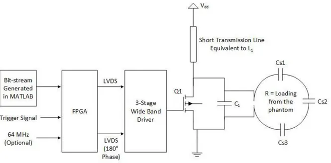
The amplifier is fully digitally controlled by the FPGA, which transmits the designed carrier bit-streams to the gate of the transistor via a driver circuitry. The details on the design of and modifications in the driver circuitry can be found in [2, 3]. Here, a brief overview of the driver circuit is presented as follows.
2.3. Driving the Amplifier – A Brief Overview
To drive the LDMOS transistor BLF573, a 3-stage wideband digitally controlled driver had been designed and implemented. The designed bit-streams were transmitted from KCU105 FPGA evaluation board (Xilinx Inc., California, USA) to the driver circuitry as low voltage differential signals (LVDS). LVDS signaling shows better noise performance as compared to single ended signals. Fig. 2.3 shows the block diagram of the designed driver.
11
The FPGA takes as its input a trigger signal and a frequency signal from the signal generator. The value of the frequency signal is set based on the implementation of the FPGA code and may vary from implementation to implementation. The FPGA then transmits the programmed carrier bit-stream (the details on which will be provided later) to the driver circuit in the form of LVDS signals. Two LVDS signals are transmitted with a 180⁰ phase shift in order to control the high and low sides of the driver. At first stage of the driver circuit, these LVDS signals are converted to single ended signals. At second stage, these single ended signals are sent to the non-inverting current-feedback op-amp configuration whose gain is set to approximately 1.5. In the third and final stage, the output signals from the second stage drive the push-pull MOSFETs which in turn drive the main transistor of the class-E amplifier configuration by charging and discharging its gate capacitance. Delay control between the high-side and low-side of the push-pull driver circuit was achieved using the FPGA.
2.4. The Conventional Supply Modulation Approach and
Introducing the Concept of Gate Modulation
In order to excite the load in MRI, the output pulse of the amplifier must have a specific shape. In small angle approximation, the flip angle is proportional to the magnitude of the FT (Fourier transform) of RF pulse shape. Therefore apodized sinc pulses are commonly used but other RF pulse designs also exist. In conventional applications of the class-E amplifier, while the frequency modulation is achieved through the gate of the transistor, the amplitude/envelope modulation is achieved via an additional supply modulation block implemented at the drain of the transistor. The details on the implementation of such a supply modulation block can be found in [2, 3]. In this work, the gate modulation approach is suggested as an alternative approach to achieve both the amplitude and frequency modulation of the desired output pulse.
Conceptually speaking, the aim is to remove the supply modulation block at the drain of the amplifier, and to achieve both the amplitude and frequency modulation of the output waveform by only controlling the digital gate input signal of the transistor. In typical 50% duty cycle operation of the amplifier, the digital gate signal of the transistor can be considered as
12
a uniform sequence of ones and zeros, where each one or zero represents the half duration of the entire period at the frequency of operation. Thus a bit-stream sent by the FPGA in case of such nominal 50% duty cycle operation would be 101010···. The idea of manipulating the carrier bit-stream to a pattern other than 101010··· in order to achieve the amplitude and frequency modulation was first introduced in [2], but at that stage, each cycle was still considered to be consisting of only two bits, not allowing enough flexibility for design.
In this work, the idea of manipulating the carrier bit-stream was revisited and reconstructed, and as will be explained in detail in the next chapter, it was observed that by dividing each cycle of the carrier waveform into more than two bits per cycle, and by manipulating those bits in a certain manner and transmitting them to the gate of the transistor, it was possible to achieve various amplitude levels of the output waveform in addition to achieving the frequency modulation (concept illustrated in Fig. 2.4). In order to realize such a concept, however, both the switch-on and switch-off modes of the class-E amplifier operation needed to be analytically modelled and implemented in software like MATLAB (The MathWorks, Inc., Natick, Massachusetts), so that different carrier bitstream patterns could be designed and tested by running them on such amplifier models.
Fig. 2.4 – The gate modulation concept illustrated. By removing the supply modulation block, and by controlling the digital input of the gate of the amplifier, it is aimed to achieve both the
amplitude and frequency modulation of the output waveform.
The following section presents, therefore, a detailed account of the mathematical analysis and derivations of the amplifier waveform equations necessary to implement the amplifier models in software. Two different amplifier models are considered at this stage.
13
2.5. Analytical Modeling of the Amplifier Waveforms
Before digging into the gate-modulation algorithm in detail in the next chapter, the task at hand is to derive and implement a working model of the class-E amplifier in software, and verify that model by performing and comparing simulations using standard circuit simulator software (e.g. Advanced Design System (ADS)).
Two different models of the class-E amplifier were considered for this purpose. In the first model (model 1), a constant-current source assumption was made at the drain of the amplifier for reducing complexity. For reasons explained in later chapters, this amplifier model necessitated to be updated to include the RF choke inductor at drain (model 2), replacing the constant-current source assumption made in case of model 1.
For both models, the switch was considered ideal (zero loss), and the amplifier operation was broken down to two modes: switch-on and switch-off. State-space matrix representations were written for both these modes, from which the essential waveform equations were derived. The mathematical workflow for both models is detailed in the following subsections, while their implementation will be explained in the next chapter.
2.5.1. Model 1: Constant-Current Source Assumption at Drain
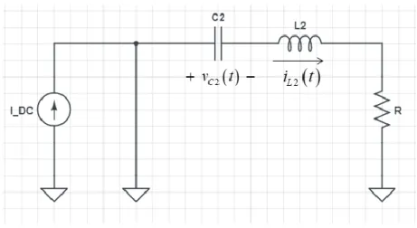
Fig. 2.5 shows the schematic of this model. A constant-current source 𝐼𝐷𝐶 is assumed at the
drain of the amplifier. The switch is considered ideal. The unknown state-variables of interest are 𝑖𝐿2(𝑡), 𝑣𝐶2(𝑡) and 𝑣𝐶1(𝑡). Let’s start our analysis with the switch-on case as follows.
14
Fig. 2.5 – Amplifier model 1 schematic. An ideal constant-current source is assumed instead of the RF choke inductor at the drain of the amplifier. The transistor is replaced by an ideal switch with
zero internal losses.
2.5.1.1 Switch-On Case:
Fig. 2.6 shows the schematic for the switch-on case for the amplifier model 1.
Fig. 2.6 – The schematic diagram for the switch-on case of the amplifier model 1
It can be observed from Fig. 2.6 that the circuit for switch-on case is source-free, which means that we will be investigating the natural response of the circuit in this case. Let’s start our analysis by writing the state-space matrix representation for this case. By Kirchhoff’s Voltage Law (KVL), we can write:
15 ⇒ 𝑣𝐶2(𝑡) + 𝐿2𝑑𝑖𝐿2(𝑡) 𝑑𝑡 + 𝑅𝑖𝐿2(𝑡) = 0 (2.10) ⇒ 𝑑𝑖𝐿2(𝑡) 𝑑𝑡 = − 𝑅 𝐿2𝑖𝐿2(𝑡) − 1 𝐿2𝑣𝐶2(𝑡) (2.11) where 𝑖𝐿2(𝑡) = 𝑖𝐶2(𝑡) = 𝐶2𝑑𝑣𝐶2(𝑡) 𝑑𝑡 (2.12) ⇒ 𝑑𝑣𝐶2(𝑡) 𝑑𝑡 = 1 𝐶2𝑖𝐿2(𝑡) (2.13)
Here, we note that during the time when the switch is on, voltage across the switch, or equivalently, across the shunt capacitor 𝐶1 is equal to zero (ideal switch assumption).
𝑣𝐶1(𝑡) = 0 (2.14)
Combining (2.11), (2.13), and (2.14), we can write the state-space matrix representation as follows: 𝑑 𝑑𝑡[ 𝑖𝐿2(𝑡) 𝑣𝐶2(𝑡) 𝑣𝐶1(𝑡) ] = [ − 𝑅 𝐿2 − 1 𝐿2 0 1 𝐶2 0 0 0 0 0] [ 𝑖𝐿2(𝑡) 𝑣𝐶2(𝑡) 𝑣𝐶1(𝑡) ] (2.15)
Now, let’s derive the explicit expressions for state-variables 𝑖𝐿2(𝑡) and 𝑣𝐶2(𝑡). From the
state-space matrix representation above, we can write:
𝑑𝑖𝐿2(𝑡) 𝑑𝑡 + 𝑅 𝐿2𝑖𝐿2(𝑡) + 1 𝐿2𝑣𝐶2(𝑡) = 0 (2.16)
16
Taking derivative on both sides of the above equation, we get:
𝑑2𝑖 𝐿2(𝑡) 𝑑𝑡2 + 𝑅 𝐿2 𝑑𝑖𝐿2(𝑡) 𝑑𝑡 + 1 𝐿2 𝑑𝑣𝐶2(𝑡) 𝑑𝑡 = 0 (2.17)
Combining (2.13) and (2.17), we get:
𝑑2𝑖𝐿2(𝑡) 𝑑𝑡2 + 𝑅 𝐿2 𝑑𝑖𝐿2(𝑡) 𝑑𝑡 + 1 𝐿2𝐶2𝑖𝐿2(𝑡) = 0 (2.18) Equation (2.18) is a second-order differential equation of the type:
𝑑2𝑦(𝑡)
𝑑𝑡2 + 2𝜁𝜔0
𝑑𝑦(𝑡) 𝑑𝑡 + 𝜔0
2𝑦(𝑡) = 0 (2.19)
where 𝑦(𝑡) is the unknown variable, 𝜔0 is the undamped natural frequency with dimensions
of radians/second, and 𝜁 is the damping ratio, a dimensionless parameter [36]. Comparing (2.18) with (2.19), 𝜔0 and 𝜁 in our case can be defined as follows:
𝜔0 = 1 √𝐿2𝐶2 (2.20) 𝜁 = 1 2𝑅√ 𝐶2 𝐿2 ⁄ (2.21)
The associated characteristic equation can be written as follows:
𝑠2+ 2𝜁𝜔0𝑠 + 𝜔02 = 0 (2.22)
The roots of the characteristic equation (2.22), also known as the natural frequencies, the
characteristic frequencies, or the critical frequencies of the circuit, can be written as follows:
𝑠1,2 = (−𝜁 ± √𝜁2− 1) 𝜔
17
Inserting in (2.21) the optimum values of R, C2 and L2 that we obtained in Section 2.1, we find
that 0 < 𝜁 < 1, meaning that the circuit for switch-on case has an underdamped natural
response, in which case √𝜁2− 1 = 𝑗√1 − 𝜁2 (𝑗 = √−1) and the roots of the characteristic
equation become: 𝑠1,2 = 𝛼 ± 𝑗𝜔𝑑 (2.24) where 𝛼 = −𝜁𝜔0 (2.25) and 𝜔𝑑 = 𝜔0√1 − 𝜁2 (2.26)
Here, 𝛼 is called the damping coefficient, and 𝜔𝑑 is called the damped natural frequency.
Inserting the values of 𝜔0 and 𝜁 from (2.20) and (2.21) into (2.25) and (2.26), we get:
𝛼 = − 𝑅 2𝐿2 (2.27) 𝜔𝑑 = √4𝐿𝐶2 2 − 𝑅 2 2𝐿2 (2.28)
And finally the solution to the equation (2.18) for the case of underdamped natural response can be written as follows:
𝑖𝐿2(𝑡) = 𝐴exp(𝛼𝑡) sin(𝜔𝑑𝑡 + 𝜃) (2.29)
where A and 𝜃 are the initial condition constants, and can be derived as follows:
At time t = 0, we have from equation (2.29):
𝑖𝐿2(0) = 𝐴 sin 𝜃 ⇒ 𝐴 =𝑖𝐿2(0)
sin 𝜃 (2.30)
18 𝑑𝑖𝐿2(0)
𝑑𝑡 = 𝐴(𝛼 sin 𝜃 + 𝜔𝑑cos 𝜃) (2.31)
Inserting t = 0 in (2.11), and combining it with (2.31), we get:
𝐴(𝛼 sin 𝜃 + 𝜔𝑑cos 𝜃) = − 𝑅
𝐿2𝑖𝐿2(0) − 1
𝐿2𝑣𝐶2(0) (2.32) Inserting the value of A from (2.30) and solving for 𝜃, we get:
𝜃 = cot−1{
−𝑅𝑖𝐿2(0) − 𝑣𝐶2(0)
𝐿2 − 𝛼𝑖𝐿2(0)
𝜔𝑑𝑖𝐿2(0) } (2.33)
The expression for 𝑣𝐶2(𝑡) can either be derived from the state-space matrix representation
of (2.15) or we can write from (2.10) as follows:
𝑣𝐶2(𝑡) = −𝑅𝑖𝐿2(𝑡) − 𝐿2𝑑𝑖𝐿2(𝑡)
𝑑𝑡 (2.34)
Inserting in the above equation the expression for 𝑖𝐿2(𝑡) from (2.29), and solving for 𝑣𝐶2(𝑡)
results in the following expression:
𝑣𝐶2(𝑡) = −(𝑅 + 𝛼𝐿2)𝑖𝐿2(𝑡) − 𝜔𝑑𝐴𝐿2exp(𝛼𝑡) cos(𝜔𝑑𝑡 + 𝜃) (2.35)
19
2.5.1.2 Switch-Off Case:
The schematic for the switch-off case of the amplifier model 1 is the same as shown in Fig. 2.5 earlier. It can be observed from Fig. 2.5 that the circuit for switch-off case has a DC forcing element 𝐼𝐷𝐶, which means that we will be investigating the transient response of the circuit
in this case. Let’s start by deriving the state-space matrix representation. By Kirchhoff’s Voltage Law (KVL), we can write:
𝑣𝐶1(𝑡) = 𝑣𝐶2(𝑡) + 𝑣𝐿2(𝑡) + 𝑣𝑅(𝑡) (2.36) ⇒ 𝑣𝐶1(𝑡) = 𝑣𝐶2(𝑡) + 𝐿2𝑑𝑖𝐿2(𝑡) 𝑑𝑡 + 𝑅𝑖𝐿2(𝑡) (2.37) ⇒ 𝑑𝑖𝐿2(𝑡) 𝑑𝑡 = − 𝑅 𝐿2𝑖𝐿2(𝑡) − 1 𝐿2𝑣𝐶2(𝑡) + 1 𝐿2𝑣𝐶1(𝑡) (2.38) where 𝑖𝐿2(𝑡) = 𝑖𝐶2(𝑡) = 𝐶2𝑑𝑣𝐶2(𝑡) 𝑑𝑡 (2.39) ⇒ 𝑑𝑣𝐶2(𝑡) 𝑑𝑡 = 1 𝐶2𝑖𝐿2(𝑡) (2.40)
By Kirchhoff’s Current Law (KCL), we can write:
𝑖𝐶1(𝑡) = 𝐶1 𝑑𝑣𝐶1(𝑡) 𝑑𝑡 = 𝐼𝐷𝐶 − 𝑖𝐿2(𝑡) (2.41) ⇒ 𝑑𝑣𝐶1(𝑡) 𝑑𝑡 = − 1 𝐶1𝑖𝐿2(𝑡) + 1 𝐶1𝐼𝐷𝐶 (2.42)
20
Combining (2.38), (2.40), and (2.42), the state-space matrix representation can be written as follows: 𝑑 𝑑𝑡[ 𝑖𝐿2(𝑡) 𝑣𝐶2(𝑡) 𝑣𝐶1(𝑡) ] = [ − 𝑅 𝐿2 − 1 𝐿2 1 𝐿2 1 𝐶2 0 0 − 1 𝐶1 0 0] [ 𝑖𝐿2(𝑡) 𝑣𝐶2(𝑡) 𝑣𝐶1(𝑡) ] + [ 0 0 1 𝐶1 ] 𝐼𝐷𝐶 (2.43)
Now, let’s derive the explicit expressions for state-variables 𝑖𝐿2(𝑡), 𝑣𝐶2(𝑡) and 𝑣𝐶1(𝑡). From
the state-space matrix representation above, we can write:
𝑑𝑖𝐿2(𝑡) 𝑑𝑡 + 𝑅 𝐿2𝑖𝐿2(𝑡) + 1 𝐿2𝑣𝐶2(𝑡) = 1 𝐿2𝑣𝐶1(𝑡) (2.44)
Taking derivative on both sides of the above equation, we get:
𝑑2𝑖 𝐿2(𝑡) 𝑑𝑡2 + 𝑅 𝐿2 𝑑𝑖𝐿2(𝑡) 𝑑𝑡 + 1 𝐿2 𝑑𝑣𝐶2(𝑡) 𝑑𝑡 = 1 𝐿2 𝑑𝑣𝐶1(𝑡) 𝑑𝑡 (2.45)
Incorporating (2.40) and (2.42) into (2.45), we get:
𝑑2𝑖𝐿2(𝑡) 𝑑𝑡2 + 𝑅 𝐿2 𝑑𝑖𝐿2(𝑡) 𝑑𝑡 + 1 𝐿2𝐶2𝑖𝐿2(𝑡) = 1 𝐿2𝐶1{−𝑖𝐿2(𝑡) + 𝐼𝐷𝐶} (2.46) ⇒ 𝑑 2𝑖 𝐿2(𝑡) 𝑑𝑡2 + 𝑅 𝐿2 𝑑𝑖𝐿2(𝑡) 𝑑𝑡 + 1 𝐿2𝐶𝑒𝑞𝑖𝐿2(𝑡) = 1 𝐿2𝐶1𝐼𝐷𝐶 (2.47) where 𝐶𝑒𝑞 = 𝐶1𝐶2 𝐶1+𝐶2 (2.48)
The solution to the second-order differential equation (2.47) will be consisting of two components: a transient component and a steady-state component, and will be of the following form [36]:
21
𝑖𝐿2(𝑡) = 𝑖𝐿2𝑡𝑟𝑎𝑛𝑠+ 𝑖𝐿2𝑠𝑠 (2.49)
Here, the expression for the transient component depends on the value of 𝜁 (defined in Subsection 2.5.1.1), and since in our case 0 < 𝜁 < 1 (see Subsection 2.5.1.1), the transient component can be written as follows:
𝑖𝐿2𝑡𝑟𝑎𝑛𝑠 = 𝐴exp(𝛼𝑡) sin(𝜔𝑑𝑡 + 𝜃) (2.50)
where 𝛼 and 𝜔𝑑 are the damping coefficient and the damped natural frequency
respectively, and are defined as follows for the switch-off case:
𝛼 = − 𝑅 2𝐿2 (2.51) 𝜔𝑑 = √4𝐿𝐶 2 𝑒𝑞 − 𝑅 2 2𝐿2 (2.52)
Additionally, A and 𝜃 are the initial condition constants which we will be deriving in a moment. But before that, let’s define the steady-state solution 𝑖𝐿2𝑠𝑠 as a constant ‘c’. Inserting this steady-state solution in (2.47), we get:
𝑖𝐿2𝑠𝑠 = 𝑐 = 𝐶𝑒𝑞
𝐶1 𝐼𝐷𝐶 (2.53)
Combining (2.49), (2.50), and (2.53), we can write the solution to (2.47) as follows:
𝑖𝐿2(𝑡) = 𝐴exp(𝛼𝑡) sin(𝜔𝑑𝑡 + 𝜃) + 𝑐 (2.54) where c is defined in (2.53). Now let’s derive the expressions for the initial condition constants A and 𝜃. At time t = 0, we have from the equation (2.54):
𝑖𝐿2(0) = 𝐴 sin(𝜃) + 𝑐 ⇒ 𝐴 = 𝑖𝐿2(0) − 𝑐
sin 𝜃 (2.55)
22 𝑑𝑖𝐿2(0)
𝑑𝑡 = 𝐴(𝛼 sin 𝜃 + 𝜔𝑑cos 𝜃) (2.56)
Inserting t = 0 in (2.38), and combining it with (2.56), we get:
𝐴(𝛼 sin 𝜃 + 𝜔𝑑cos 𝜃) = − 𝑅 𝐿2𝑖𝐿2(0) − 1 𝐿2𝑣𝐶2(0) + 1 𝐿2𝑣𝐶1(0) (2.57) Inserting the value of A from (2.55) and solving for 𝜃, we get:
𝜃 = cot−1{
−𝑅𝑖𝐿2(0) − 𝑣𝐶2(0) + 𝑣𝐶1(0)
𝐿2 − 𝛼{𝑖𝐿2(0) − 𝑐}
𝜔𝑑{𝑖𝐿2(0) − 𝑐} } (2.58)
Let’s now derive the expression for 𝑣𝐶1(𝑡). From the state-space representation (2.43), we
can write:
𝑑𝑣𝐶1(𝑡)
𝑑𝑡 =
1
𝐶1{𝐼𝐷𝐶− 𝑖𝐿2(𝑡)} (2.59)
Inserting in the above equation the expression for 𝑖𝐿2(𝑡) from (2.54), and integrating both sides from time 0 (the instant the transistor was switched off) to any time t during switch-off, we get: 𝑣𝐶1(𝑡) = 1 𝐶1[(𝐼𝐷𝐶− 𝑐)𝑡 − 𝐴 𝛼2+ 𝜔 𝑑2 exp(𝛼𝑡){𝛼 sin(𝜔𝑑𝑡 + 𝜃) − 𝜔𝑑cos(𝜔𝑑𝑡 + 𝜃)}] + 𝑣𝐶1(0) (2.60)
where under the ZVS (zero-voltage switching) condition, 𝑣𝐶1(0) = 0.
We can now conveniently derive the expression for 𝑣𝐶2(𝑡) using the equation (2.37). By
inserting the expression for 𝑖𝐿2(𝑡) from (2.54) into (2.37) and evaluating the corresponding
23 𝑣𝐶2(𝑡) = {𝑣𝐶1(𝑡) − 𝑅𝑖𝐿2(𝑡)}
− 𝐴𝐿2exp(𝛼𝑡){𝜔𝑑cos(𝜔𝑑𝑡 + 𝜃) + 𝛼 sin(𝜔𝑑𝑡 + 𝜃)}
(2.61)
where 𝑣𝐶1(𝑡) is already defined in (2.60).
2.5.2. Model 2: Inductor Assumption at Drain
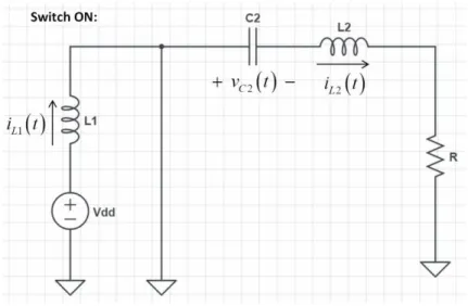
Fig. 2.7 shows the schematic of this model where the constant-current source 𝐼𝐷𝐶 is now
replaced with an RF choke inductor 𝐿1. The unknown state-variables of interest in this case are 𝑖𝐿2(𝑡), 𝑣𝐶2(𝑡), 𝑣𝐶1(𝑡) and 𝑖𝐿1(𝑡).
Fig. 2.7 – Amplifier model 2 schematic. The previous ideal constant-current source assumption in model 1 is now replaced by an RF choke inductor assumption at the drain of the amplifier. Again,
an ideal, lossless switch is considered in place of the transistor.
Including this inductor inherently increases the order and therefore the mathematical complexity of the model. But this can be reduced by expressing the current through the inductor 𝐿1 (𝑖𝐿1(𝑡)) as a linear expression as follows:
𝑖𝐿1(𝑡) = 𝑎𝑡 + 𝑏 (2.62)
This assumption/approximation for 𝑖𝐿1(𝑡) is not arbitrary. Running simulations in ADS2016
(Advanced Design System, Keysight, Santa Rosa, CA) for this model result in a waveform shape as shown in Fig. 4.3 (b). Such a higher order waveform can be approximated by a linear ramp
24
function (equation (2.62)) for a large value of inductor L1, thereby reducing the overall
complexity of the model to second-order. The slope ‘𝑎’ and the y-intercept ‘𝑏’ are calculated and updated during each iteration of the switch operation for both switch-on and switch-off cases as will be shown in the following subsections.
Let’s start our analysis for this model with the switch-on case as follows.
2.5.2.1 Switch-On Case:
Fig. 2.8 shows the schematic for the switch-on case for the amplifier model 2.
Fig. 2.8 – The schematic diagram for the switch-on case of the amplifier model 2
As can be observed from Fig. 2.1, the right side of the circuit is source-free similar to the switch-on case circuit for model 1, meaning its analysis will be identical to the analysis done in Subsection 2.5.1.1. In addition, from the left side of the circuit, we can write the following:
𝑉𝐷𝐷− 0 = 𝐿1𝑑𝑖𝐿1(𝑡) 𝑑𝑡 (2.63) ⇒ 𝑑𝑖𝐿1(𝑡) 𝑑𝑡 = 𝑉𝐷𝐷 𝐿1 (2.64)
Combining (2.11), (2.13), and (2.14) from Subsection 2.5.1.1 with (2.64) above, we can write the state-space matrix representation for the switch-on case of model 2 as follows:
25 𝑑 𝑑𝑡 [ 𝑖𝐿2(𝑡) 𝑣𝐶2(𝑡) 𝑣𝐶1(𝑡) 𝑖𝐿1(𝑡) ] = [ − 𝑅 𝐿2 − 1 𝐿2 0 0 1 𝐶2 0 0 0 0 0 0 0 0 0 0 0] [ 𝑖𝐿2(𝑡) 𝑣𝐶2(𝑡) 𝑣𝐶1(𝑡) 𝑖𝐿1(𝑡) ] + [ 0 0 0 1 𝐿1] 𝑉𝐷𝐷 (2.65)
The expressions for 𝑖𝐿2(𝑡), 𝑣𝐶2(𝑡) and 𝑣𝐶1(𝑡) in this case are exactly the same as derived in Subsection 2.5.1.1, and are summarized as follows:
𝑖𝐿2(𝑡) = 𝐴exp(𝛼𝑡) sin(𝜔𝑑𝑡 + 𝜃) (2.66)
𝑣𝐶2(𝑡) = −(𝑅 + 𝛼𝐿2)𝑖𝐿2(𝑡) − 𝜔𝑑𝐴𝐿2exp(𝛼𝑡) cos(𝜔𝑑𝑡 + 𝜃) (2.67)
𝑣𝐶1(𝑡) = 0 (2.68)
where 𝛼 is the damping coefficient and is defined in (2.27), 𝜔𝑑 is the damped natural frequency and is defined in (2.28), and 𝐴 and 𝜃 are the initial condition constants and are defined in (2.30) and (2.33) respectively.
Finally, let’s derive the expression for 𝑖𝐿1(𝑡). Taking the integral on both sides of (2.64) from
time 0 (the instant the transistor was switched on) to any time t during switch-on, we get:
𝑖𝐿1(𝑡) = 𝑉𝐷𝐷
𝐿1 𝑡 + 𝑖𝐿1(0) (2.69)
where 𝑖𝐿1(0) is an initial condition constant. By comparing the above equation with (2.62),
we get 𝑎 =𝑉𝐷𝐷
𝐿1 and 𝑏 = 𝑖𝐿1(0). The value for b (or equivalently 𝑖𝐿1(0)) can be assigned arbitrarily for the first iteration of the model and then needs to be updated during each iteration.
26
2.5.2.2 Switch-Off Case:
Fig. 2.9 shows the schematic for the switch-off case for the amplifier model 2.
Fig. 2.9 – The schematic diagram for the switch-off case of the amplifier model 2
By using Kirchhoff’s Voltage Law (KVL) and by following the same steps as in Subsection 2.5.1.2, we can write: 𝑑𝑖𝐿2(𝑡) 𝑑𝑡 = − 𝑅 𝐿2𝑖𝐿2(𝑡) − 1 𝐿2𝑣𝐶2(𝑡) + 1 𝐿2𝑣𝐶1(𝑡) (2.70) 𝑑𝑣𝐶2(𝑡) 𝑑𝑡 = 1 𝐶2𝑖𝐿2(𝑡) (2.71)
Now, by Kirchhoff’s Current Law (KCL), we can write:
𝑖𝐶1(𝑡) = 𝐶1 𝑑𝑣𝐶1(𝑡) 𝑑𝑡 = 𝑖𝐿1(𝑡) − 𝑖𝐿2(𝑡) (2.72) ⇒ 𝑑𝑣𝐶1(𝑡) 𝑑𝑡 = − 1 𝐶1𝑖𝐿2(𝑡) + 1 𝐶1𝑖𝐿1(𝑡) (2.73)
Also, we can see from the circuit in Fig. 2.9 that:
𝑉𝐷𝐷 − 𝑣𝐶1(𝑡) = 𝐿1𝑑𝑖𝐿1(𝑡)
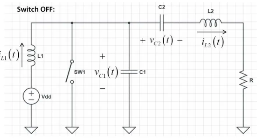
![Fig. 3.1 – The effects of adjusting the load network components on the switch-voltage waveform [35]](https://thumb-eu.123doks.com/thumbv2/9libnet/5762421.116615/51.918.190.763.733.998/fig-effects-adjusting-network-components-switch-voltage-waveform.webp)


![Fig. 3.6 – The block diagram showing different components of the 3-stage driver circuit [2, 3]](https://thumb-eu.123doks.com/thumbv2/9libnet/5762421.116615/67.918.202.775.120.606/block-diagram-showing-different-components-stage-driver-circuit.webp)

