A THESIS SUBMITTED TO
THE GRADUATE SCHOOL OF ENGINNERING AND SCIENCE OF BILKENT UNIVERSITY
IN PARTIAL FULFILLMENT OF THE REQUIREMENTS FOR THE DEGREE OF
MASTER OF SCIENCE IN
MECHANICAL ENGINEERING
By
Mustafa Çağatay Karakan January 2017
ii
DEVELOPMENT OF NANOELECTROMECHANICAL SYSTEMS
FUNCTIONALIZED BY VACUUM ORGANIC THERMAL
EVAPORATION AND THEIR GAS SENSING APPLICATIONS
By Mustafa Çağatay Karakan
January 2017
We certify that we have read this thesis and that in our opinion it is fully adequate, in scope and in quality, as a thesis for the degree of Master of Science.
Mehmet Selim Hanay (Advisor)
Mehmet Zeyyad Baykara
Erdem Alaca
Approved for the Graduate School of Engineering and Science:
Ezhan Karaşan
iii
ABSTRACT
DEVELOPMENT OF NANOELECTROMECHANICAL
SYSTEMS FUNCTIONALIZED BY VACUUM ORGANIC
THERMAL EVAPORATION AND THEIR GAS SENSING
APPLICATIONS
Mustafa Çagatay Karakan M.S. in Mechanical EngineeringAdvisor: Mehmet Selim Hanay January, 2017
Nanoelectromechanical systems (NEMS) are an exquisite sensor technology which is also potentially low-cost since it can be measured electronically and large scale produced using semiconductor fabrication techniques. Since they are extremely sensitive due to their miniscule dimensions and respond very fast due to their high resonance frequencies, these systems can be used as novel mass sensors or gas detectors. However, a functional polymeric layer that is selective to the analyte of interest is required to allow recognition by these sensors and use them as gas concentration detectors.
This work focuses on fabrication of high frequency NEMS resonators, their chemical functionalization and gas sensing applications. Nanomechanical resonators with fully integrated transduction capabilities are fabricated in collaboration with Sabanci University, by using electron-beam lithography and reactive ion etching techniques. Representative micro gas chromatography columns are fabricated by utilizing deep reactive ion etching process. By employing an electronic circuit and downmixing technique, resonant responses of these sensors are measured. First five mechanical modes are observed in open-loop sweeps and up to two modes were tracked
iv
simultaneously by implementing a phase locked loop circuitry. Sub-attogram (10-18 g)
mass sensitivity is achieved under ambient conditions.
Different approaches were adopted for depositing polymer on NEMS and vacuum organic thermal evaporation was chosen due to its repeatability. Effects of functionalization process and thickness of the polymeric film on nanomechanical resonators are analyzed and negligible downgrade on performance of nanomechanical sensors is observed with this technique.
A gas bubbler based vapor generation system was constructed and a microliter chamber for nanomechanical resonators is developed to generate and deliver volatile organic compounds at various concentrations to NEMS sensors functionalized by vacuum organic thermal evaporation. Initially adsorption of water-vapor and subsequent desorption from the sensor surface are successfully observed by tracking the frequency shift via open and closed loops. Then, isopropanol alcohol is used as a test gas and detected by NEMS resonators functionalized with poly (4-vinylphenol). Linear relationship between gas concentration and resulting frequency shift is observed. Finally, possible improvements to enhance selectivity of the NEMS sensor and allow faster recognition are discussed.
Keywords: Nanoelectromechanical systems (NEMS), gas detectors, chemical
v
ÖZET
VAKUM ORGANİK ISISAL BUHARLAŞTIRMA İLE
FONKSİYONELLEŞTİRİLMİŞ NANOELEKTROMEKANİK
SİSTEMLER VE GAZ ÖLÇÜM UYGULAMALARI
Mustafa Çagatay KarakanMakine Mühendisliği, Yüksek Lisans Tez Danışmanı: Mehmet Selim Hanay
Ocak, 2017
Nanoelektromekanik sistemler (NEMS), elektronik olarak ölçülebilen ve yarı iletken üretim teknikleri kullanılarak büyük ölçekli üretilebilen potansiyel olarak düşük maliyetli olan hassas bir sensör teknolojisidir. Nanometre mertebesinde boyutları nedeniyle aşırı duyarlı oldukları ve yüksek rezonans frekansları nedeniyle çok hızlı tepki gösterdikleri için, bu sistemler çok hassas kütle sensörleri veya gaz dedektörleri olarak kullanılabilir. Bununla birlikte, bu algılayıcılar tarafından tanınmayı sağlamak ve bunları gaz konsantrasyon detektörleri olarak kullanmak için, ilgilenilen gaz molekülleri için seçici olan işlevsel bir polimerik katman gerekir.
Bu çalışma, yüksek frekanslı NEMS rezonatörlerinin üretimi, kimyasal işlevselleştirmesi ve gaz algılama uygulamaları üzerine odaklanmaktadır. Nanomekanik rezonatörler Sabancı Üniversitesi işbirliğiyle ve elektron demet litografisi ve reaktif iyon aşındırması yöntemleri kullanılarak üretilmiştir. Sensörlerin hareketi özel tasarlanan bir elektronik devre ve frekans çaprazlama yöntemiyle elektronik bir şekilde ölçülmüştür. Atmosferik koşullarda ilk beş mekanik mod gözlenmiştir ve ve sensor uygulamaları için iki mod aynı anda faz kilitli döngü tarafından takip edilmiştir.
vi
Polimeri NEMS üzerine kaplamak için farklı yaklaşımlar benimsenmiş ve tekrarlanabilirliği nedeniyle vakum organik termal buharlaştırma seçilmiştir. Nanomekanik rezonatörlerin polimerik filmler ile işlevselleştirme prosesininde oluşan film kalınlığı ve filmin sensorün performansı üzerindeki etkisi analiz edilmiş ve bu metodun hassas nanomekanik sensörleri fonksiyonel hale getirmek için uygun olduğu görülmüştür.
Vakum organik termal buharlaştırma ile işlevselleştirilen NEMS algılayıcılarına çeşitli konsantrasyonlarda uçucu organik bileşikler üretmek ve iletmek için bir gaz manifoldu kurulmuş ve sensörler için mikrolitre hacminde bir hazne geliştirilmiştir. İlk olarak algılayıcı yüzeyinin su buharı soğurduğu ve bu moleküllerin kuru azot kullanılarak yüzeyden salındığı başarıyla gözlenlenmiştir. Sonrasında izopropil alkol deneylerde test gazı olarak kullanmış ve polivinilfenol ile fonksiyonelleştirilmiş nanomekanik rezonatörler ile farklı konsantrasyonlarda tespit edilmiş, gaz konsantrasyonu ile sensördeki frekans kayması arasında lineer bir ilişki olduğu gözlemlenmiştir. Son olarak sensörün seçiciliğini ve algılama hızını artırmak için uygulanabilecek geliştirmeler belirtilmişir.
Anahtar kelimeler: Nanoelektromekanik sistemler (NEMS), gaz dedektörü, kimyasal
vii
Contents
1 Introduction ... 1
1.1 Nanoelectromechanical Systems (NEMS) ... 1
1.2 NEMS as Gas Detectors ... 3
1.3 Micro Gas Chromatograph ... 6
1.4 Motivation and Outline ... 6
2 Development of NEMS Devices ... 8
2.1 Transduction Principle for NEMS ... 8
2.2 Fabrication of Nanomechanical Resonators ... 9
2.2.1 Fabrication of Micro Gas Chromatograph Columns ... 15
2.3 Electronic Measurement of Nanomechanical Resonators by Signal Downmixing ... 21
2.3.1 Phase Locked Loop ... 26
3 Functionalization of NEMS Devices with Polymeric Thin Films ... 29
3.1 Solvent Based Drop Casting ... 29
3.2 Vacuum Organic Thermal Evaporation ... 32
4 Gas Sensing Experiment ... 41
4.1 Gas Manifold ... 41
4.2 Sensor Chamber ... 44
4.3 Functionalized NEMS as a Detector ... 47
5 Conclusion and Future Work ... 54
5.1 Conclusion ... 54
5.2 Future Work ... 55
5.2.1 Permeation Tubes ... 56
viii
List of Figures
Figure 1.1: One of the first examples of a nanomechanical resonator [2] ... 2
Figure 1.2: NEMS and analysis at molecular level [10] ... 3
Figure 1.3: An illustration of adsorption of vapor from gas phase to polymer phase [18] ... 4
Figure 1.4: Identification of chemical warfare agents with polymer coated NEMS [19] ... 5
Figure 1.5: An illustration of a NEMS based electronic nose for early diagnosis from breath samples... 7
Figure 2.1: Modeshapes of first (a) and second (b) flexural modes and their corresponding elastic strain energy density. ... 9
Figure 2.2: Schematic from mask layout designed for fabrication process. ... 10
Figure 2.3: Fabrication scheme. (b), (c) and (d) represents the resulting cross section after third, fourth and sixth steps respectively ... 11
Figure 2.4: Optical and SEM figures from sample after finishing fabrication procedure. ... 13
Figure 2.5: Interconnections between NEMS and printed circuit board ... 14
Figure 2.6: Mask design for micro chromatograph columns with a channel length of 20 µm and total length of 100 cm. ... 15
Figure 2.7: Fabrication scheme for the fabrication of micro gas chromatograph columns. ... 17
Figure 2.8: Standard and alternative micro gas chromatograph chips after completing the fabrication procedure. ... 19
Figure 2.9: SEM micrograph from 25mm x 25mm µGC chip... 20
Figure 2.10: SEM micrograph from 12mm x 15mm µGC chip... 20
Figure 2.11: Simplified DBOX architecture ... 21
ix
Figure 2.13: DBOX and Electronic measurement setup, NEMS chip on a printed circuit board and a typical NEMS resonance curve (to ensure that signal has a mechanical origin, resonance is driven to nonlinear regime). ... 23 Figure 2.14: a) Resonant response of first two modes of a NEMS sensor (6µm x 320nm x 100nm). ... 23 Figure 2.15: Frequency vs. Amplitude graph of first five modes for longer device (10µm x 950nm x 100nm) ... 25 Figure 2.16: Quality factor for fist five modes– as expected from viscous damping, quality factor increases with 𝑓 in air. ... 25 Figure 2.17: Amplitude-Phase vs Frequency curve of one of our nanomechanical resonators, bandwidth of the response is represented by red lines and phase at the peak amplitude is represented by an orange dot. ... 27 Figure 2.18: Allan deviation of a nanomechanical resonator. PLL settling time is around 0.5s and Allan deviation is around 2 parts-per-million. ... 28 Figure 2.19: Simultanious measurement of two modes of a NEMS sensor. At two instances, water-vapor is sent to the system and resulting downshift can be observed. ... 28 Figure 3.1: SEM micrographs of doubly clamped beam after dropcasting process. . 31 Figure 3.2: SEM micrographs after drop casting polymers on doubly clamped beams at higher concentration... 31 Figure 3.3: a) Organic Thin Film Evaporator at UNAM facility. b) Crucible and resistance heater ... 33 Figure 3.4: Micrographs (a, b) and surface profile (c) of a partially masked silicon nitride chip. Red dashed lines represent scan direction for profilometer ... 34 Figure 3.5: SEM micrographs of a nanomechanical resonator before and after thermal evaporation of PVPh. Scale bar is 500nm. ... 34 Figure 3.6: Frequency shifts on 1st and 2nd mode after vacuum thermal evaporation of PVPh. ... 35 Figure 3.7: Frequency shift on the first mode after repeating vacuum thermal organic evaporation of PVPh. ... 36
x
Figure 3.8: Optical microscopy image of wirebonded multimode NEMS after functionalization process. ... 37 Figure 3.9: Long range frequency sweep before and after vacuum thermal organic evaporation of PVPh ... 38 Figure 3.10: Real (red) and imaginary (blue) quadratures of first four modes before (left) and after (right) functionalization process. ... 39 Figure 3.11: Images taken with optical microscopy and SEM after vacuum thermal evaporation of PMMA on partially masked silicon nitride chip. ... 40 Figure 4.1: Gas manifold and its elements: Mass Flow Controllers, solenoid valves and gas bubblers (from left to right) ... 42 Figure 4.2: Operating principle of a gas bubbler and a picture of gas bubbler that is used in experiments ... 43 Figure 4.3: High volume chamber for gas sensing experiments. ... 44 Figure 4.4: Experiments with water-vapor. Water-vapor with the concentration of 17ppth induced (solenoid is opened) between 500-560s, 650-670s, 760-790s and 1100 – 1500s. ... 45 Figure 4.5: Microliter chamber ... 46 Figure 4.6: Gas manifold under fume hood (a) and reduction scheme from stainless steel pipe to capillary tube (b)... 46 Figure 4.7: Resonant response of NEMS sensor before and after sealing of microfluidic chamber ... 47 Figure 4.8: Desorption of molecules from surface of NEMS sensor following a nitrogen purge ... 48 Figure 4.9: NEMS response under nitrogen flow. ... 49 Figure 4.10: Testing 1-iodononane and Decanal on Polyvinylphenol coated NEMS. Even though sensor is exposed to cancer biomarkers in marked area, we could not observe a distinctive shift on resonance frequency of NEMS sensors. ... 50 Figure 4.11: Gas sensing experiments with IPA. ... 51 Figure 4.12: Detection of IPA at various concentrations with PVPh coated NEMS. 52 Figure 4.13: Frequency shift of PVPh coated NEMS under different concentrations of IPA ... 53
xi
xii
List of Tables
Table 2.1: Dimensions of the designed NEMS structure. ... 10
Table 2.2: Process parameters for plasma etching ... 13
Table 2.3: Dimensions of micro gas chromatograph columns ... 15
Table 2.4: Recipe for deep reactive ion etching process ... 18
Table 2.5: Resonance frequencies of simulated and experimental modes and their quality factors ... 26
xiii
Acknowledgement
First of all, I would like to express my profound gratitude to my dear academic advisor Prof. Mehmet Selim Hanay for his generous and unlimited support, guidance and patience throughout my graduate study and dissertation period. He is probably the best professor a graduate student can have.
I want to thank my thesis committee, Prof. Erdem Alaca and Prof. Mehmet Zeyyad Baykara for their time and valuable suggestions.
I want to thank my dear friends and members of our research group; Atakan Arı, Mehmet Kelleci, Selçuk Oğuz Erbil, Ezgi Orhan, Hande Aydoğmuş, Levent Aslanbaş, Mert Yüksel and Arda Seçme for all ideas, discussions and fun times we had. Atakan has been my partner in crime in research since the first day of graduate study, I feel lucky to have worked with him, NEMS resonators and gas chromatograph columns fabricated in this work are made possible with his outstanding nanofabrication skills. Besides, I am grateful to Mehmet and Selçuk for their support and practical solutions about gas manifold. I want to thank Dr. Daryoush Majidi for all of his contributions during our project. Your friendships have made the lab and my time here much more fun and memorable.
I want to acknowledge Dr. Cenk Yanık and Prof. Ismet Inonü Kaya for their support and collaboration. I would like to also thank technical staff of UNAM for their support in our projects.
Last but definitely not the least, I wish to thank my family: Ayşe, Mehmet, Önder and Alican for their unconditional love, support and continious encouragement throughout my life.
I gratefully acknowledge support by Scientific and Technical Council of Turkey (TUBITAK), Project No: 213E036.
1
1 Introduction
In the modern world, nanotechnology has become an important part of daily lives even if our eyes are not able to realize it. Personal computers, smartphones operate based on millions to few billions of transistors packaged inside. A decent smartphone also includes many integrated sensors within, which are able to detect heart rate, fingerprint, light, proximity, pressure, orientation, location and so on. These products are commercially available 50 years after the inspiring talk of Nobel laureate Richard Feynman [1] about miniaturization. Starting from early 1980’s, semiconductor based microfabrication techniques have emerged and rapidly developed over the last decades. This miniaturization is ingeniously utilized by researchers and engineers to develop tiny mechanical devices that are controlled electrically. These devices are known as microelectromechanical systems or MEMS. Over the years, nanofabrication techniques further evolved and development of devices in nanometer scale was made possible.
1.1 Nanoelectromechanical Systems (NEMS)
Nanoelectromechanical Systems (NEMS) are electronically controlled mechanical devices with at least one dimension smaller than 1 micrometer. First examples of NEMS devices are demonstrated by Cleland & Roukes in 1996 [2]. Since then, it is an active and emergent field of research, NEMS circuits are widely used as a probe for fundamental physics studies, such as approaching quantum limit [3], nanoscale displacement sensing [4] and preparation of ultracold states [5]; as well as biological [6] and chemical sensing applications [7]. Recently, NEMS technology are being developed at academic laboratories and microelectronic manufacturing and test centers. Owing to rapid advancements in nanofabrication technology, it is now
2
possible to produce thousands of NEMS devices by a single fabrication procedure and use them in scientific research, as well as real life applications [8].
Figure 1.1: One of the first examples of a nanomechanical resonator [2]
One of the important applications of NEMS technology is the measurement of miniscule masses. NEMS devices can measure mass at molecular level and identify an unknown sample at this point. The use of a NEMS device as a mass sensor is based on measuring resonance frequency of mechanical structure. The frequency of any mechanical vibration mode of a NEMS structure depends on its effective spring constant and mass of that vibration mode.
In mass sensing experiments, these vibrational frequencies are typically monitored by an electronic circuit. At this time, molecules of the analyte to be investigated are sent over this NEMS structure and as each molecule is absorbed one by one on the surface, distinct changes in the resonance frequencies of the NEMS device are observed (as in Figure 1.2). Each sharp shift is caused by the landing of a single molecule on the device, and the magnitude of the frequency change is directly proportional to the mass of this molecule. Resulting shift 𝛥𝑓𝑛𝑒𝑚𝑠 on resonance frequency 𝑓𝑛𝑒𝑚𝑠 caused by the added mass 𝛥𝑚 can be expressed by the equation below [9]:
3 𝛥𝑓𝑛𝑒𝑚𝑠 = −1
2 𝑓𝑛𝑒𝑚𝑠
𝑀𝑛𝑒𝑚𝑠 𝛥𝑚 (1.1)
Figure 1.2: NEMS and analysis at molecular level [10]
Nanomechanical mass measurement experiments have been extensively studied during the last decade. Mass resolution at attogram (10-18 g) using NEMS was first
demonstrated in 2004 [11]. Over the years, various samples were examined with this level of sensitivity in [12] and [13]. Mass resolution with zeptogram (10-21 g) with
NEMS circuits was reached in 2006 [14]. These circuits were devices that are produced by top-down fabrication techniques. On the other hand, carbon nanotube based devices that are developed by bottom up fabrication techniques are demonstrated by Chiu et al. [15] in 2008. The first NEMS mass spectrometry examining protein samples was first demonstrated in 2009 [10]. At 2012, atomic mass resolution at yoctogram (10-24
g) is achieved by using carbon nanotube based devices which have extremely low effective mass [16]. Using NEMS structures, real-time mass spectrometry of single protein molecules is demonstrated by Hanay et al. in 2012 [17].
1.2 NEMS as Gas Detectors
Nanoelectromechanical systems can be used for chemical sensing applications. In order to accomplish that, modification of the sensor surface with a functional material
4
is required to allow adsorption of analyte of interest by the sensor surface. For vapor sensing applications, polymer films are usually used as a functional material to form an active layer on the surface of NEMS. The first step in measuring a gas concentration by NEMS is the adsorption of a fraction of these of molecules in the gas phase by the polymeric film. In this step, there is a thermodynamic equilibrium between the concentration of the chemical in gas phase and the concentration of the chemical in polymer phase. An illustration demonstrating this equilibrium is shown in Figure 1.3 and a parameter representing the equilibrium as the ratio of the concentration in sorbed phase over gas phase is called as partition coefficient (K). Partition coefficient is typically different for each analyte-polymer pair and it is one of the most important factors that determine sensitivity and selectivity of the sensor.
Figure 1.3: An illustration of adsorption of vapor from gas phase to polymer phase [18]
Depending on the partition coefficient, a fraction of these molecules are diffused into the polymeric layer on NEMS and increases the total mass of the resonator. Mass adsorbed by this functional layer can be defined as:
𝛥𝑚 = 𝐾𝑉𝑝𝐶𝑠 (1.2)
Where 𝑉𝑝 is the volume of polymer layer and 𝐶𝑠 is the concentration of analyte in sorbed phase. By combining with Eq. 1.1, resulting frequency shift can be defined as follows:
5 𝛥𝑓𝑛𝑒𝑚𝑠 = −1
2 𝑓𝑛𝑒𝑚𝑠
𝑀𝑛𝑒𝑚𝑠 𝐾𝑉𝑝𝐶𝑠 (1.3)
By using NEMS devices functionalized with polymeric films, various chemical gases are detected at parts-per-billion concentrations in 2010 by Li et al. [19]. In this work, two NEMS resonators are functionalized by two different polymers and integrated with a gas chromatography system (Figure 1.4). With this technique, they were able to detect a dozen of chemical compounds in vapor phase. Recently, more sensitive methods are developed to functionalize NEMS sensors, such as surface initiated polymerization of monomers on the detector substrate by McCaig et al. [20].
.
Figure 1.4: Identification of chemical warfare agents with polymer coated NEMS [19]
Figure 1.4 demonstrates the ability of NEMS technology to detect gas molecules. In the figure on the left, various organic gases and chemical warfare agents are detected at the same time with both NEMS (top) and the flame ionization detector (bottom). The vertical axis shows the NEMS signal (frequency shift, blue color) and the amount of ionic current (pink color). Only one NEMS and one polymer were used for the figure in the left. Therefore, some chemicals (such as Toluene and Octane) were could not be detected due to the low partition coefficients between polymer that is used in this work and gas molecules. The figure on the right demonstrates an identification of gas molecules by using two NEMS circuits, a polymer and a gas chromatograph. In this case, the data obtained are of three dimensions (two polymers + NEMS arrival time) and allowed for more precise classification of these chemicals.
6
1.3 Micro Gas Chromatograph
Miniaturization of gas chromatograph system on Silicon chips is first introduced towards the end of 1970’s [21]. In these initial systems, stationary phase is injected towards the chromaograph after the fabrication process and resulted with an inhomogenous sorption region. This limitation has been overcome at mid 1990’s by integrating stationary phase creation to the microfabrication process [22]. As MEMS and lab-on-a-chip technology rapidly developed after 2000s, miniaturation of gas chromatograph columns is further advanced and subsystems such as preconcentrators and heaters are integrated and manufactured on chip [23-25]. Micro gas chromatographs that seperate organic compounds at parts-per-billion level have been demonstrated in 2009 and 2011 [26, 27]. By using optical lithography and plasma etching methods, it is possible to manufacture micro gas chromatograph columns with micrometer sized column width and 1 meter in length. In this thesis, fabrication of representative micro gas chromatopgraph columns are demonstrated in Chapter 2.
1.4 Motivation and Outline
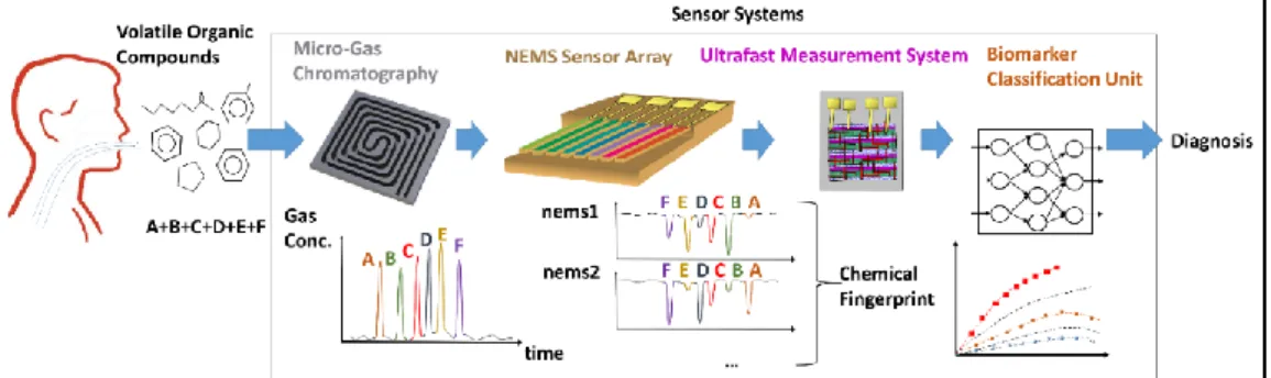
As demonstrated by Figure 1.4, NEMS resonators can respond very quickly due to their high resonance frequencies. By integrating a micro gas chromatograph that seperates individual components in time and NEMS sensors coated with different polymers, a chip scale total gas analysis system that is able to identify individual components can be developed. This type of system can be used in various applications, such as detection of cancer biomarkers from human breath [28]. Signal flow from that kind of system is shown in Figure 1.5.
This thesis focuses on development of nanoelectromechanical systems, their chemical functionalization by vacuum organic thermal evaporation and gas sensing applications.
7
Figure 1.5: An illustration of a NEMS based electronic nose for early diagnosis from breath samples
In this introductory Chapter 1, Nanoelectromechanical systems, their mass sensing and chemical gas sensing mechanism and capabilities are described.
Chapter 2 starts with fabrication of multimode NEMS devices and micro gas chromatograph columns. A fully electronic actuation and detection scheme based on signal downmixing is then described, measurement of NEMS resonators and detection of up to five mechanical modes are shown. Resonance frequencies of resonators are tracked by employing a phase locked loop to use them in gas sensing applications.
In Chapter 3, functionalization of NEMS sensors are described. Solvent based dropcasting and vacuum organic thermal evaporation techniques are employed as functionalization methods. Vacuum organic thermal evaporation method is preferred due to its high reprocibility. Effects of this functionalization process on NEMS sensors and their quality factors are analyzed.
In Chapter 4, a gas manifold that can generate tunable concentration of volatile organic compounds is described initially. Gas sensing measurements with NEMS sensors functionalized by vacuum organic thermal evaporation are shown.
Chapter 5 provides a general summary of this M.S. thesis and discusses possible improvements.
8
2 Development of NEMS Devices
2.1 Transduction Principle for NEMS
Througout this thesis, nanomechanical resonators are designed as silicon nitride doubly clamped beams for robustness and preventing possible stiction problems. Transduction in NEMS is enabled by integrating gold electrodes near clampling region, which provides thermoelastic actuation and geometric piezoresistivity for detection [17], [29].
In our design, applying a voltage through one U - shaped gold electrode generates local Joule heating through a metallic loop on the one end of the doubly clamped beam. Since gold electrode and and silicon nitride substrate have different coefficients of linear thermal expansion (𝛼𝐴𝑢≈ 14 𝑥 10−6,𝛼𝑆𝑖𝑁 ≈ 3.3 𝑥 10−6), strain difference
between two layers bends bilayer NEMS structure. By alternating the temperature periodically at the resonance frequency of doubly clamped beam, we enabled actuation of nanomechanical resonator.
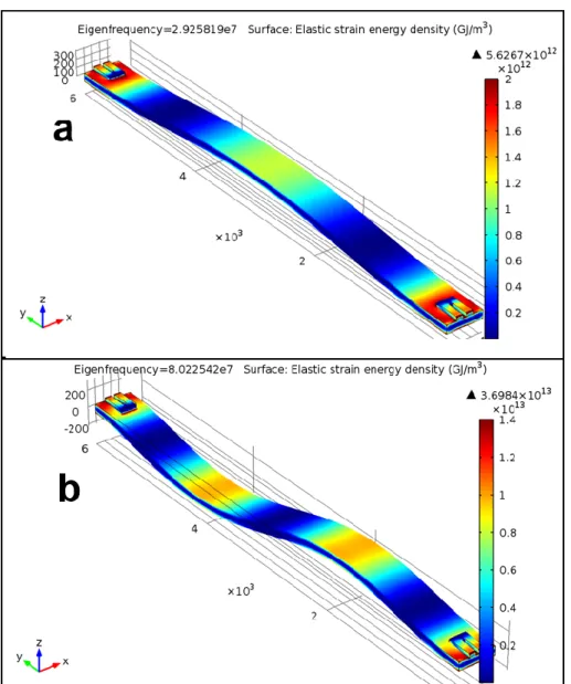
When device is in motion, gold electrode integrated on the other end of the beam also deforms due to applied stress. This in turn changes the geometry of the gold electrode which results with a variation of ΔR in its resistance during motion. When device undergoes motion, strain energy grows particularly at clamping regions as indicated by Figure 2.1 and piezoresistive transduction efficiency of the gold electrode increases when a mechanical mode is excited.
9
Figure 2.1: Modeshapes of first (a) and second (b) flexural modes and their corresponding elastic strain energy density.
2.2 Fabrication of Nanomechanical Resonators
Throughout this thesis, NEMS structures are fabricated by using micro/nano fabrication techniques.
10
Figure 2.2: Schematic from mask layout designed for fabrication process.
Figure 2.2 represents the design for 9mm x 9mm chip. Contact pads, length indicators for doubly clamped beams and alignment markers to ensure proper adjustment between different layers can be observed from Figure 2.2(a). NEMS area that contains four doubly clamped beams is shown in Figure 2.2(b); an individual beam together with the transduction electrodes is shown in Figure 2.2(c). Dimensions of NEMS structures as we designed are shown below in Table 2.1.
Table 2.1: Dimensions of the designed NEMS structure. Dimensions of NEMS structures Length 4 µm – 5µm - 6 µm – 8 µm Width 360 nm Thickness 100 nm Electrode length 500 nm Electrode width 80 nm Spacing between electrode legs 80 nm
11
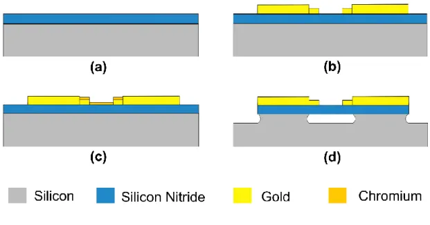
Nanofabrication processes are performed at National Nanotechnology Research Center (UNAM) and Sabancı University Nanotechnology Research and Application Center (SUNUM). In order to achieve desired resolution and alignment accuracy, high resolution electron – beam lithography system (Vistec / EBPG5000plusES) is utilized with the expertise of Dr. Cenk Yanik and Prof. Dr. Ismet Inonu Kaya. For etching process, Inductively Coupled Plasma (SRTS) system within the cleanroom facility of UNAM is used. A simplified version of the fabrication scheme is shown below in Figure 2.3.
Figure 2.3: Fabrication scheme. (b), (c) and (d) represents the resulting cross section after third, fourth and sixth steps respectively
Fabrication Scheme:
1) A silicon chip (9 mm x 9 mm) with 100 nm LPCVD grown low stress Silicon Nitride (obtained from University Wafer) on top is cleaned using Acetone, Isopropanol Alcohol and DI water.
2) On the substrate, bilayer PMMA 495 A4 and PMMA 950 A2 (MicroChem) are spin coated as electron beam resist. Gold electrodes on nanomechanical resonators and
12
alignment markers for the next step are patterned with electron-beam lithography. After development, 60 nm gold layer with a 3 nm chromium adhesion layer is deposited by thermal evaporation and residuals are lifted off by acetone.
3) After another step of PMMA spin coating and aligment, second electron beam lithography step is performed to define 200 µm square shaped contact pads. Subsequently 3 nm chromium and a thicker gold layer (100 nm) is thermally evaporated and lifted off.
4) Following the same procedure and careful aligment, third electron beam lithography step is performed to define the dimensions of nanomechanical structure. After exposure and development, 60 nm chromium is thermally evaporated to be served as an etch mask and lifted off.
5) Silicon Nitride (SiN) device layer is suspended from the substrate with two steps of plasma etching. Initially, chip is cleaned with oxygen plasma and chamber is conditioned by applying recipe to the empty chamber. At the first step, SiN layer apart from masked chromium layer is anisotropically etched by a recipe based on tetrafluoromethane and fluoroform (CF4 / CHF3) based plasma. Silicon layer beneath
the NEMS structure is then isotropically etched with a sulfur hexafluoride and fluoroform (SF6 / CHF3) plasma to release the nanomechanical structure.
6) Remaining chromium etch mask on device is removed with another plasma etching procedure. Chlorine and oxygen (Cl2 / O2) plasma is generated to etch the chromium
13
Table 2.2: Process parameters for plasma etching Etch process
parameters
Anisotropic SiN etch (for 100 nm thickness)
Isotropic Si etch (to release 400 nm width
beam) Chromium Removal (for 60nm thickness) Plasma and flow rate 20 sscm CF4 , 3 sscm CHF3 45 sscm SF6, 20sscm CHF3 24 sscm Cl2 , 6 sscm O2
Pressure 5 mTorr 10 mTorr 5 mTorr
Coil Power 400W 400 W 600 W
Platen
Power 100 W 100 W 50 W
Time 1 minute 1 minute 2 minutes
After completing fabrication procedure, devices are investigated under optical and scanning electron microscope (SEM) before electronic measurement to ensure alignment between gold electrodes and doubly clamped beam, suspension of the NEMS structure and removal of chromium layer. Results can be seen from the figure below.
Figure 2.4: Optical and SEM figures from sample after finishing fabrication procedure.
14
On Figure 2.4(a); yellow, blue and gray colors represent gold, silicon nitride and silicon substrate underneath respectively. Clear distinction of the colors indicates a successful completion of evaporation and etcing steps. Alignment accuracy and suspension of the beams with minimum undercut are validated by Scanning Electron Microscopy.
After the fabrication process, interconnections between gold contact pads and printed circuit board (PCB) are made by wirebonder (Kulicke & Soffa). This step enabled us to establish a connection between electronic measurement equipment and NEMS device. Since the Gold / Chromium adhesion layer deposited for the contact pads are thinner than expected at the first fabrication trials, some wirebonding processes were repeated to ensure proper connection.
15
2.2.1 Fabrication of Micro Gas Chromatograph Columns
We designed a photomask as a first step for fabrication of micro gas chromatograph columns. A standard and an alternative design is made, where alternative version has a narrower column width and smaller dimensions as a whole chip. Inlet for gas entrance and an outlet is designed for the insertion of fused silica capillary tubes with the dimensions of 360 µm outer diameter 100 µm inner diameter. Sealing of the chip and coating of columns with a passivation layer are not included in this thesis and will be done at future work.Table 2.3: Dimensions of micro gas chromatograph columns Column
Length
Column Width Column Depth Chip
dimensions
Standard 160 cm 100 µm 160 µm 25 mm x 25 mm
Alternative 100 cm 20 µm 160 µm 12 mm x 15mm
Figure 2.6: Mask design for micro chromatograph columns with a channel length of 20 µm and total length of 100 cm.
16
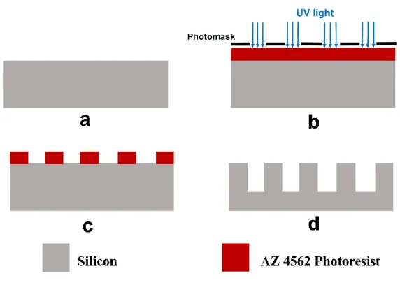
Proposed micro gas chromatograph colmuns are fabricated in UNAM cleanroom environment by using photolithography and deep reactive ion etching (DRIE) process. Fabrication scheme for the process is described in Figure 3 below. By starting with a silicon wafer (University Wafer) and following the recipe, an etch mask is coated on the substrate and subsequently etched with inductively coupled plasma. Recipe is described as below:
1) First step is cleaning the wafer with acetone and isopropanol, then rinsing it with deionized (DI) water. Cleaning process is then repeated after wafer is immersed to buffered oxide etch (1 units of hydrofluoric acid: 7 units of DI water) in order to remove the thin oxide layer on the substrate. Then wafer is baked at 110 ˚C for 2 minutes to remove the moisture on the surface. (Figure 2.7).
2) Hexamethyldisilazane (HMDS) is spin coated at 4000 rpm to promote the adhesion of the photoresist at the next step.
3) AZ 4562 positive thick film resist is spin coated on to the substrate at 2000 rpm for 30 seconds, resulting with a film thickness around 9 µm.
4) After waiting for 3 minutes to eliminate bubble formation due to the solvent trapped inside the photoresist, wafer is baked at 110 ˚C for 90 seconds to evaporate the photoresist solvent.
5) After aligning the photomask, wafer is exposed to UV light under 400mJ /cm2 with
mask aligner (EVG 620) at soft contact mode (Figure 2.7b).
6) Exposed photoresist on the silicon wafer is developed by soaking it to pure AZ400K developer for 40 seconds and rinsing it with DI water. Since we used a pure developer, timing is crucial for this step to prevent any over-developing issue.
7) After drying the sample with nitrogen, wafer is baked at 90 ˚C for 15 minutes to
17
8) Silicon wafer is etched anisotropically by using SF6 based plasma with applied bias
power to obtain high aspect ratio vertical channels for chromatograph columns. C4F8
is used as a passivation layer to prevent excessive etching of etch mask and maintain anisotropic profile. 980 cycles are applied in this process to obtain 160 µm depth for columns.
Figure 2.7: Fabrication scheme for the fabrication of micro gas chromatograph columns.
18
Table 2.4: Recipe for deep reactive ion etching process
Passivation Etching Cycle Time 7s 10s Pressure 20mT 35mT C4F8 Flow 70 sscm - SF6 Flow - 80 sscm O2 Flow - 5 sscm Coil Power 200 W 200 W Bias Power - 13 W Bias Frequency - 13.56 MHz Chinner Temperature 20 ˚C 20 ˚C Heater Temperature - 45 ˚C
Platen Matching Load 35, Tune
50
Load 35, Tune 50
Coil Matcing Load 40, Tune
60
Load 40, Tune 50
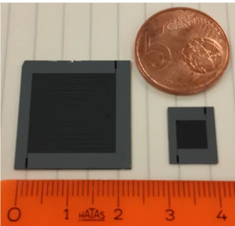
9) Wafer is then diced with a dicing saw (Disco DAD3220) according to the chip dimensions given in Table 2.3, subsequently soaked into the acetone in order to remove the photoresist and clean the surface. A photograph taken after the process is shown below in Figure 2.8. A coin and a metric ruler is included as a scale bar.
19
Figure 2.8: Standard and alternative micro gas chromatograph chips after completing the fabrication procedure.
Scanning Electron Microscope is used to investigate the effect of etching process and characterize dimensions of columns. Inspection of columns and inlets are shown below in Figure 2.9 and Figure 2.10.
20
Figure 2.9: SEM micrograph from 25mm x 25mm µGC chip
While fabricated columns are in a good agreement with the dimensions, stagmite formation at the bottom and a slight isotropy can be observed from Figure 2.10a. We believe that stagmite formation is a residue from C4F8 passivation layer.
21
2.3 Electronic Measurement of Nanomechanical
Resonators by Signal Downmixing
In order to enable transduction for NEMS resonator, an equipment named DBOX (Asgyn) is employed. Simplified architecture of DBOX is shown in Figure 2.11. DBOX contains two synchronized function generators and one digital lock-in amplifier to drive the resonators and measure the output signal.
Figure 2.11: Simplified DBOX architecture
A representative circuit for measurement scheme is shown in Figure 2.12. For actuation of NEMS sensors, an AC drive voltage at the half frequency of the mechanical motion, 𝑉𝑑cos (
𝜔𝑑𝑟𝑖𝑣𝑒
2 ), is applied to the driving electrode. Resulting
temperature modulation on the gold actuation loop drives the doubly clamped beam as explained in Chapter 2.1. Temperature modulation due to joule heating is depending on the power and it is proportional with square of this voltage.
𝑃𝑑𝑟𝑖𝑣𝑒~
𝑉𝑑2
22
Figure 2.12: Actuation and readout scheme for NEMS resonators
For measurement of NEMS sensors, the geometric piezoresistance change of the detection electrode is measured. Downmixing technique is employed to reduce the effect of parasitic capacitances so that the readout signal of mechanical motion, which is in the order of 10-100 MHz, has been reduced to the order of 10-100 kHz (Δω) [30]. This technique also allows the filtering of any high frequency noise sources such as coupling of actuation signal or cable resonances.
To enable downmixing, a signal having a high frequency and slightly different from the drive frequency of the resonator (ω + Δω) is applied to the readout electrode as an AC bias voltage. With this bias voltage, an output signal at frequency Δω arises from the modulation due to the NEMS motion and piezoresistance of the detection electrode. Any other signal is filtered by low pass filter which has a cut-off frequency of 100 kHz.
Mechanical resonances are detected by measuring this downmixed frequency signal in experiments. Actuation is based on thermoelastic mechanism.
The drive and bias voltages used in the experiments are optimized separately for each NEMS sensor and are usually between 10 mV and 100 mV. Applying voltages above 100 mV for the fabricated structures cause the thin gold electrodes to burn or the NEMS sensor to pass through the nonlinear regime (as can be observed from Figure 2.13); whereas applying voltages below 10 mV substantially decreases signal to noise and signal to background ratio of the resonator. The readout signal generated by a NEMS is typically in the range of 1-10 μV and measured by applying 60-84 dB from a low noise amplifier embedded in DBOX.
23
Figure 2.13: DBOX and Electronic measurement setup, NEMS chip on a printed circuit board and a typical NEMS resonance curve (to ensure that signal has a
mechanical origin, resonance is driven to nonlinear regime).
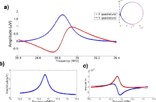
Example results by applying the thermoelastic actuation and mix-down measurement scheme are shown in Figure 2.14. Resonant responses of first two modes are detected with a low signal to noise and signal to background ratio. Lorentzian fits are almost indistinguishable and indicates a quality factor of 150 for the first mode at 28.82 MHz and 230 for the second mode at 71.9 MHz.
Figure 2.14: a) Resonant response of first two modes of a NEMS sensor (6µm x 320nm x 100nm).
24
We were able to detect higher order modes of another device with larger dimensions. First five resonance modes measured for a device of length 10 µm (Figure 2.15). On Figure 2.16, quality factors as a function of frequency is shown. We determined quality factors of these modes by applying a Lorentzian fit and a proportionality of quality factors with √𝑓 is observed, as expected from viscous damping model. These results indicate that using mechanical modes with higher frequencies offer better resolution for sensing applications. By using COMSOL Multiphysics, we performed finite element simulations to obtain theoretical resonance frequencies. Comparison of the experimental resonance frequencies and theoretical ones are shown in Table 2.5.
25
Figure 2.15: Frequency vs. Amplitude graph of first five modes for longer device (10µm x 950nm x 100nm)
Figure 2.16: Quality factor for fist five modes– as expected from viscous damping, quality factor increases with √𝑓 in air.
26
Table 2.5: Resonance frequencies of simulated and experimental modes and their quality factors
Mode
Number FEM (COMSOL) Experimental Quality Factor
1 10.34 MHz 13.88 MHz 104 ± 1 2 28.48 MHz 30.5 MHz 182 ± 2 3 55.79 MHz 50.24 MHz 230 ± 2 4 71.39 MHz (torsional) 71.58 MHz 299 ± 3 5 88.19 MHz (first in-plane) 94.01 MHz 311 ± 6 6 92.17 MHz - - 7 137.59 MHz - -
2.3.1 Phase Locked Loop
Phase locked loop (PLL) is a commonly used closed loop control technique to constantly drive a resonator in its resonance frequency and track it for frequency shift based sensing applications. Phase (∅) is defined as in Eq. 2.2, where 𝑋 and 𝑌 are real and imaginary quadratures of resonant response:
∅ = 𝑎𝑟𝑐𝑡𝑎𝑛(𝑌
𝑋) (2.2)
In phase locked loop circuitry we implemented in this thesis, resonator is driven at its peak amplitude and reference phase at this point is adjusted to zero. Then, phase value is calculated and compared with the reference value with the frequency of the sampling rate of lock-in amplifier. Phase error between the input of voltage controlled oscillator and output of the resonator is kept at zero by a low pass loop filter inside the lock-in amplifier with adjustable gain. Gain is depending on the slope of phase/frequency response of the resonator (i.e. low slope requires higher gain or positive slope requires positive feedback).
27
Figure 2.17: Amplitude-Phase vs Frequency curve of one of our nanomechanical resonators, bandwidth of the response is represented by red lines and phase at the
peak amplitude is represented by an orange dot.
The frequency stability of the NEMS sensor is generally determined by a parameter called Allan Deviation, which can be considered as the ratio of the minimum frequency shift that can be measured to the driving frequency of the resonator. As an example, the Allan deviation plot for a NEMS sensor with a closed loop response time of 500 ms is shown in Figure 2.18. The values calculated with respect to the various integration times demonstrate the stability of the sensor in different timescales. The PLL settling time corresponds to the sensitivity and frequency stability of nanomechanical resonator for sensing applications. The values of the Allan deviation over a longer period of time indicate the effect of long-term drift and deviations below PLL settling time are due to the low-pass filter dynamics in closed-loop transfer function rather than physical perturbations.
28
Figure 2.18: Allan deviation of a nanomechanical resonator. PLL settling time is around 0.5s and Allan deviation is around 2 parts-per-million.
By using different reference downmixing frequencies for two modes (Δω1 and Δω2),
it is possible to track resonance frequencies of two modes simultaneously. An example is shown in Figure 2.19.
Figure 2.19: Simultanious measurement of two modes of a NEMS sensor. At two instances, water-vapor is sent to the system and resulting downshift can be observed.
29
3 Functionalization of NEMS
Devices with Polymeric Thin
Films
Functionalization of the surface for sensors has a vital role for gas sensing applications. For gravimetric sensors, polymers are widely considered as a functional layer to enable the adsorption of the analyte on the surface of nanomechanical sensor. There are several techniques in the literature to accomplish that, including; solvent based drop-casting, spin coating, inkjet printing or self-assembly based bottom-up methods [20]. Among those techniques, we applied solvent based drop casting and organic vacuum thermal evaporation to functionalize the surface of nanomechanical resonators.
3.1 Solvent Based Drop Casting
Solvent based drop casting is a conventional and widely used method to form a thin polymeric film onto the substrate. Method starts with dissolving the polymer to be used in functionalization within a suitable solvent. As a next step, a droplet of a solution is applied onto the surface of the substrate. Droplet is spreads through the surface and forms a thin film of polymer after solvent is evaporated. Thickness of the resulting film is mainly determined by the concentration of polymer in the solution and volume of the droplet.
At initial trails, we used Poly 4-vinylphenol (PVPh) as a polymer for this application (molecular weight = 11,000 atomic mass units, SigmaAldrich) and Methanol (CHROMASOLV®, for HPLC, ≥99.9%, Sigma) for its suitable solvent. Several
solutions with concentrations ranging from 1 mM – 1nM are prepared by serially diluting the initial 1mM solution. A magnetic stirrer is used to ensure homogeneity of the solution.
30
Solutions are systemmatically dropped onto the blank silicon nitride substrate with a micropipette (INTERLAB). Subsequently film thicknesses are observed to determine appropritate concentration and volume of the solution before proceeding with the actual functionalization of nanomechanical resonators. We performed drop casting process and analyzed the film thickness by using a stylus profilometer within UNAM cleanroom facility. Observed film thickness corresponding to various concentrations can be seen in the Table 3.1 below.
Table 3.1: PVPh concentrations and corresponding film thickness Polymer concentration Film thickness
1 mM PVPh 204 nm
0.1 mM PVPh 145 nm
0.001 mM PVPh 114 nm
1 nM PVPh (1 ml) 18 nm
1 nM PVPh (0.5 ml) 5 nm
To minimize stiction possibility and excessive film thickness on beams (120µm x 120µm), 0.1µl droplet of 1 nM solution is determined to be dropped on sensor surface. Subsequently we investigated the effect of dropcasting under Scanning Electron Microscope. Even though thickness of the film is close to the resolution limit of the imaging device, a polymeric layer on 100 nm silicon nitride layer is observed in Figure 3.1. However, we found that replicating the method by casting another droplet from same solution can have unwanted effects, such as fracture of beams or formation of polymeric nanoparticles instead of a polymeric film.
31
Figure 3.1: SEM micrographs of doubly clamped beam after dropcasting process.
To overcome this problem and find a reliable and reproducible recipe for our application, higher concentrations on suspended structures are tested rather than blank ones. Results were still not reproducible and stiction problems are commonly encountered as can be seen from Figure 3.2.
Figure 3.2: SEM micrographs after drop casting polymers on doubly clamped beams at higher concentration.
32
With the motivation of finding more suitable functionalization process for NEMS resonators, we developed another functionalization method by incorporating vacuum organic thermal evaporation process to coat uniform thin films.
3.2 Vacuum Organic Thermal Evaporation
Vacuum thermal evaporation (VTE) of polymers is a long established process. This method works similarly with direct VTE, which is based on evaporating or sublimating the target material on substrate by resistance heating. Since evaporation takes place at vacuum, contamination is minimum during the process. Moreover, deposition rate can be observed by a crystal thickness monitor and adjusted by tuning the heater power to deposit uniform thin films.
The convenience of the technique for parallel and sequential deposition and capability of highly uniform film growth has been exploited to produce organic light emitting diodes, photovoltaics and transistors. The process is normally considered unstable since thermal energy required to sublime the polymer is generally enough to break the bonds within polymer itself; causing sequential evaporation of smallest fragments, bigger oligomers and short chain polymers. Even though these shortcomings limit the technique to low molecular weight polymers with lower sublimation temperature than thermal decomposition temperature; sufficient mobility of the gas molecules leads to the ordered film growth and can result in partial reconstruction of polymer on the substrate [31]. There are several polymers that are successfully coated with this method; such as poly (p-phenylene), polyaniline [32], poly(N-vinylcarbazole) and poly(thiophene) [33].
We used organic thin film evaporator (Vaksis PVD – Handy) at UNAM cleanroom to test this technique with the purpose of functionalizing NEMS structures with uniform thin films. A picture of the equipment that is used in this work is shown in Figure 3.3. Aluminum oxide cylinder is used as a crucible to promote uniform thermal conduction during the process, since polymers have typically low thermal conductivity. Crucible temperature is controlled by a PID controller (Gefran 800P) to prevent sudden
33
temperature fluctuations. PVPh is evaporated on the substrate while maintaining ~0.1 nm/s evaporation rate at 300˚ C and 5.5 x 10⁻⁵ torr chamber pressure. Initially, partially
masked blank silicon nitride chips are coated with polymer with this method.
Figure 3.3: a) Organic Thin Film Evaporator at UNAM facility. b) Crucible and resistance heater
Results of the process are shown in Figure 3.4. Both micrographs and surface profile indicate high uniformity for the surface exposed to polymer evaporation.
34
Figure 3.4: Micrographs (a, b) and surface profile (c) of a partially masked silicon nitride chip. Red dashed lines represent scan direction for profilometer
After a successful demonstration of the technique on blank chips, NEMS structures are functionalized by following the same procedure. Cross section of a particular doubly clamped beam is investigated before and after the functionalization process with same imaging parameters to observe the effects of the polymerization on the resonator and its electrodes.
Figure 3.5: SEM micrographs of a nanomechanical resonator before and after thermal evaporation of PVPh. Scale bar is 500nm.
35
A doubly clamped silicon nitride nanomechanical resonator (5 µm long, 320 nm wide, 100 nm thick) is functionalized by vacuum thermal evaporation of PVPh under process conditions stated above. Resonant responses and frequency shifts for the first two modes are analyzed before and after the functionalization in order to determine the thickness and uniformity of the film.
Figure 3.6: Frequency shifts on 1st and 2nd mode after vacuum thermal evaporation of PVPh.
Since polymeric film has a negligible stiffness with respect to the silicon nitride substrate, we can approximate the mass change as with Eq. (3.1) [9]:
𝛥𝑀 = −2𝑀𝑛
𝜔𝑛 𝛥𝜔𝑛 (3.1)
In this equation: 𝛥𝑀: Added mass
𝑀𝑛: Effective mass for n-th mode 𝜔𝑛: Resonance frequency for n-th mode 𝛥𝜔𝑛: Frequency shift due to added mass
Shifts on the resonance frequency for two modes are 𝛥𝜔1
𝜔1 = 0.0361 𝛥𝜔2
𝜔2
36
Assuming uniform material density of the PVPh along the beam (1.16g/cm3) and
LPCVD grown Si3N4 (3.18g/cm3), thickness of the polymeric film corrsesponds to
19.8 nm considering the frequency shift of the first mode and 18 nm considering the
frequency shift of second mode. These values are close to each other and indicate a polymeric film thickness around as 18.9 ± 1 nm. During the thermal evaporation process, intended thickness of the film polymer to be deposited was around 20 nm. For this process, decrease in the quality factors are:
For first mode: 124 to 106 For second mode: 262 to 227
In order to ensure that deposition process is reproducible on the contrary of drop-casting technique, vacuum thermal evaporation of PVPh is replicated under same conditions after measuring resonant response of another silicon nitride nanomechanical resonator with shorter length and higher resonance frequency (4 µm long, 320 nm wide, 100 nm thick). Analogous downshift and decrease in quality factor (15%) for the fundamental mode is observed on the resonance frequency of first mode.
Figure 3.7: Frequency shift on the first mode after repeating vacuum thermal organic evaporation of PVPh.
37
As a last step, another device we fabricated at National Nanotechnology Research Center (UNAM) is functionalized by PVPh after carefully measuring its resonant responses. This device has lower natural resonance frequencies due to their dimensions (10 µm long, 850 nm wide, 100 nm thick). An optical microscopy image taken after chemical functionalization by poly(4-vinylphenol) is shown below in Figure 3.8.
Figure 3.8: Optical microscopy image of wirebonded multimode NEMS after functionalization process.
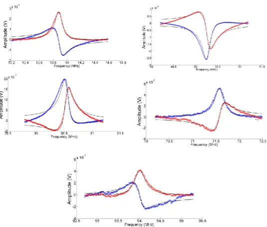
For this device, we detected the frequency shift resulted by the added mass of polymer on first four modes after the functionalization process, which is shown below in Figure 3.9 as a long range sweeps and Figure 3.10 as close-up sweeps of mechanical modes.
38
Figure 3.9: Long range frequency sweep before and after vacuum thermal organic evaporation of PVPh
39
Figure 3.10: Real (red) and imaginary (blue) quadratures of first four modes before (left) and after (right) functionalization process.
40
Table 3.1: Resonance frequencies and quality factors before and after the functionalization process
Mode number
Bare After functionalization with PVPh Resonance Frequency (MHz) Quality Factor Resonance Frequency (MHz) Quality Factor 1st 13.905 105 12.28 101 2nd 30.45 168 27.34 139 3rd 50.17 229 45.89 167 4th 71.49 280 66.72 171
In order to enhance selectivity on NEMS sensors, different polymers can be deposited on the surface as a functional layer to enhance selectivity for the analytes of interest. For this purpose, polymethyl methacrylate (PMMA), is evaporated on blank silicon nitride chips as another functional layer. Progress is promising but further optimization on process parameters are required before actual functionalization of NEMS devices.
Figure 3.11: Images taken with optical microscopy and SEM after vacuum thermal evaporation of PMMA on partially masked silicon nitride chip.
41
4 Gas Sensing Experiment
4.1 Gas Manifold
To test sensor response of functionalized nanomechanical resonator, a vapor generation system is developed. Pure nitrogen is used as a carrier gas and vaporization of organic compounds from liquid to gas phase is provided by gas bubblers. By using a seperate dilution channel and mass flow controller (MFC, Aalborg GFC), vapors can be delivered at particular concentrations ranging from saturated to 0.1% of its saturated concentration at atmospheric pressure and room temperature. Exposure of the analyte to the sensor chamber is initiated by closing normally open to waste 3-way solenoid. After analyte and dilution stream is mixed by the turbulence occuring at the tee connection, a fraction of the gas flow is taken by another MFC and delivered to sensor chamber at a fixed flow rate. Stainless steel and Teflon tubings are used throughout gas manifold, PEEK and fused silica tubings are used throughout the interface between gas manifold and sensor chamber.
The gas standard generation system designed for the generation gas samples consists of two parts. The first part generates analyte of interest at vapor form, where second part is the flow system that allows the generated gases to flow onto the surface of the sensor. The complete system is called as gas manifold in this thesis. After nitrogen gas is introduced to the system as a carrier gas with a fixed flow rate, it passes through a gas bubbler which converts the analyte to gas phase from liquid phase. Gas flow in which analyte has the concentration of its partial vapor pressure, is delivered towards to the sensor chamber with the aid of a normally open-to-waste 3-way solenoid valve. At the configuration where measurement is made, gas is diluted by the nitrogen gas flowing through the dilution channel and directed towards to the sensor chamber.
42
Figure 4.1 represents general architecture of gas manifold. In this figure, there are four streamlines with gas bubblers. With the aid of two way solenoid valves that are placed at the upstream and downstream of each bubbler, one of four analytes can be selected to be sent onto the sensor.
Figure 4.1: Gas manifold and its elements: Mass Flow Controllers, solenoid valves and gas bubblers (from left to right)
Gas bubblers are one of simple methods to generate gas standards. It is based on evaporation of volatile organic compounds (VOC) and concentration of saturated vapor pressure of the volatile organic compounds. Volumetric flow rate at the outlet of the bubbler is higher than the flow rate at the bubbler inlet with respect to the following relation (Eq. 4.1), where VP is vapor pressure of the liquid at its temperature and P is the external pressure:
𝑉̇𝑜𝑢𝑡 = 𝑉̇𝑖𝑛 +
𝑉̇𝑖𝑛 𝑥 𝑉𝑃
43
By tuning the flow rate of the background gas, concentration can be diluted which can be simply calculated as:
𝐶 = 𝑉̇𝑜𝑢𝑡− 𝑉̇𝑖𝑛
𝑉̇𝑜𝑢𝑡+ 𝑉̇𝑑𝑖𝑙 (4.2)
Figure 4.2: Operating principle of a gas bubbler and a picture of gas bubbler that is used in experiments
In the flow system, 99% pure nitrogen (N2) is used as a carrier gas. A commercial hose
(no: 99603N) is assembled to the deliver carrier gas to the gas manifold and flow rate is controlled by Mass Flow Controllers. Nitrogen flow is splitted to two pipelines where carrier gas is used to convert the analyte from liquid to vapor phase and the other one is employed to dilute the concentration of analyte. Background gas is controlled by 0-15 L/min MFC and it directs the flow to the sensor chamber. Flow rate of the gas molecules generated by gas bubbler is controlled by a 0-500 ml/min MFC. At this section, glass is used as a material for gas bubblers to observe and prevent contamination. At the inlets and outlets of gas bubbler, PTFE tubings are attached to connect gas bubbler to the rest of the system, which is mainly composed of stainless steel pipes (6mm outer dimater, 4mm inner diameter). All the connections are checked for gas leakages. Solenoid valves are controlled by using a power supply (12V 3.5A) and switches to address them individually. After passing through the 3-way solenoid valve, analyte vapor reaches the parallel gas line via a T-connection and is directed to the sensor together with the dilution gas. Turbulence formed during the mixing of two
44
different flows of gas at T connection mixes gas and it allows dilution of the sample vapor. The gas manifold is integrated with the rest of the system.
4.2 Sensor Chamber
In order to allow capture of analyte species by active area of the sensor, we designed two different sensor chambers. Initially we used a high volume aluminum sensor chamber when assembling NEMS sensor to the gas manifold, which is shown in Figure 4.3.
Figure 4.3: High volume chamber for gas sensing experiments.
With this sensor chamber, water-vapor is tested on NEMS sensor with bare silicon nitride surface. Water-vapor is sent through the system at 17 parts-per-thousand concentration. Results can be seen from Figure 4.4. In this figure, solenoid that control water-vapor exposure is opened at dashed lines.
However, in such a large chamber (170ml) with respect to the active area of the sensor, time required for analyte to diffuse causes the system to have a long response time. Here, Peclet Number and characteristic number λ determines the diffusion rate and analyte retention [34].
45
We realized that volume of the sensor chamber should be reduced to obtain a faster response from NEMS sensor.
Figure 4.4: Experiments with water-vapor. Water-vapor with the concentration of 17ppth induced (solenoid is opened) between 500-560s, 650-670s, 760-790s and
1100 – 1500s.
As a next step, we reduced the volume of the chamber by assembling a borosilicate glass lid to the carrier (Spectrum Semiconductor Materials) of the NEMS chip, resulting with a volume of 70 µl Glass is drilled with a tungsten carbide drilling tool (PROXXON) to open inlet and outlet ports. After careful alignment, inlet and outlet ports (CapTite) are bonded to the glass lid with a vacuum seal epoxy (LabSmith) and glass lid with the bonded ports is assembled to the chip carrier. Resulting microliter chamber is shown in Figure 4.5.
In order to connect gas manifold to microliter chamber, a reduction scheme in pipeline is designed and employed. Starting from 4mm inner diameter x 6mm outer diameter stainless steel, diameter of pipeline is reduced to 100 µm silica capillary tube by using microfluidic connectors (Fisher Scientific). Gas manifold setup under the fume hood is assembled to the sensor chamber, which is shown in Figure 4.6.
46
Figure 4.5: Microliter chamber
Figure 4.6: Gas manifold under fume hood (a) and reduction scheme from stainless steel pipe to capillary tube (b)
47
In order to analyze the effect of the sealing on the NEMS sensor, resonant responses before and after coating is compared. Without introducing gas flow, slight increase in quality factor is observed (Figure 4.7).
Figure 4.7: Resonant response of NEMS sensor before and after sealing of microfluidic chamber
4.3 Functionalized NEMS as a Detector
After NEMS detectors are assembled to gas manifold, various tests are performed. At first, sensor chamber is purged by nitrogen. At these experiments, we observed that resonance frequency is increased up to 600 kHz (from 28.7 MHz to 29.3 MHz) following a one day purge (Figure 4.8). We interpret this upward drift as a slow desorption of water molecules adsorbed by the surface of the sensor. At the following experiments, 1 day nitrogen purge is used as a protocol in order to desorb the molecules from surface of the sensor.
48
Figure 4.8: Desorption of molecules from surface of NEMS sensor following a nitrogen purge
After desorption of water-vapor molecules from the surface of the sensor, we tested the closed loop response of the NEMS to the physical changes in the system. By using the regulator on the nitrogen tank, we rapidly closed and reopened nitrogen flow. In this way, both the local pressure in sensor chamber and relative humidity is modulated rapidly. NEMS sensor reacted to this modulation on the order of seconds and remained under closed loop.
49
Figure 4.9: NEMS response under nitrogen flow.
To test the response of the NEMS sensors functionalized by poly-vinylphenol (PVPh), we first sent Decanal (C9H19CHO, SigmaAldrich) and 1-iodononane (CH3(CH2)8I,
SigmaAldrich) through the system. Concentrations were 200 parts-per-million for Decanal and 2000 parts-per-million for 1-iodononane. However, we could not observe a distinctive frequency shift for these cancer biomarkers with the sensor functionanized by PVPh. We attribute this result to relatively inert properties of polymer with respect to these analytes of interest.
50
Figure 4.10: Testing 1-iodononane and Decanal on Polyvinylphenol coated NEMS. Even though sensor is exposed to cancer biomarkers in marked area, we could not
observe a distinctive shift on resonance frequency of NEMS sensors.
As a next step, we used Isopropanol Alcohol (IPA) as analyte to observe the response of the poly-vinylphenol coated NEMS. 5ml of IPA is placed inside the gas bubbler and high concentrations of IPA (1 to 9 parts-per-thousand) is generated by gas manifold and sent through the NEMS sensors (Figure 4.11 and Figure 4.12). Since vapor pressure of IPA is relatively high at ambient conditions (P/P0 = 4%) it takes a long
51
the long response time of the system to the slow transportation of the analyte molecules to the sensor chamber and diffusion to the polymer phase rather than response time of the sensor.
52
Figure 4.12: Detection of IPA at various concentrations with PVPh coated NEMS.
By changing the concentrations of IPA during experiments, we also observed a mostly linear relationship between concentration and frequency shift of functionalized NEMS, which can be seen from Figure 4.13.
53
Figure 4.13: Frequency shift of PVPh coated NEMS under different concentrations of IPA
![Figure 1.3: An illustration of adsorption of vapor from gas phase to polymer phase [18]](https://thumb-eu.123doks.com/thumbv2/9libnet/5671240.113562/17.892.262.690.504.764/figure-illustration-adsorption-vapor-gas-phase-polymer-phase.webp)
![Figure 1.4: Identification of chemical warfare agents with polymer coated NEMS [19]](https://thumb-eu.123doks.com/thumbv2/9libnet/5671240.113562/18.892.178.786.490.681/figure-identification-chemical-warfare-agents-polymer-coated-nems.webp)