Performance Characteristics of Digital Current
Detector in DC-DC Converter
Yudai Furukawa, Shusuke Maeda and Fujio Kurokawa
Graduate School of Engineering Nagasaki University
Nagasaki, Japan
Ilhami Colak
Faculty of Engineering and Architecture Gelisim University
Istanbul, Turkey [email protected] Abstract— The purpose of this paper is to present a
performance characteristics of digital current detector in dc-dc converter. The digital peak current mode control dc-dc converter using the voltage-controlled oscillator (VCO) has already proposed. The peak current is detected by using VCO in the proposed method. The gain of amplifier in the current detector affects to the input voltage range of VCO. Also, it affects the transient response. They are discussed by analysing and simulation.
Keywords—digital control, peak current mode control, dc-dc converter, digital current detector
I. INTRODUCTION
In the recent year, the amount of information of server in the data center continues to increase. Therefore, the energy management in data center is very important. The digital control dc-dc converter has attracted attention because it has many advantages such as the energy management, the high performance control and the monitoring task [1]-[7]. The digital control circuit is consisted of the A-D converter and the operation derives. The delay time by the conversion time and the operation time exists in the digital control circuit and it adversely affects the transient response of the system. A digital current mode control method is effective for the improvement of the transient response.
However, when the digital peak current mode control is implemented, a high-speed A-D converter, which is expensive, is required in order to capture the peak current value correctly. The digital controller is also required a high-speed processing enough to turn off signal of the PWM at the timing when the current reaches the peak value. Therefore, implementing the peak current mode control by digital technology is difficult.
The authors have already proposed the digital peak current mode control circuit that does not require the high performance equipment [8, 9]. The proposed circuit converts the current value into the FM pulse by using the inexpensive voltage controlled oscillator (VCO). So that, it is possible to capture the peak current using the digital logic circuit, the programmable delay circuit and VCO. The comparison of
the conventional method in the transient response has already performed. The analysis of controller of proposed circuit is already derived [10].
This paper presents the transient response in changing characteristics of the current detector. The parameter of the amplifier of the current detector contains the derived control gains. We change the current gain and compare the transient of the output voltage respectively by using the simulation.
II. OPERATION PRINCIPLE
Figure 1 shows the circuit configuration of the digital peak current mode control dc-dc converter. The main circuit is composed of the buck type dc-dc converter. In where, Ei is the input voltage, eo is the output voltage, R is the load resistance, iTr is the switching current, Rs is the resistor to detect the switching current, D is the diode, L is the inductance C is the output capacitance iL is the reactor current Tr is the switch and STr is PWM signal. The proposed method uses iTr instead of iL to reduce the loss while Tr is off. eo detected from the main circuit is inputted to the digital control circuit through a preamplifier. The
Fig. 1. Circuit configuration of digital peak current mode control dc-dc converter.
Ei R s R eo
Pre-Amplifier #2
iTr
Digital Control Circuit STr Pre-Amplifier #1 R s iTr C L D Tr iL
voltage RsiTr that is equivalent to the switch current detected by the detection resistor is also inputted to the digital control circuit through a preamplifier. STr is generated by the digital control circuit using these values.
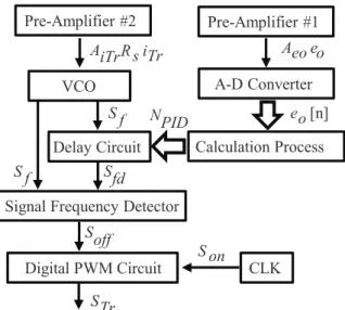
Figure 2 illustrates the circuit configuration of digital control circuit. eo is inputted to A-D converter through the preamplifier. Aeo is the gain of the preamplifier of eo. The amplified voltage Aeoeo is converted to the digital value eo[n] and is inputted to the delay circuit as the calculation results of PID controller NPID. RsiTr is inputted to VCO through the preamplifier of RsiTr. AiTr is the gain of the preamplifier of RsiTr. VCO is an element, which outputs the pulse frequency modulation (PFM) signal. The output signal Sf of VCO and the signal Sfd, that Sf is delayed by a delay
circuit, are sent to the signal frequency detector. In the signal frequency detector, the timing of the turn off signal of the PWM is determined by Sf and Sfd. The signal of the turn on signal Son of the PWM is sent by the CLK. PWM signal STr is determined by this process.
The input-output characteristic of VCO is depicted in Fig. 3. The voltage EVCO is inputted to VCO. EVCOmax and EVCOmin are the maxim value and minimum value, respectively. EVCO is expressed by (1).
( )
Ton EB Tr i s R iTr A VCO E = + (1)where AiTr is the gain of the preamplifier of detected current, iTr(Ton) is the switch current in on period and EB is the bias voltage. VCO outputs the oscillator frequency. The relation of the input voltage and oscillatory frequency is obtained by (2).
( )
{
A R i Ton E}
B A f T B Tr s iTr VCO f + + = = 1 1 (2)where Tf is the one period of Sf, f is the oscillatory frequency,
AVCO is the gain of VCO and B is the intercept of VCO
characteristic. VCO is the characteristic that outputs the oscillatory frequency proportional to the input voltage.
EVCO linearly increases in the proposed method. So, f is
gradually increased and Tf is decreased.
Figure 4 shows the timing chart of digital peak current detector. While STr is on, iTr is linearly increased. Therefore,
Tf is also gradually shortened. Q1 is the signal preset by the
output voltage control loop and is equal to the delay time τ in the signal frequency detector. τ is obtained by (3).
PID N D T ⋅ = τ (3)
where TD is the resolution of delay buffer per one. The turn
Fig. 2. Circuit configuration of digital control circuit.
S f Sfd NPID Pre-Amplifier #2 Pre-Amplifier #1 VCO Delay Circuit Digital PWM Circuit A-D Converter Calculation Process S f STr CLK S on R s iTr AiTr e [n]o Aeo eo
Signal Frequency Detector
Soff 0 f f = A VCO Oscillator Frequ en cy f (MHz) A : gain(MHz/V)VCO AVCO= 3.0
Input Voltage EVCO(V)
min
EVCO EVCOmax
EVCO EVCO
AVCO=1.5
A =1.0VCO
Fig. 3. Input-output characteristic of VCO. Fig. 4. Timing chart of digital peak current detector. f τ T iTr S f S fd Q1 S Tr Ton t
off of STr is determined by the signal frequency detector using Sf and Sfd. The following equation is established when the signal frequency detector outputs the turn off signal.
f
T
=
τ (4)
III. ANALYSIS OF CONTROL GAINS
The control analysis derived by previous research. The peak value of the switch current iTr(Ton) in the main circuit is obtained by (5).
( )
Ton IL( )
0 L L V Ton Tr i = + (5)where VL is the voltage of inductance while the switch is on
Ton is an on time of the main switch and IL(0) is the initial
value of the inductor current. Here, the relational equation (6) of the current detector and the voltage detector is obtained by using (2), (3) and (4).
( )
{
AiTrRsiTr Ton EB}
B VCO A PID N D T + + = ⋅ 1 (6)RsAiTrAVCO in (6) is normalized as follows:
VCO A iTr A s R ICO A = (7)
AICO is the current gain. The equation (8) is derived by
using (5) and (6). The equation (8) represents the equation of
Ton by the output voltage detector and the current detector.
( )
ǻe( )
s H ǻI( )
s s H sH H T s T ǻ L PI o IV DV PV s on − ¿ ¾ ½ ¯ ® + + = (8)HPV is the proportional gain, HIV is the integral gain, HDV
is the differential gain and HPI is the current gain in (8). The control gains in (8) derived by previously research are expressed by the following equations.
2 2 PID N D T ICO A L V PV K s f AD G eo LA PV H = (9) 2 2 2 PID N D T ICO A L V IV K s f AD G eo LA IV H = (10) 2 2 PID N D T ICO A L V DV K AD G eo LA DV H = (11) L s PI V Lf H = (12)
where Aeo is the gain of pre-amplifier, GAD is the gain of A-D converter and fs is the switching frequency. KPV, KIV and
KDV are coefficients of the P control, the I control and the D
control, respectively.
IV. SIMULATION RESULTS
Figure 5 illustrates the input-output characteristics of VCO in the simulation. The range of input voltage is varied by changing the value of AiTr. The ranges I, II and III shown in Fig. 5 are AICO = 5.9 (MHz / A), AICO = 2.9 (MHz / A) and AICO = 2.0 (MHz / A), respectively. The transient responses are compared with each range.
Figures 6, 7 and 8 show the result of the transient response of eo and iL by using the simulation. The step change of the load resistance is from 10 ȍ to 5 ȍ. As the main circuit parameter, Ei is 20 V, eo is 5 V, the switching frequency is 100 kHz, the L is 194 μH, the output capacitance is 990 μF, Rs is 0.05 Ω and R is 5 Ω. KPV, KIV
Fig. 6. Transient responses of eo and iL taking AICO = 5.9 (MHz / A) as a parameter. 5.0 5.4 4.6 5.2 4.8 undershoot: 3.5% t : 1.6mscv e (V) o 1.0 2.0 0 1.5 0.5 0 4.0 8.0 12 16 t (ms) i (A ) L overshoot: 15%
Fig. 5. Input-output characteristic of VCO in simulation.
6.0 10 0 8.0 4.0 1.5 2.0 2.5 3.0 3.5 4.0 4.5 5.0 2.0 I II III Oscillator Frequ en cy f (MHz)
and KDV are equal to 3, 0.05 and 1, respectively. The difference among Figs. 6, 7 and 8 is the value of AICO.
AICO is varied by changing the value of AiTr and the value
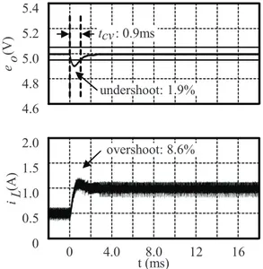
of AVCO is fixed. The value of AICO is equal to 5.9 (MHz / A) in Fig. 6. The convergence time tcv, the undershoot and the overshoot are 1.6 ms, 3.5% and 15%, respectively. In Fig. 7, the value of AICO is equal to 2.9 (MHz / A). tcv, the undershoot and the overshoot are 0.8 ms, 1.6% and 8.6%, respectively. Comparing Fig. 7 with Fig. 6,
the control gains are doubled. So, tcv, the undershoot and the overshoot are improved by 44%, 46% and 43%, respectively. In Fig. 8, the value of AICO is equal to 2.0 (MHz / A). tcv, undershoot and overshoot are 0.6 ms, 1.4% and 6.3%, respectively. Comparing Fig. 8 with Fig. 6, the control gains are tripled. tcv, the undershoot and the overshoot are improved by 63%, 60% and 58%, respectively.
V. CONCLUSION
This paper presents the performance characteristics of the current detector in the digital peak current mode dc-dc converter using VCO. The control gains in the proposed method are also derived. It is discussed that the effect of the value of AICO affects the transient response. A superior transient response is obtained when the value of AICO is 2.0 (MHz / A) compared with the case of AICO = 5.9 (MHz / A).
tcv, the undershoot and the overshoot are improved by 63%,
60% and 58%, respectively, in Fig. 6 and Fig. 8. When smaller value of AICO is set, it is possible to obtain a better transient response. Although the transient response is improved by the smaller value of AICO, the resolution of the current detector is also changed and becomes coarse. Therefore, the proper value should be set to meet both the transient and static characteristics.
REFERENCES
[1] S. Strache, J. H. Mueller, R. Wunderlich and S. Heinen, “Advanced digital current prediction for current ripple reduction in dc-dc converters for photovoltaic applications,” the Proc. the IEEE IECON, pp. 6968-6973, November, 2013.
[2] S. Effler, Z. Lukic and A. Prodic, “Oversampled digital power controller with bumpless transition between sampling frequencies,” in Proc. the IEEE Energy Conversion Congress and Exposition, pp. 3306-3311, September. 2009.
[3] V. Arikatla and A. A. Qahouq, “DC-DC power converter with digital PID controller,” in Proc. the IEEE Applied Power Electronics Conference and Exposition, pp. 327-330, March 2011.
[4] P. Zumel, C. Fernández, M. Sanz, A. Lazaro and A. Barrado, “Simple configurable digital compensator for dc-dc power converters,” in Proc. the IEEE Applied Power Electronics Conference and Exposition, pp. 1208-1214, February. 2009.
[5] S. Saggini, A. Costabeber, and P. Mattavelli “A simple digital autotuning for analog controller in SMPS,” Trans. on IEEE Power Electronics, vol. 25, no. 8, pp. 2170-2178, August 2010.
[6] S. Saggini, A. Costabeber, and P. Mattavelli “A simple digital autotuning for analog controller in SMPS,” Trans. on IEEE Power Electronics, vol. 25, no. 8, pp. 2170-2178, August 2010.
[7] C. H. Tsai, C. H. Yang, J. H. Shiau and B. T. Yeh, “Digitally controlled switching converter with automatic multimode switching,” Trans. on IEEE Power Electronics, vol. 29, no. 4, pp. 1830-1839, April. 2014.
[8] F. Kurokawa and Y. Komichi, “A new peak-current injected digital control circuit for dc-dc converter,” in Proc. the IEEE Power Electronics and Applications, pp. 1-7, August. 2011.
[9] F. Kurokawa, H. Tamenaga, Y. Shibata and Y. Yamabe “Regulation characteristics of fast response digitally peak current controlled dc-dc converter,” in Proc. the IEEE Power Electronics and Drive Systems, pp. 1114-1118, April. 2013.
[10] F. Kurokawa, S. Maeda and Y. Furukawa, “Analysis of digital peak current control dc-dc converter,” in Proc. the IEEE Renewable Energy Research and Application, pp. 737-742, October. 2014. Fig. 7. Transient responses of eo and iL taking
AICO = 2.9 (MHz / A) as a parameter. 5.0 5.4 4.6 5.2 4.8 undershoot: 1.9% t : 0.9mscv 1.0 2.0 0 1.5 0.5 0 4.0 8.0 12 16 t (ms) overshoot: 8.6% e (V) o i (A ) L
Fig. 8. Transient responses of eo and iL taking AICO = 2.0 (MHz / A) as a parameter. 5.0 5.4 4.6 5.2 4.8 undershoot: 1.4% t : 0.6mscv 1.0 2.0 0 1.5 0.5 0 4.0 8.0 12 16 t (ms) overshoot: 6.3% e (V) o i (A ) L