PAPER
Cite this:Nanoscale, 2015, 7, 16110
Received 3rd July 2015, Accepted 2nd September 2015 DOI: 10.1039/c5nr04461h www.rsc.org/nanoscale
Defect related emission
versus intersystem
crossing: blue emitting ZnO/graphene oxide
quantum dots
Sesha Vempati,*
aAsli Celebioglu
a,band Tamer Uyar
a,bIn ref. [Nat. Nanotechnol., 2012, 7, 465–471] interesting optoelectronic properties of ZnO/graphene oxide (GO) composite were presented. Essentially, in the luminescence spectrum indirect optical transitions were identified to be from the epoxy group of GO (GOepoxy) to the valance band (Ev) of ZnO.Viz. 406 nm,
L1: (LUMO+2)GOepoxy → Ev and 436 nm, L2: (LUMO)GOepoxy → Ev. Furthermore, the emission peak at
∼550 nm was attributed to zinc interstitials (Znis) or oxygen vacancies (VOs) and shown to span from
350–650 nm (equivalent to a width of ∼0.8 eV). In this report we accentuate two vital though largely ignored concerns as itemized in the following. (i) By considering the growth mechanism of ZnO in the composite, there is a certain possibility that these two bands (L1 and L2) may originate from intrinsic defects of ZnO such as Znis and extended Znis (ex-Znis). Or L1 and L2 might be intrinsic to GO. (ii) The
550 nm emission involves VOs and consists of two components with a typical width of∼0.3 eV. Here we
present the results of a thorough investigation confirming the presence of Znis, ex-Znis and intrinsic
emission from GO. We also note that during the synthesis the presence of dimethyl formamide signi fi-cantly affected the emission from GO in addition to some chemical modifications. Apart from these, we have discussed other crucial factors which require deeper attention in the context of luminescence from complex systems such as those present.
Introduction
In recent years graphene oxide (GO) has attracted a lot of research attention,1–9 where its potential is evident in its pure form.2,6,10,11 However, the properties can be enhanced/ tuned via combinations2,4,8,9,12–14 especially for optical and optoelectronic applications.3–5,13In any case as a prerequisite, a clear understanding of the emission properties is essential for future developments.2,4,5 For instance, the fluorescence from GO is attributed to the oxygen functional groups (C–O, CvO, and O–CvO) or to the localization of sp2 carbons.2,5
While keeping that in mind, in the case of intercalating struc-tures,2,4the intricacy of the optical properties is of course not abated, where an overlap of the emission bands is present. Nevertheless, we have recently deconvoluted in the case of a GO/polyaniline intercalating compound despite an overlap of emission lines.4It is an undisputed fact that the composites of
GO have great potential2,3,8,9,13,15when combined with other materials such as ZnO,2,3 TiO2,15etc. The emission properties
are strongly dependent on the type of interaction between GO and the other constituent,2,4,14,15e.g. intersystem crossings in TiO2/GO by Bao et al.15and ZnO/GO by Son et al.3Please refer
to ref. 2. for more examples and associated interactions. Among these, the case of ZnO is not only intriguing,3,16but also quite intertwined, especially when the fluorescence from GO superpose with the defect related emission of ZnO.2,16–23 In conjunction with this, we turn our attention to the emission properties of ZnO/GO quantum dots (QDs), precisely to ref. 3. While elucidating the emission properties of GO/ZnO QDs the observed blue emission bands were attributed to transitions L1: (LUMO+2)GOepoxy → Ev and L2: LUMO)GOepoxy → Ev, where
LUMO-lowest unoccupied molecular orbital, GOepoxy-epoxy
groups of GO and Ev is the valance band of ZnO.3 Besides,
green emission is attributed to oxygen vacancies (VOs) or zinc
interstitials (Znis).3
In this report we highlight that the emission wavelengths of Zni → Ev and ex-Zni → Ev overlap with that of L1 and L2,
respectively, where ex-Zni-extended Znis. Despite this, we do
not rule out the earlier discussed transitions,3rather we report
aUNAM-National Nanotechnology Research Centre, Bilkent University, Ankara,
06800, Turkey. E-mail: [email protected]
bInstitute of Materials Science & Nanotechnology, Bilkent University, Ankara, 06800,
Turkey
Published on 08 September 2015. Downloaded by Bilkent University on 28/08/2017 14:22:37.
View Article Online
on evidences of defect related and other emissions which have been largely ignored. Furthermore, the green emission in fact, is attributed to VOs,16–23and consists of two components (bulk
and depletion16,17,19,23), however, not to the presence of Znis.
Since GO can be a p-type material (depending on the level of oxidation),6,10,11in the presence of ZnO it may form a depletion region and influence the emission characteristics as noted here. Furthermore, this report provides a general though vital mapping of crucial factors in analyzing the heterocombinations such as graphene (oxide) and inorganic semiconductors.
Experimental
All the starting materials were received from Sigma and used as received. GO,4,6,7 ZnO QDs,3 and ZnO/GO QDs,3 were syn-thesized as described in the given references. Additionally to reveal the influence of dimethyl formamide (DMF) we have treated GO with it (GODMF) at 95 °C for 5 h which matches the
reaction conditions of ZnO/GO QDs without zinc acetate. These ZnO/GO QDs and GODMF were subjected to repeated
washing with ethanol through centrifugation and finally with deionized water. All the samples were dried at 45 °C overnight under vacuum. Samples were subjected to transmission elec-tron microscopy (TEM, FEI-Tecnai G2 F30) when dispersed in ethanol or deionized water and analyzed from a Cu-grid (without holey carbon coating). TEM images were processed with ImageJ (version 1.42q) software for their fast Fourier transform (FFT) counterparts. X-ray diffraction patterns (XRD) were obtained from a PANalytical X’pert Pro MPD (λCu-Kα =
1.5418 Å). The ionic state of elements at the surface of the samples was investigated by X-ray photoelectron spectroscopy (XPS, Thermoscientific K-alpha, hνAl-Kα = 1486.6 eV) with a
flood-gun charge neutralizer. XPS peak deconvolution was performed with Avantage software. Raman spectroscopy was performed with WITec instruments (Alpha 300S, 532 nm laser). Emission responses were recorded from Horiba Scienti-fic FL-1057 TCSPC at an excitation wavelength of ∼350 nm. Optical emission (Gaussian, standard deviation (SD) ∼2–3 nm), Raman spectra (Lorentzian, SD ∼2 cm−1) and XRD
(Lorentzian, SD ∼0.003°) were deconvoluted with OriginPro 8.5. Apart from the number of peaks, the other parameters were set as free until convergence except the center of two components of the green emission (fixed at 524 (C1) and 577 nm (C2)) based on knowledge from the literature.16,17,19,23 The Raman peak in fluorescence spectra was fixed at∼378 nm for GODMF.
Results and discussion
The ionic interaction between Zn2+ ions and the oxygen-containing functional groups (–O–, –OH and –COOH) of GO is schematized in Fig. 1a–c, after Son et al.3 The differences in the electronegativity/proton donating nature of these func-tional groups enable such an interaction with cations. Based
on this interaction it can be suggested that ZnO QDs growth is initiated on GO where the oxygeneous functional groups are more dense. As a consequence it is expected that the ZnO QDs may not be entirely covered by GO. The effects of the un-covered ZnO are discussed in the emission properties. Contex-tually if the interaction between the adsorbate and substrate is much less than that of the adsorbed molecules themselves, then the influence of substrate on the superstructure can be ignored. In any case, the influence of the substrate on the superstructure will be evident in the structural investigation, e.g. XRD. Furthermore after the growth of the final structure ZnO QDs can host lattice defects, which if radiative, can be identified in photoluminescence (PL). Note that the site specific localized lattice defects will be spatially integrated over the probe beam area (XPS: ∼400 μm2, optical emission: ∼8 mm2, Raman:∼0.13 μm2).
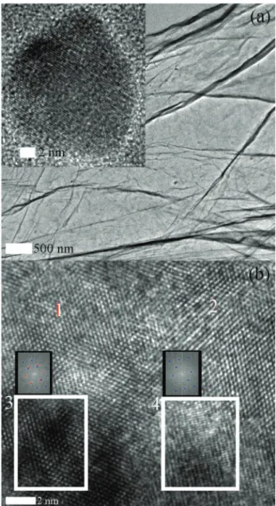
Representative TEM images of GO, ZnO QDs and ZnO/GO QDs are shown along with the FFT in Fig. 2. Probably a single layer of graphene suggests successful exfoliation of graphite while its wrinkles or folds are consistent with earlier reports.4,6,7The ZnO QD is shown as an inset of Fig. 2a. The lattice spacing is found to be ∼2.25 Å, corresponding to the c-axis. A high resolution image from ZnO/GO QDs is shown in Fig. 2b. There are regions annotated with 1 and 2 which clearly show the honeycomb lattice of graphene. Earlier it was antici-pated that ZnO QDs grow on graphene in which context we have selected two regions (3 & 4) for a closer inspection. At first glance, region 3 is darker than 4 presumably due to the differences in the electron transparency either because of the differences in the properties of the material and/or thickness. The FFT counterparts of regions 3 and 4 are shown on top of the selection on Fig. 2b. FFT of region 3 indicated two sets of intensities one of which corresponds to GO (hexagonal shaped, red dots) while the other to ZnO (blue dots). The FFT of region 4 depicted a pattern from the ZnO lattice while that of GO is not seen at an identifiable intensity level. Neverthe-less, the presence of graphene is not denied in region 4, perhaps it may not be in focus due to possible wrinkles and/or folds. This analysis suggests that the ZnO QDs are in fact grown on GO sheets.
XRD-patterns from various samples are shown in Fig. 3 where the corresponding reflections are identified. GO has shown a single reflection depicting an interplanar spacing (dGO) of∼8.379 Å which is consistent with the literature
vis-à-Fig. 1 Interaction between Zn2+ion and (a) epoxy, (b) hydroxyl and (c)
carboxyl groups of GO. Diagram not to scale.
vis dgraphite≈ 3.368 Å.6,7After oxidation the oxygeneous
func-tional groups increase the distance between the graphene sheets which are otherwise stacked under the influence of van der Waal’s force. The pattern from GODMF has sustained the
(002) reflection, however, closer inspection of this peak (Fig. 3b) suggests a shift to a higher Bragg’s angle than that of GO. It appears to be the case that the DMF treatment reduced some of the functional groups bringing the graphene sheets closer (dGODMF = ∼7.968 Å). The consequence of a lowered
degree of oxidation may be reflected in fluorescence2 and
Raman spectroscopy. The pattern from ZnO QDs suggests a polycrystalline wurtzite structure and matches with the litera-ture (Fig. 3a).3,16,17,23Furthermore (100), (002) and (101)
reflec-tions from ZnO containing samples are shown in Fig. 3c. A clear angular shift for ZnO/GO QDs to higher 2θ values results from the developed strain. A closer inspection of the full width at half maximum (fwhm) values of ZnO QDs and ZnO/GO QDs suggests sharper peaks for the former, in other
words higher crystallite size. Furthermore, the peaks from ZnO/GO QDs did not appear to have shoulders at lower 2θ values which rules out the existence of uncovered ZnO QDs within the detection limits of XRD. This is convincing given the fact that Zn2+ ions are hoisted by the oxygeneous func-tional groups and the QD growth takes place on the surface of the GO sheets which is corroborated by TEM investigations. As speculated in the growth model, the ‘substrate (GO) effect’ is reflected in the angular shift of diffraction peaks. In the case of QDs there is not much of a‘bulk’ formed due to their zero dimensions.24The absence of bulk material in fact results in a dramatic effect on its properties as the shift of 2θ corresponds to the whole material (high penetration depth of the probe X-rays25). In the case of the induced stress, additional effects can be expected on optoelectronic properties, in general.26–28 Vacancies or other defects may be formed to relieve the inter-facial strain.29Typically the surface stress (∼1 N m−1) is confined to a distance of 1 nm from the surface.29 Nevertheless, in the course of ZnO/GO QDs synthesis, the possibility of formation of defects such as VOs, Znis etc. are inevitable3,30 which we will
discuss in the context of PL. Furthermore, given the core (ZnO)– shell (GO) structure it is logical to expect an increase in the inter-planar spacing of graphene or stress related effects on ZnO. However, no angular shifts for either (002) of GO or (100), (002) and (101) of ZnO were suggested in ref. 3. While, we have calcu-lated lattice parameters (a and c) of zinc oxide from ZnO QDs and ZnO/GO QDs which are given in the following. aZnO QDs=
3.235, cZnO QDs= 5.186 Å and aZnO/GO QDs= 3.215, cZnO/GO QDs=
5.147 Å. It is apparent that the lattice parameters from ZnO/GO QDs are smaller than that of ZnO QDs. The quantitative changes (%) can be calculated by [a(c)ZnO QDs− a(c)ZnO/GO QDs]/a(c)ZnO QDs
yielding∼0.62 and ∼0.76% for a and c values, respectively.
Fig. 2 TEM images of (a) GO, inset shows a ZnO QD (b) atomic resolved ZnO/GO QD, where FFT image of the boxed region (white) is shown. Red and blue spots correspond to graphene and ZnO lattices, respectively.
Fig. 3 XRD patterns from (a) GO, GODMF, ZnO QDs, ZnO/GO QDs (b)
GO, GODMF(6–15°) and (c) ZnO QDs, ZnO/GO QDs (31–38°) with the
fwhm values and angular shifts annotated.
The atomic percentages (at%) of the constituting elements from the each of the samples are tabulated in Fig. 4a. Core-level XP spectra of O 1s, C 1s and Zn 2p are shown in Fig. 4b–d, while the area ratios of O 1s and C 1s are annotated. We will discuss the C to O ratios later. From Fig. 4a ZnO QDs depict a slightly higher oxygen content than zinc which might be due to the chemisorbed oxygen (OCh) on the surface and
VOs.31,32In the case of ZnO/GO QDs the higher oxygen content
can be from oxygeneous functional groups of GO. However, we expect some contribution from OCh. Carbon from ZnO QDs
might have arose from atmospheric contamination, or glue from the copper tape that we used to load the samples into the analysis chamber, in addition to a fraction of residual starting materials. The same is true for ZnO/GO QDs, however additional contributions to the carbon comes from graphene. The energetic location of O 1s from ZnO (OZnO) is consistent
with the literature (∼530.4 eV, Fig. 4b).17,31,33O
Chappeared at
532.2 eV indicating incorporation of–OH, –CO, adsorbed H2O
and/or O2or O−and O−2ions17,33–35essentially occupying the
VOs which play a critical role in the emission properties and
related applications.16,17,31,32
C 1s spectra from GO, GODMF, ZnO/GO QDs suggested three
oxygeneous functional groups (C–O, CvO and O–CvO) with varying fractions apart from CvC (Fig. 4c).33GO has depicted
a ratio of C : O::0.82 : 1.44. During the oxidation process oxy-geneous functional groups are implanted on the basal plane and edges of the graphene sheets.7 This covalent functionali-zation increases the interplanar distance as evidenced in the XRD. Analysis on GO and GODMF suggest that total O at
% decreased apart from some N incorporation presumably due to DMF treatment (GODMFC : O::1.38 : 1). It is also noted
that a fraction of conversion of CvO to C–O may be originated from the protonation of carbonyls by–CH3groups of DMF. On
the other hand, for the increase of O–CvO, the presence of –OH ions was attributed. It is convincing as we did not use anhydrous solvent in addition to the hydrophilic nature of GO. Further ZnO/GO QDs have shown C : O::1.93 : 1 which is higher than that of GODMF. In the former case, due to the presence of
Zn2+ions some of the functional groups are shielded in con-trast to GODMF. This shielding hindered the access to DMF
leaving the functional groups unreduced. We will see that in the context of Raman with a slightly increased interplanar spacing of GO due to the presence of ZnO QDs. The changes in the density of oxygeneous functional groups are consistent with the observation in XRD. In ref. 3 the analysis of O 1s core-level spectrum suggested fractional contributions are about 22% (C–O); 54% (O–CvO) and 22% (CvO) (Fig. S3–2, ESI of ref. 3). Due to the presence of DMF during the synthesis, CvO will be converted into C–O, apart from an increase in the O– CvO group. The presence of O–CvO groups in such high con-centrations requires a full consideration in the context of opto-electronic properties which is not the case in ref. 3. On the other hand the presence of CvO functional groups (Fig. S3–2(b), ESI of ref. 3) is not discussed3 in the context of interaction with Zn2+in addition to its electron-trapping capability under an excited state.4,36 These groups do interact with Zn2+ however, depending on the strength of the acidic nature.6The integral effect of all the existing oxygeneous functional groups form the QDs during the reaction.
Moving onto Fig. 4d, Zn 2p from ZnO QDs and ZnO/GO QDs were compared with literature.17,32For both the cases the doublet peak positions (Zn 2p3/2 and Zn 2p1/2 at
∼1021.5 and ∼1044.5 eV, respectively) and fwhm values match with the literature.17,31–33 Apart from the Zn 2p doublet two additional peaks (*2p3/2 and *2p1/2 shaded in green) are
observed at higher binding energies for both the samples. These peaks are attributed to the presence of Znis,17,32,33
however, such a deconvolution of ionic state should be corro-borated appropriately. In line with this we have co-plotted the normalized spectra from QDsZnO# and ZnO## where the
former consists of significant density of Znis while the latter is
a well developed grainy coating (data taken from the # ref. 17 and ## ref. 32). Znis are seen to occur in the presence of an
inhomogeneous distribution of functional groups on the surface of the substrate17apart from Zn rich environments.20 Interestingly, although at present the substrate is not the same as that of ref. 17 the interaction between the functional groups and Zn2+appears to play a crucial role. Please consult ref. 17 for further details on synthesis and structure. The high energy tails of the Zn 2p3/2 and Zn 2p1/2 need to be inspected for
Fig. 4 (a) Atomic %, (b) O 1s from ZnO QDs, (c) C 1s from GO, GODMF,
ZnO/GO QDs and (d) Zn2p from ZnO QDs, ZnO/GO QDs, normalized plot compares with ZnO. Data taken from the # ref. 17 and ## ref. 32.N
normalized intensity scale.
shoulder like structure (boxed region on Fig. 4d, bottom). In the case of QDsZnO# the shoulder at higher energy is quite
clear. It is notable that the intensity of the shoulder decreases ZnO/GO QDs, ZnO QDs and ZnO## in that order. As we can see in the case of well developed and virtually defect free (Zn-related) surface there is no shoulder. This analysis essentially suggests the presence of Znis in ZnO/GO QDs and ZnO QDs of
varying density which will be revealed through specific energy lines in the PL.
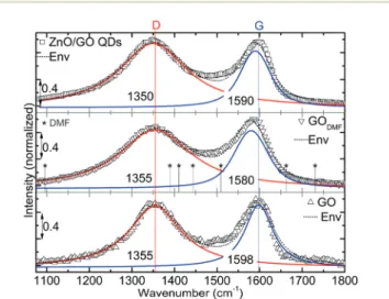
The Raman spectrum of GO is characterized by two main components, D and G bands. D-band: edges, defects or the breakdown of translational symmetry. G-band: first order scat-tering of E2g phonon of sp2carbon atoms.37Raman response
from GO, GODMFand ZnO/GO QDs are shown Fig. 5. Spectrum
from GO has shown two signature peaks at ∼1355 and ∼1598 cm−1 corresponding to D and G bands, respectively.
Interestingly the peak at∼1355 cm−1did not show any signifi-cant spectral shift for the two modifications while the latter is shifted to ∼1580 and ∼1590 cm−1 upon DMF treatment and ZnO QDs growth process, respectively. It might be the case that the distance between the graphene sheets is decreased37 (lowered density of oxygeneous functional groups) upon DMF treatment. However, due to the ZnO QDs and/or sustained degree of oxidation (interacting Zn2+) the distance between the sheets is increased again and the G-band is recovered to an extent. However, this is not seen explicitly in the XRD due to relatively lower signal to noise ratio. It is not denied that the DMF treatment might increase the already established defects such as changing bond lengths, angle and disorder at the atomic scale which eventually softens the phonon modes.37If this is the case then the G-band may not recover to 1590 cm−1 for ZnO/GO QDs. Hence the softening of phonons is attributed to the decreased distance between the sheets rather than any other attribution. Note that the shift is not due to adsorbed DMF as no overlap of the peaks (‘★’ on Fig. 5) is seen within the detection limits. From Raman studies, it is also clear that
the graphene in ZnO/GO QDs is not identical to that of GODMF
in all aspects as expected due to the growth of ZnO QDs. Such changes in the degree of oxidation can be seen in the context of fluorescence properties.2,5Son et al.3noticed splitting of the G-band for ZnO/GO QDs (G− and G+ at 1566.6 and 1592.7 cm−1respectively) and attributed it to uniaxial strain on graphene (monolayer) under a first order approximation.38In contrast to ref. 3 uniaxially bent graphene layer38has shown G−and G+at∼1563 and ∼1576 cm−1(approximated from the plot), i.e. the G band splits and shifts to lower frequencies whereas G+ has shown a significant blue shift of ∼17 cm−1. This shift cannot be attributed to the‘assumption’ of uniaxial strain3however biaxial strain is certainly closer to the ZnO/GO QDs case due to the spherical structure of QD. Nevertheless, in the case of biaxial strain no splitting is observed39–41 apart from the red-shifted G-band.39 Although biaxial strain better represents the core–shell configuration in ref. 3 the blue shift of G+might have arisen mainly due to ZnO. Notwithstanding, the presence of strain is not excluded in the current scenario. Contextually note that in the case of electron doping the G band blue shifts.42On the other hand, the presence of 3 at% of N might cause significant change in the electron density of GO thus the position of G band. Nevertheless, a deeper under-standing of the influence of ZnO QDs under strain on the Raman modes of graphene is warranted.
We have analyzed the emission properties of GO, GODMF,
ZnO QDs and ZnO/GO QDs and plotted them in Fig. 6a–d respectively. L1 and L2 on part (b) indicate the spectral overlap of the emission peaks and hence are not to be attributed to Znis and ex-Znis. In ref. 3 the earlier mentioned lines, L1 and
L2 are attributed to GOepoxy and Ev transitions (intersystem
crossings3,15), see Fig. 6e (Ec-conduction band and EF-Fermi
level). However, in XPS the presence of Znis and possible
for-mation of ex-Znis is evidenced3,30while their emission is
sche-matized in Fig. 6f. In what follows is a discussion of each of the samples in relation to the present attribution and the origin of the green emission. In general, the intrinsic lattice defects and surface states are predominant in QDs.24In the case of ZnO it is known that visible emission occurs from the surface18,21,22in which case, the extremely high surface area to volume ratio of QDs plays a critical role. To begin with, the fluorescence from GO is under intense discussion.2,5The peak annotated with R is due to Raman scattering which occurred at∼378 nm (∼350 nm illumination) for both GO and GODMF.
An overview of recent literature on the emission from GO and reduced-GO is given in ref. 2. Emission from GO is excitation dependent (see ref. 86–88 in ref. 2) and attributed to the various possible transitions from the minimum of the conduc-tion band to localized states in the valance band. Basically the fluorescence from GO is explained based on two arguments. 1. The presence of oxygeneous functional groups on the basal plane. In this case the emission occurs from zigzag sites of GO where their ground state is in a triplet state similar to carbene, 2. quantum confinement of sp2 domains (π-electrons) and e/h recombination therein. In this case, the local band gap depends on the size of the cluster. For GODMF
Fig. 5 Raman spectra from GO, GODMFand ZnO/GO QDs with peak
deconvolution. Modes from pure DMF are denoted with★. The spectral locations were annotated in cm−1.
the reaction with DMF incorporated nitrogen (XPS and Raman) which can influence the emission characteristics via doping the GO. Going into specifics, for GO (Fig. 6a) two peaks are noted in the blue region at ∼416 and ∼452 nm (apart from two more components) which were slightly blue shifted to∼409 and ∼434 nm respectively, for the GODMFcase
(Fig. 6b).2 Based on the literature and the available
expla-nation2we believe that these two blue emissions may be due to confinement of sp2 domains. The blue shift of the blue emission may be due to increased confinement after DMF treatment. After DMF treatment the other two peaks at 520 and 597 nm have almost distinguished. This can be due to the overall decrease in the degree of oxidation, d value (dGO > dGODMF) and conversion of some functional groups.
2,5
Hence these higher wavelength peaks may be attributed to the oxygeneous functional groups. Interestingly the blue emission peaks from GODMF (∼409 and ∼434 nm) spectrally overlap with
that of L1: (LUMO+2)GOepoxy→ Evat 406 nm and L2: (LUMO)GOepoxy
→ Evat 436 nm from ref. 3. We wish to point out that the
emis-sion bands may be due to the GODMFjuxtaposing with the
pro-posed intersystem crossing. This spectral overlap is crucial to address and rule-out the possibility of emission from GODMF.
The PL/optical emission spectra from ZnO QDs and ZnO/GO QDs are shown in Fig. 6c and d, respectively. The band gap of each sample is calculated as the sum of exciton emission and its binding energy (60 meV) yielding 3.31 eV and 3.36 eV for ZnO QDs and ZnO/GO QDs, respectively (Fig. 6f ). The slight increase in the band gap can be attributed to the quantum confinement effect, in line with the earlier discussed growth mechanism. The 2D growth of ZnO on the surface of GO enhanced the confinement from pristine QDs. The green-emis-sion from ZnO is attributed to VOs consisting of two
com-ponents. Specifically, C1: 524 nm (2.37 eV): V*
O! Ev, and C2:
577 nm (2.15 eV) Ec → V++O, which take place in bulk and
depletion regions, respectively (inset of Fig. 6c).16,18,19,21–23,43 V+Ostates either capture an electron (e) or hole (h) from Ecor Ev
respectively, i.e. VþOþ e ! V*Oand V+O+ h→ V++O. Furthermore,
the area ratios of C1 to C2 across the two ZnO containing samples are considered which reflect the emission from the corresponding regions. The ratios are (C1 : C2)ZnO QDs::1 : 0.93;
(C1 : C2)ZnO/GO QDs::1 : 1.87. Explicitly in the ZnO/GO QDs
sample there is almost a two-fold variation in the area of
C2.16,19The enhanced C2 emission is convincing because of
the fact that the GO6,10,11 and ZnO16,19 are p- (depending on the degree of oxidation) and intrinsic n-type materials, respect-ively. The volume of the depletion region is increased due to the presence of GO which enhances C2 as we observed here. Note that in the ZnO QDs case the occupancies of VOs form
the depletion region. To further comment on this, the observed changes in the relative emissions of C1 and C2 may not be an interfacial quenching, which requires a transfer of photoexcited electrons from Ecof ZnO to EFof graphene.44In
this case the whole emission is expected to decrease. However, we don’t completely rule out such a possibility if the GO is sufficiently metallic within the interface.
In the blue region of ZnO QDs two peaks are seen, 405 nm (L1) and (435) L2 while the latter depicted relatively low inten-sity. Zn 2p core-level spectrum evidenced the presence of Znis
in smaller density from ZnO QDs which is reflected in the PL. The above two lines are attributed to Znis and ex-Znis,
respect-ively (L1: Zni→ Evand L2: ex-Zni→ Ev)20and consistent with
the literature.17,20,23 Znis are about 0.22 eV below the
Ec,45while ex-Znis are∼0.5 eV below Ec.20Under suitable
illu-Fig. 6 Fluorescence from (a) GO, (b) GODMF, PL/optical emission from
(c) ZnO QDs, (d) ZnO/GO QDs, (e) schematic of the two emission lines redrawn after Sonet al.3and (f ) ZnO/GO QDs with defect levels Zn
iand
ex-Znistates, insert of (c) depicts the schematic of the green emission
from ZnO. Area ratio is indicated with reference to that of 524 nm the (C1) peak in the respective sample.Ec,Evare conduction and valance
bands, respectively, while ecptrand hcptrare electron and hole capture
processes, respectively, andEFis the Fermi level. L1 and L2 on part (b)
only indicate the spectral overlap of the emission peaks and hence should not be attributed to Znis and ex-Znis.
mination, electrons are excited to the Ec, which are then
non-radiatively transitioned into Znis or ex-Zni. Also electron
trans-fer can take place from Znis to ex-Zniand subsequently to Ev.
These localized electrons recombine with free holes in the Ev leading to violet or blue emission.20 The presence of GO
prior to the formation of ZnO QDs has a significant influence on its growth, where the Zn2+ ions are anchored to the oxy-geneous functional groups of GO. Also, during the growth GO-sheets enclose the QD either partially or completely (Fig. 2 and Fig. 2 of ref. 3). Although the GO sheets are flexible, XRD results suggest spatial or physical restriction that is imposed on interacting-Zn2+ions which may cause lattice defects such as Znis on the surface.17,20Zn 2p core-level spectra suggest a
slightly higher density of Znis in ZnO/GO QDs than that of
ZnO QDs, which is clearly reflected in the emission. These Znis form ex-Zni states20as we can see the prominent di
ffer-ence in L2 across the two samples. For ZnO QDs, L1 due to Znis should occur at 3.09 eV which is at 3.05 eV with reference
to the band gap (abbreviated as‘L1-ZnO QDs|Znis: 3.09/3.05
eV’). Similarly L2-ZnO QDs|ex-Znis: 2.8/2.86 eV, L1-ZnO/GO
QDs|Znis: 3.14/3.03 eV and L2-ZnO QDs|ex-Znis: 2.85/2.85 eV.
A small disagreement between the emitted and expected lines is due to the differences in the band gap, the error involved in the deconvolution procedure. Especially for ZnO/GO QDs it can be a combination with the fluorescence from GO. The presence of CvO functional groups may decrease the quantum efficiency of the ZnO/GO QDs by trapping the elec-trons under an excited state.4,36The consequences of trapping will be explicit in the context of optoelectronic properties as noted earlier.4 However, the efficiency of trapping of photo-excited electrons is determined by its recombination dynamics and physical accessibility, i.e. the functional group must be fast enough to trap the electron before the recombination. It is also notable that the recombination dynamics are influenced by electron and hole mobilities against the intrinsic electric field due to the depletion layer. Given this the complete quenching of emission from ZnO due to CvO groups can be an ideal scenario. Furthermore, since emission is seen from ZnO/GO QDs, it is believed that the density of CvO was not high enough to quench the emission completely, where the DMF treatment has converted the CvO groups in to C–O groups. Earlier it was mentioned that the ZnO QDs are not fully covered by GO. However, the fraction of which can be very low and it would not undermine the discussion. The uncovered ZnO would not suppress the emission from ZnO/GO QDs rather we observe an integral effect from both uncovered ZnO and ZnO/GO QDs depending on their relative fractions. In the mixed case the peak area corresponding to the intrinsic defects cannot be simply attributed to individual constituents (when the exact fraction is unknown). Nevertheless, the defect emission wouldn’t change its spectral position and should be evident in the PL. The existence of uncovered ZnO QDs in large fractions is unlikely, for instance the XRD of ZnO/ GO QDs did not depict any peaks with shoulders, which shows the contribution from uncovered ZnO QDs. On the other hand, XRD evidenced significant stress on the ZnO lattice in ZnO/GO
QDs, viz. the quantitative changes were ∼0.62 and ∼0.76% for a and c values, respectively. Xu et al.26suggested a piezotro-nic effect on the PL of ZnO nanowires (NWs) where excitonic emission red-shifts with increasing stress. Essentially the piezoelectric field (±φ) redistributes the photoexcited carriers along with a modified band structure of a bent ZnO NW causing a red-shift. The following parameters determine the presence of the piezotronic effect. (a) |φ| critically depends on the doping density (ND) while the latter can partially or totally
screen theφ.28(b) For W≪ dNWthe red-shift is independent of
the dNWwhere W– width of the depletion layer and dNW–
dia-meter of the nanowire. When W≈ dNWthe red-shift is dependent
on the dNW, which decreases with decreasing dNW26 (c) single
crystals depicted piezotronic26 and piezoelectric response27,28 (when bent along the c-axis) and highly c-axis oriented thin films46exhibited a piezoelectric response. In the present case we did not observe any piezotronic effect in the ZnO/GO QDs despite the strain due to the following reasons corresponding to the above factors. (a′) For ZnO, NDis determined by point defects
such as Znis and VOs.47ZnO QDs consists of intrinsic defects
(Znis and VOs) as explicitly evidenced in the PL (Fig. 6c). The
same is true for ZnO/GO QDs (Fig. 6d) where the defects are more pronounced and hence the relatively higher NDscreening
the φ. (b′) For QDs, W is most probably as thick as the dia-meter. Moreover, W would be relatively higher for the ZnO/GO QDs case due to the p-natured GO (seen from the area ratios of green emission). Since W≈ dNWany shift is governed by the
size of the QDs. From Fig. 5c of ref. 26, as the diameter of the NW decreases the red-shift of the free exciton emission decreases, essentially approaching W≈ dNW. (c′) ZnO QDs and
ZnO/GO QDs are polycrystalline without any preferential orien-tation. Piezotronic response is realized when a compressive strain is applied along the c-axis of NW26,28while a is allowed to modulate most probably increasing its value. Significantly, here c and a were subjected to compressive strain. It may be the case that the developedφ along one axis is compensated by the other axis. Furthermore, theφ may be compensated by GO, where there is a net supply of electrons from GO despite it being a p-type material.6,10,11
Conclusions
The ionic interaction between Zn2+ ions and the oxygeneous functional groups influence the growth of ZnO QDs, where the lattice of the latter is slightly compressed. Due to the previously mentioned interaction XPS evidenced Znis where their density
in ZnO/GO QDs is higher than that of the pristine counterpart. Analyses of Raman spectra suggested a deeper investigation was needed to understand the influence of ZnO on GO. We do acknowledge the fact that the analysis of the optical emission from complex systems is not a simple arithmetic sum of two or more components, but involves various combinatory factors. Nevertheless, we provide direct conclusions with spectroscopic evidence on two vital issues regarding the mechan-ism of luminescence from the ZnO/GO composite. (i) L1 and
L2 have two alternative possibilities, viz. Zni→ Evand ex-Zni→
Evrespectively and (ii) these two emissions might be from GO.
The interaction between GO and Zn2+is the basis for the exist-ence of Znis as evidenced in the XPS and subsequently in PL.
Also the presence of Znis can perhaps explain the emission
from the light emitting diode structure in ref. 3. Under biased conditions the charge carriers may be injected from GO into the Zni or ex-Znistates which eventually recombine with free
holes in the Evemitting light of matching wavelength.
Lumine-scence centered at 550 nm is attributed to VOs with two
com-ponents and a width of about 0.3 eV each in contrast to 0.8 eV shown in ref. 3. In the ZnO/GO QDs the emission from the depletion region is enhanced twice due to the presence of GO. The absence of the piezotronic effect in ZnO/GO QDs despite a significant strain is attributed to the increased ND, W ≈
diameter of the QDs, compressive strain along c and a axes and to the presence of GO.
Acknowledgements
S. V. thanks The Scientific & Technological Research Council of Turkey (TUBITAK) (TUBITAK-BIDEB 2221-Fellowships for Visiting Scientists and Scientists on Sabbatical) for the post-doctoral fellowship. A. C. thanks to TUBITAK (Project no. 113Y348) for the postdoctoral fellowship. T. U. acknowledges The Turkish Academy of Sciences– Outstanding Young Scien-tists Award Program (TUBA-GEBIP).
Notes and references
1 A. M. Dimiev and J. M. Tour, ACS Nano, 2014, 8, 3060– 3068.
2 S. Vempati and T. Uyar, Phys. Chem. Chem. Phys., 2014,16, 21183–21203.
3 D. I. Son, B. W. Kwon, D. H. Park, W. S. Seo, Y. Yi, B. Angadi, C. L. Lee and W. K. Choi, Nat. Nanotechnol., 2012,7, 465–471.
4 S. Vempati, S. Ozcan and T. Uyar, Appl. Phys. Lett., 2015, 106, 051106.
5 K. P. Loh, Q. L. Bao, G. Eda and M. Chhowalla, Nat. Chem., 2010,2, 1015–1024.
6 S. Vempati, A. Celebioglu and T. Uyar, J. Mater. Chem. C, 2014,2, 8585–8592.
7 D. C. Marcano, D. V. Kosynkin, J. M. Berlin, A. Sinitskii, Z. Sun, A. Slesarev, L. B. Alemany, W. Lu and J. M. Tour, ACS Nano, 2010,4, 4806–4814.
8 B. Yao, C. Li, J. Ma and G. Shi, Phys. Chem. Chem. Phys., 2015,17, 19538.
9 P. Shao, J. Tian, B. Liu, W. Shi, S. Gao, Y. Song, M. Ling and F. Cui, Nanoscale, 2015,7, 14254.
10 R. J. W. E. Lahaye, H. K. Jeong, C. Y. Park and Y. H. Lee, Phys. Rev. B: Condens. Matter Mater. Phys., 2009, 79, 125435.
11 M. Jin, H.-K. Jeong, W. J. Yu, D. J. Bae, B. R. Kang and Y. H. Lee, J. Phys. D: Appl. Phys., 2009,42, 135109.
12 S. Mondal, U. Rana and S. Malik, Chem. Commun., 2015, 51, 12365.
13 Q. Luo, Y. Zhang, C. Liu, J. Li, N. Wang and H. Lin, J. Mater. Chem. A, 2015,3, 15996.
14 Y. Wang, Y. Li, W. Qi and Y. Song, Chem. Commun., 2015, 51, 11022–11025.
15 S. S. Bao, Z. Hua, X. Y. Wang, Y. Zhou, C. F. Zhang, W. G. Tu, Z. G. Zou and M. Xiao, Opt. Express, 2012,20, 28801–28807.
16 S. Vempati, S. Chirakkara, J. Mitra, P. Dawson, K. K. Nanda and S. B. Krupanidhi, Appl. Phys. Lett., 2012,100, 162104. 17 F. Kayaci, S. Vempati, I. Donmez, N. Biyikli and T. Uyar,
Nanoscale, 2014,6, 10224–10234.
18 K. Vanheusden, C. H. Seager, W. L. Warren, D. R. Tallant and J. A. Voigt, Appl. Phys. Lett., 1996,68, 403.
19 J. D. Ye, S. L. Gu, F. Qin, S. M. Zhu, S. M. Liu, X. Zhou, W. Liu, L. Q. Hu, R. Zhang, Y. Shi and Y. D. Zheng, Appl. Phys. A: Mater. Sci. Process., 2005,81, 759.
20 H. Zeng, G. Duan, Y. Li, S. Yang, X. Xu and W. Cai, Adv. Funct. Mater., 2010,20, 516–572.
21 A. v. Dijken, E. A. Meulenkamp, D. Vanmaekelbergh and A. Meijerink, J. Phys. Chem. B, 2000,104, 1715.
22 K. Vanheusden, W. L. Warren, C. H. Seager, D. R. Tallant, J. A. Voigt and B. E. Gnade, J. Appl. Phys., 1996,79, 7983. 23 S. Vempati, J. Mitra and P. Dawson, Nanoscale Res. Lett.,
2012,7, 470.
24 S. Vempati, Y. Ertas and T. Uyar, J. Phys. Chem. C, 2013, 117, 21609–21618.
25 X-ray penetration depth (1/e of intensity,δ) = 1/(ξρ), where ρ-density (g cm−3) and ξ-mass attenuation coefficient
(cm2g−1).ξ was taken from [http://physics.nist.gov/PhysRef-Data/XrayMassCoef/tab3.html].ξZn= 58.75,ξO= 11.63,ξZnO
=ξZn+ξO,ρZnO= 5.61;ξgraphite= 4.57,ρgraphite= 2.27;
yield-ingδZnO=∼25 μm and δgraphite=∼960 μm.
26 S. Xu, W. Guo, S. Du, M. M. T. Loy and N. Wang, Nano Lett., 2012,12, 5802–5807.
27 B. Wei, K. Zheng, Y. Ji, Y. Zhang, Z. Zhang and X. Han, Nano Lett., 2012,12, 4595–4599.
28 Z. L. Wang, J. Phys. Chem. Lett., 2010,1, 1388–1393. 29 H. Luth, Solid Surfaces, Interfaces and Thin Films, Springer,
5th edn, 2010, ISBN 13591-0, e-ISBN 978-3-642-13592-7, DOI: 10.1007/978-3-642-13592-7.
30 S. Niyogi, E. Bekyarova, M. E. Itkis, J. L. McWilliams, M. A. Hamon and R. C. Haddon, J. Am. Chem. Soc., 2006, 128, 7720–7721.
31 F. Kayaci, S. Vempati, C. O. Akgun, I. Donmez, N. Biyikli and T. Uyar, Appl. Catal., B, 2015,176–177, 646–653. 32 F. Kayaci, S. Vempati, C. O. Akgun, I. Donmez, N. Biyikli
and T. Uyar, Nanoscale, 2014,6, 5735–5745.
33 A. V. Naumkin, A. K. Vass, S. W. Gaarenstroom and C. J. Powell, 2012, NIST Standard Reference Database 20, Version 4.1.
34 M. Chen, X. Wang, Y. Yu, Z. Pei, X. Bai, C. Sun, R. Huang and L. Wen, Appl. Surf. Sci., 2000,158, 134–140.
35 A. Stănoiu, C. E. Simion and S. Somăcescu, Sens. Actuators, B, 2013,186, 687–694.
36 H. Chang, Z. Sun, Q. Yuan, F. Ding, X. Tao, F. Yan and Z. Zheng, Adv. Mater., 2010,22, 4872.
37 A. C. Ferrari, Solid State Commun., 2007,143, 47–57. 38 T. M. G. Mohiuddin, A. Lombardo, R. R. Nair, A. Bonetti,
G. Savini, R. Jalil, N. Bonini, D. M. Basko, C. Galiotis, N. Marzari, K. S. Novoselov, A. K. Geim and A. C. Ferrari, Phys. Rev. B: Condens. Matter Mater. Phys., 2009,79, 205433. 39 J. Zabel, R. R. Nair, A. Ott, T. Georgiou, A. K. Geim, K. S. Novoselov and C. Casiraghi, Nano Lett., 2012,12, 617– 621.
40 F. Ding, H. Ji, Y. Chen, A. Herklotz, K. Dorr, Y. Mei, A. Rastelli and O. G. Schmidt, Nano Lett., 2010,10, 3453.
41 C. Metzger, S. Remi, M. Liu, S. V. Kusminskiy, A. H. N. Castro, A. K. Swan and B. B. Goldberg, Nano Lett., 2010,10, 6. 42 S. Pisana, M. Lazzeri, C. Casiraghi, K. S. Novoselov,
A. K. Geim, A. C. Ferrari and F. Mauri, Nat. Mater., 2007,6, 198.
43 M. Ghosh and A. K. Raychaudhuri, Nanotechnology, 2008, 19, 445704.
44 EFequilibration takes place when the materials are brought
into contact.
45 C. H. Ahn, Y. Y. Kim, D. C. Kim, S. K. Mohanta and H. K. Cho, J. Appl. Phys., 2009,105, 013502.
46 I. K. Bdikin, J. Gracio, R. Ayouchi, R. Schwarz and A. L. Kholkin, Nanotechnology, 2010,21, 235703.
47 Y. Gao and Z. L. Wang, Nano Lett., 2009,9, 1103–1110.