Semiconductor Science and Technology
PAPER
Determination of the band gap of indium-rich InGaN by means of
photoacoustic spectroscopy
To cite this article: Robert Oliva et al 2018 Semicond. Sci. Technol. 33 035007
View the article online for updates and enhancements.
Determination of the band gap of indium-rich
InGaN by means of photoacoustic
spectroscopy
Robert Oliva
1,6, Szymon J Zelewski
1,6,
Łukasz Janicki
1,
Katarzyna R Gwó
źdź
2, Jaros
ław Serafińczuk
3, Mariusz Rudzi
ński
4,
Ekmel
Özbay
5and Robert Kudrawiec
11
Department of Experimental Physics, Faculty of Fundamental Problems of Technology, Wroclaw University of Science and Technology, Wybrzeże Wyspiańskiego 27, 50-370 Wrocław, Poland
2
Department of Quantum Technologies, Faculty of Fundamental Problems of Technology, Wroclaw University of Science and Technology, Wybrzeze Wyspianskiego 27, 50-370 Wroclaw, Poland
3
Faculty of Microsystem Electronics and Photonics, Wroclaw University of Science and Technology, Janiszewskiego 11/17, 50-372 Wrocław, Poland
4Institute of Electronic Materials Technology, Wólczyńska 133, 01-919 Warsaw, Poland 5
Nanotechnology Research Center, Bilkent University, 06800 Bilkent, Turkey E-mail:[email protected]
Received 4 December 2017, revised 15 January 2018 Accepted for publication 19 January 2018
Published 5 February 2018 Abstract
Photoacoustic(PA) measurements have been performed on a series of InxGa1−xN thinfilms grown with x>50%. In order to illustrate the usefulness of this technique, these measurements have been compared with the results obtained by the following conventional techniques: photoluminescence, transmittance and contactless electroreflectance. Amongst all these techniques, only PA spectroscopy exhibited signal without the undesired Fabry–Perot
interferences arising from the thinfilm and buffer layer. By accurately assessing the strain state and composition of our samples, we were able to study the compositional dependence of the band gap of our epilayers. Our results show that a bowing parameter of 1.43 eV successfully describes the compositional dependence of the band gap of InGaN.
Keywords: InGaN, bowing parameter, contactless electroreflectance, photoacoustic spectroscopy, photothermal spectroscopy
(Some figures may appear in colour only in the online journal) 1. Introduction
Since the correct determination of the band gap of InN (0.65 eV) a great deal of research has been paid to the InGaN alloy system since its band gap can be tuned to cover the entire visible spectral range, from the ultraviolet(3.4 eV for GaN) down to near-infrared wavelengths [1, 2]. Such a unique property could be exploited to design novel devices including high-efficiency multijunction solar cells. Most importantly, the demonstration of InGaN-based inexpensive
high-brightness blue LEDs boosted the interest in this alloy system[3,4].
Despite the large interest of InGaN for optoelectronic devices, the compositional dependence of the band gap is not precisely established. In particular, works reporting the band gap of In-rich InGaN do not take into account residual strain effects[5] or the Burstein–Moss (BM) shift which can lead to an overestimation of the band gap as high as 200 meV[6,7]. Aside from the effects of electron concentration and strain on the optical band gap, compositionalfluctuations also make the determination of the band gap of InGaN difficult. Composi-tional inhomogeneities result in an increased Stokes shift, which might yield to energy differences between PL and Semicond. Sci. Technol. 33(2018) 035007 (6pp) https://doi.org/10.1088/1361-6641/aaa908
6
absorption as high as 500 meV for InGaN [5]. Therefore, owing to the many intrinsic difficulties of the InGaN band gap characterization the use of alternative techniques is desirable. Photoacoustic spectroscopy (PA) has demonstrated to be a reliable technique that can be used to determine the band gap of semiconductor alloys [8–10], including InGaN quantum wells [11,12]. In this article, we show that PA is a highly valuable method for the measurement of the band gap of indium-rich high-quality InGaN thinfilms. For this purpose, we compare our PA results with measurements done using more conventional optical techniques such as transmission, contactless electroreflectance (CER) or photoluminescence.
2. Methods
Since the band gap of gallium-rich InGaN is largely studied [2], here we focus on In content higher than 50%. Our set of 6 indium-rich samples was grown by metalorganic vapor phase epitaxy on 2 inch c-plane (0001) sapphire substrates with GaN buffer layers. The thickness of the thinfilms are in the range of 130–200 nm, and the buffer layer is 2.6 μm thick. For InxGa1−xN layers, TMIn, TEGa and NH3were used as material sources and hydrogen and nitrogen were used as carrier gases, and the temperature varied between 550°C and 650°C, while the V/III ratio was higher than in the case of GaN. The growth pressure was kept constant(200 mbar) for all epilayers grown in these experiments. We changed both the V/III ratio (mainly by introducing In flow changes) and temperature so that the In content in InxGa1−xN layers was different. A series of spectroscopic techniques were used to characterize the structural and electronic properties of these
thin films. We performed all measurements at room
temperature.
Structural investigations were performed using a Philips MRD high resolution (HR) x-ray diffractometer. Reciprocal space maps(RSMs) around the symmetrical 0002( ) and the asymmetrical 0115( ) reflections were obtained using CuKα1 radiation. To assess strain state and crystal quality of the samples, micro-Raman measurements were performed using the 514.5 nm line of an Ar+ laser. A Jobin-Yvon T64000 spectrometer equipped with a LN2-cooled CCD was used for detection. This system allowed to measure with a spectral resolution of 0.5 cm−1. The Raman measurements were per-formed with an objective of 100× magnification and 0.95 numerical aperture.
For the CER measurements, the samples were fixed inside a capacitor with one of its electrodes made of copper wire for optical access. Light reflected from the samples was recorded with a single grating monochromator and a photo-multiplier. More details on our CER set-up can be found elsewhere[13].
Transmittance measurements were performed with a PVE300 system (Bentham). The light source consisted of a xenon-quartz tungsten halogen dual lamp. For light detection a Si–Ge dual detector was used.
The PA setup is described elsewhere[8], and therefore a brief description is provided. Monochromated light from a
halogen lamp illuminates the sample inside an enclosed cell. Signal is recorded with an electret condenser microphone and demodulated with a lock-in amplifier (SR830).
To properly characterize the fundamental properties of InGaN it is crucial to precisely determine the indium content. However, owing to the fact that InGaN thinfilms are typically strained, it is difficult to determine the exact indium compo-sition from simple x-ray diffraction (XRD) measurements. Here we combine HRXRD measurements with Raman mea-surements in order to assess the strain state and indium con-tent of our thinfilms.
3. Results and discussion
As can be seen in figure 1, well-defined InGaN and GaN peaks can be seen from the HRXRD measurements in the
0002
( ) reflection, these peaks correspond to the thin film and substrate respectively. It can be seen that the InGaN peaks are broader than that of the substrate, which is attributed to a certain degree of composition inhomogeneity(here estimated around≈5%), as expected for the alloy. The inset in figure1 shows a RSM of an In0.88Ga0.12N sample, no distinctive regions corresponding to different strain degrees or phase segregation are observed. The XRD rocking curves were measured using different acquisition time per point which allowed a good representation of the shape of the curve.
The determination of the composition and strain of InGaN requires the knowledge of both the a and c lattice parameters[14,15]. However, it can be challenging to obtain XRD signal from the in-plane lattice parameter if the probed volume is small, such is the case for thinfilms with thickness
Figure 1.HRXRD rocking curve corresponding to the 0002( ) reflection of five InxGa1−xN epilayers. A RSM of the same reflection
is shown in the inset for the sample with 88% indium content.
2
lower than∼100 nm. For these cases only symmetric reflec-tions can be measured and it is desirable to either determine the composition with independent techniques or evaluate the relaxation degree with strain sensitive techniques such as Raman spectroscopy. Here we hypothesize that our samples are fully relaxed, since the critical layer thickness (CLT) of In-rich InGaN (<20 nm) is lower than the thickness of our thin films, which is around 200 nm [16]. Under this assumption it is possible to calculate the composition of the samples by simply applying the Vegard’s law on the mea-sured c lattice parameter.
Next, we provide a thorough interpretation for both the
Raman and HRXRD measurements to confirm that our
samples are fully relaxed and no residual strain is present in the epilayers. From the Raman measurements shown in figure2 it can be seen that, aside from the E2h peak arising from the GaN buffer layer at 568 cm−1, single, well-defined E2hand A1(LO) peaks arise from the InGaN epilayer around 500 and 600–680 cm−1, respectively. The compositional dependence of the measured E2hand A1(LO) phonon modes is shown in the inset offigure2(shown as open symbols). It can be seen that the measured frequencies of these modes per-fectly follow a linear and parabolic dependence, respectively, as reported in the literature for unstrained InGaN[17]. This result, together with the HRXRD results, validates our hypothesis that the samples are fully relaxed. This can be qualitatively proved from the following argumentation. If the samples were partially strained the indium composition would be overestimated from the HRXRD measurements, since compressive strain results in an increase of the c lattice parameter. This overestimation of the indium content would result in an increased frequency of the measured phonon modes with respect to the expected frequencies of unstrained
InGaN(the squares and circles in the inset of figure2would be shifted towards higher In contents). Also, the compressive strain increases the Raman frequency [17]. Hence, both indium overestimation and compressive strain would result in an increased frequency of the phonon modes with respect to the expected values. The fact that the measured frequencies accurately match the dependency of unstrained InGaN unambiguously demonstrates that the samples are unstrained, and the composition has been well determined. Moreover, for those samples in which the a lattice parameter could be measured we found that the c/a ratio is 1.62, which is the expected value for unstrained InGaN[18].
While the interpretation of both, HRXRD and Raman measurements allowed us to conclude that our samples are fully relaxed, it is desirable to evaluate the effect of strain or compositional gradients in order to further support that our samples are fully relaxed. These effects might be important for InGaN thin films, for instance Pereira et al [19] showed that for InGaN thinfilms with low indium content InxGa1−xN (x≈0.17) and a thickness (75 nm) close to the (CLT≈60 nm) [16] there was an increase in In molar frac-tion along the growth direcfrac-tion attributed to a strong com-position pulling effect driven by a strain gradient along the growth direction. We consider that such effect is small for our samples since the thickness of our sample is much larger than
the CLT expected for our indium-rich samples
(CLT<20 nm) [16]. On the other hand, it is important to consider the fact that the probing depth of the Raman mea-surements is smaller than that of XRD. The penetration depth on InN for a laser excitation of 514.5 nm is around 125 nm (taking an absorption coefficient [20] of α≈8×104cm−1). For the case of our InGaN samples, the penetration depth is expected to be larger since the band gap is closer to the excitation energy[21]. Since our samples exhibit thicknesses between 130 and 200 nm we conclude that most of the sample volume is being probed by our Raman measurements. Finally, by measuring different regions of our sample we found that our samples exhibit perfect lateral homogeneity in the scale of the laser spot size, around 1μm.
From the Raman measurements we were able to observe a longitudinal optical plasmon coupled mode (L− mode) around 441 cm−1 (see figure 2). This mode was previously reported for the InGaN alloy[22]. From the frequency of this mode, we determined the free electron density using the model described in references[23] and [24]. We obtained free electron densities of 1.3×10¹⁹, 1.6×10¹⁹ and 2.4×1019cm−3, for the samples with x=0.88, 0.94 and 1, respectively. As can be seen infigure2, the L−mode is only observed in InGaN samples with indium larger than 88%, this is probably due to the overdamped nature of the free-carrier excitations as suggested elsewhere[22].
After the structural characterization of our InGaN films, optical measurements with PA, PL, CER and transmittance were done. A comparison of the spectra obtained for a sample with indium concentration of 88% is shown in figure 3. As can be seen infigure3(a), the absorption edge at ∼1.1 eV is clearly visible from PA measurements. The transmittance spectrum shown infigure3(b) of the same sample exhibits a
Figure 2.Normalized Raman spectra of InGaN epilayers. The compositional dependence of the A1(LO) and E2hmodes is shown in
the inset, together with the expected dependency(solid lines) as reported elsewhere[17].
decrease in amplitude at energies higher than 1.1 eV, but a strong Fabry–Perot interference pattern arising from the 2.6μm thick GaN buffer layer makes it unpractical to deter-mine the optical band gap energy. A similar Fabry–Perot interference has been observed in previous studies of samples with GaN buffer layers[25,26].
CER spectrum recorded for the In0.88Ga0.12N sample is shown in figure3(c). The signal is practically flat and only residual noise from the Fabry–Perot interference pattern is visible. While CER has proven to be a highly useful method to measure the band gap of semiconductors[8–10], including InGaN[13,27], this technique might be limited for samples with a high density of surface accumulation electrons, because the surface accumulation layer can prevent the band bending modulation. Similarly, this effect was reported for AlGaN/GaN heterostructures where a two dimensional electron gas screened the band modulation [28]. Here suc-cessful CER measurements were obtained for samples with In content lower than 40%(i.e., for samples without the surface accumulation layer), this is illustrated in the inset of figure3(c) for a sample with 31% In content together with a fit described by the Aspnes formula [29].
The PL spectrum is shown infigure3(d). The PL peak, centered around 0.9 eV, exhibits the same interference pattern observed in the transmittance measurements. We attribute the
difference between the optical gap obtained by PA and PL measurements (∼0.2 eV) to two effects. The first is the BM shift arising from a large residual electron density and the second being composition inhomogeneities. Previous works showed that these effects can be higher than 0.2 eV for InN [30] and InGaN [5, 31, 32]. Since PL recombination takes place predominantly in indium-rich clusters, absorption-like measurements provide a more reliable measure of the mean band gap of InGaN. For this reason, here we will only focus on the results obtained from PA measurements.
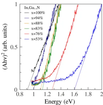
The optical band gap of our thinfilms can be determined from the PA measurements. From the signal amplitude, A, the direct band gap is determined by plotting (Ahν)2versus the photon energy, hν, and linearly extrapolating (Ahν)2to zero [8]. This is shown in figure4for all of our samples. As it can be seen in the figure, the absorption edge blueshifts with decreasing indium concentration from 0.9 eV for InN up to 1.6 eV for InGaN with x=53%.
The compositional dependence of the optical gap as measured by PA is plotted in figure 5 (full circles). It is expected that the band gap of InGaN, Eg(x), follows a
para-bolic dependence described by
E xg( ) =EInNx+EGaN(1-x)-bx(1 -x) where b is the, so-called bowing parameter, EInN and EGaNthe band gap of InN and GaN, respectively, and x the molar indium fraction. While the exact value of the bowing parameter is still not well assessed, various reviews [1, 2, 33] recommend to take b=1.43 eV [5], for the whole composition range. The compositional dependence, Eg(x), using b=1.43 eV is plot-ted infigure5as a solid line. It can be seen that the measured optical gap energy of our samples is above the expected values by ≈250 meV as a consequence of the BM shift arising from large residual electron densities, as discussed
Figure 3.Spectra of an In0.88Ga0.12N epilayer measured by different
techniques:(a) photoacoustic spectroscopy; (b) optical transmit-tance;(c) CER spectra (a successful CER spectra is shown in light gray for another InGaN sample); and (d) photoluminescence. All techniques except PA exhibit Fabry–Perot interferences.
Figure 4.PA signal of InGaN epilayers,(Ahν)2, is plotted versus photon energy. The band gap can be obtained from a linear interpolation(dashed lines).
4
below. The PL emission energies are also plotted infigure5 as crosses, which are ≈0.1 eV below the absorption edge energy measured by PA, as expected from the Stokes shift[5,6].
The high residual electron densities observed in our samples are somewhat expected since for samples with x>0.4 the Fermi stabilization energy (EFS∼4.9 eV below the vacuum level) is at a higher energy than the conduction band, which results in a large increase of electron densities arising from native defects, as accounted for by the ampho-teric defect model[34,35]. A scheme of this effect is shown in the sketch infigure5. In order to evaluate the impact of the residual electron density on the measured optical band gap, here we correct the BM shift and band gap renormalization (BGR) effects on the samples whose free electron densities were determined by Raman-scattering (in the range of (1.3–2.4)×1019
cm−3). The BM contribution has been cal-culated using a Kane’s two band k·p model [36] and assuming a non-parabolic band for InN with a momentum matrix element of EP=10 eV as reported elsewhere [37] for InN, and assuming parabolic bands for InGaN. The conduc-tion-band renormalization(BGR) effect has also been taken into account[38]. Finally, we obtained an optical gap increase of ∼150 meV including both BM and BGR effects. Despite the simplicity of the models used here for the calculation of the residual electron density and the BM shift, this value accounts for most of the discrepancy between the measured optical band gap energy and the expected compositional dependence(see solid line in figure5).
As can be seen infigure5, our BM and BGR corrected band gap values(open circles) are in perfect agreement with the measurements performed by Wu et al [5] by means of
optical absorption for samples with low electron densities(red triangles), as well as the compositional dependence of the band gap of InGaN with a bowing parameter of b=1.43 eV.
4. Conclusion
In summary, the band gap of our InGaN thinfilms has been studied by means of PL, CER, transmittance and PA. While it was not possible to obtain CER signal for indium-rich n-type InGaN, nor to successfully interpret the transmittance spectra, PA spectroscopy demonstrated to be a highly valuable tech-nique to measure the band gap of InGaN thin films. Hence, PA can be used as a valid alternative to conventional spec-troscopic methods for the measurement of the optical band gap. Moreover, we showed that the signal of PA is free of undesired Fabry–Perot interferences arising from the GaN buffer layer that are present in several spectroscopic techni-ques. From our measurements we found that a bowing parameter of b=1.43 eV successfully describes the compo-sitional dependence of the band gap of InGaN.
Acknowledgments
This work was performed within the grant of the National Science Center Poland (OPUS10 2015/19/B/ST7/02163). In addition, LJ acknowledges financial support from the National Science Center Poland (grant PRELUDIUM no. 2014/15/N/ST7/04710) and JS was supported by the stat-utory grant of WEMiF PWr no. 0401/0034/17.
ORCID iDs
Robert Oliva https://orcid.org/0000-0002-9378-4048 Robert Kudrawiec https://orcid.org/0000-0003-2593-9172
References
[1] Walukiewicz W, Ager J W III, Yu K M, Liliental-Weber Z, Wu J, Li S X, Jones R E and Denlinger J D 2006 J. Phys. D: Appl. Phys.39 R83
[2] Wu J 2009 J. Appl. Phys.106 011101
[3] Nakamura S 1998 Science281 956
[4] Feezell D F, Speck J S, DenBaars S P and Nakamura S 2013 J. Disp. Technol.9 190
[5] Wu J, Walukiewicz W, Yu K M, Ager J W III, Haller E E, Lu H and Schaff W J 2002 Appl. Phys. Lett.80 4741 [6] Schley P et al 2006 Phys. Status Solidi b243 1572
[7] Donmez O, Gunes M, Erol A, Arikan M C and Balkan N 2011 J. Appl. Phys.110 103506
[8] Zelewski S J, Kopaczek J, Linhart W M, Ishikawa F, Shimomura S and Kudrawiec R 2016 Appl. Phys. Lett.109
182106
[9] Ghosh A K, Som K K, Chatterjee S and Chaudhuri B K 1995 Phys. Rev. B51 4842
[10] Riech I, Gomez-Herrera M L, Dı́az P, Mendoza-Alvarez J G, Herrera-Pérez J L and Marı́n E 2001 Appl. Phys. Lett.79 964 Figure 5.Experimental values for the optical band gap as measured
by PL(crosses), PA before and after BM and BGR corrections (full and open circles, respectively) and those measured from absorption by Wu et al[5] (red triangles). A dashed grey line indicates the
composition(x=0.4) at which the Fermi stabilization energy (EFS)
matches the conduction band energy. The inset schematically shows the conduction bandfilling phenomena for compositions lower and higher than x=0.4.
[11] Takeda Y, Takagi D, Sano T, Tabata S, Kobayashi N, Shen Q, Toyoda T, Yamamoto J, Ban Y and Matsumoto K 2008 Japan. J. Appl. Phys.47 8805
[12] Yamaguchi A A, Nakano T, Sakai S, Fukada H and Kanitani Y 2017 Proc. SPIE10104 1010409–1
[13] Kudrawiec R 2010 Phys. Status Solidi b247 1616
[14] Schuster M, Gervais P O, Jobst B, Hösler W, Averbeck R, Riechert H, Iberl A and Stömmer R 1999 J. Phys. D: Appl. Phys.32 A56
[15] Halliwell M A G 1997 J. Cryst. Growth170 47
[16] Parker C A, Roberts J C, Bedair S M, Reed M J, Liu S X and El-Masry N A 1999 Appl. Phys. Lett.75 2776
[17] Oliva R et al 2012 J. Appl. Phys.111 063502
[18] Yeh C-Y, Lu Z W, Froyen S and Zunger A 1992 Phys. Rev. B
46 10086
[19] Pereira S, Correia M R, Pereira E, O’Donnell K P,
Trager-Cowan C, Sweeney F and Alves E 2001 Phys. Rev. B
64 205311
[20] Trainor J W and Rose K 1974 J. Electron. Mater.3 821
[21] Siozade L, Leymarie J, Disseix P, Vasson A, Mihailovic M, Grandjean N, Leroux M and Massies J 2000 Solid State Commun.115 575
[22] Hernández S, Cuscó R, Pastor D, Artús L, O’Donnell K P, Martin R W, Watson I M, Nanishi Y and Calleja E 2005 J. Appl. Phys.98 013511
[23] Cuscó R, Ibáñez J, Alarcón-Lladó E, Artús L,
Yamaguchi T and Nanishi Y 2009 Phys. Rev. B79 155210 [24] Cuscó R, Alarcón-Lladó E, Ibáñez J, Yamaguchi T,
Nanishi Y and Artús L 2009 J. Phys.: Condens. Matter21
415801
[25] Lin F, Xiang N, Wang X C, Arokiaraj J, Liu W and Chua S J 2008 J. Electrochem. Soc.155 H307
[26] Hums C, Finger T, Hempel T, Christen J, Dadgar A, Hoffmann A and Krost A 2007 J. Appl. Phys.101 033113 [27] Kudrawiec R, Siekacz M, Kryśko M, Cywiński G,
Misiewicz J and Skierbiszewski C 2009 J. Appl. Phys.106
113517
[28] Motyka M, Kudrawiec R, Syperek M, Misiewicz J,
Rudziński M, Hageman P R and Larsen P K 2007 Thin Solid Films515 4662
[29] Aspnes D E 1973 Surf. Sci.37 418
[30] Davydov V Y et al 2002 Phys. Status Solidi b230 R4
[31] Kazlauskas K, Tamulaitis G, Pobedinskas P, Žukauskas A, Springis M, Huang C-F, Cheng Y-C and Yang C C 2005 Phys. Rev. B71 085306
[32] Huang Y H, Cheng C L, Chen T T, Chen Y F and Tsen K T 2007 J. Appl. Phys.101 103521
[33] Vurgaftman I and Meyer J R 2003 J. Appl. Phys.94 3675
[34] Li S X, Yu K M, Wu J, Jones R E, Walukiewicz W, Ager J W, Shan W, Haller E E, Lu H and Schaff W J 2005 Phys. Rev. B
71 161201
[35] Wu W W J 2003 J. Appl. Phys.94 6477
[36] Kane E O 1957 J. Phys. Chem. Solids1 249
[37] Wu J, Walukiewicz W, Shan W, Yu K M, Ager J W, Haller E E, Lu H and Schaff W J 2002 Phys. Rev. B66
201403
[38] Walukiewicz W 1990 Phys. Rev. B41 10218
6

![Figure 2. Normalized Raman spectra of InGaN epilayers. The compositional dependence of the A 1 (LO) and E 2h modes is shown in the inset, together with the expected dependency (solid lines) as reported elsewhere [17].](https://thumb-eu.123doks.com/thumbv2/9libnet/5669058.113470/4.892.76.432.98.449/figure-normalized-epilayers-compositional-dependence-expected-dependency-reported.webp)