Special Issue of the 8th International Advances in Applied Physics and Materials Science Congress (APMAS 2018)
Cu Doping Induced Structural and Optical Properties of
Bimetallic Oxide Nanodots by the Vertical Spark Generation
T. Güngör
a,∗, E. Güngör
a, D. Çalışkan
band E. Özbay
baBurdur Mehmet Akif Ersoy University, Department of Energy Systems Engineering, Burdur, Turkey bBilkent University, Nanotechnology Research Centre, Ankara, Turkey
Undoped ZnO and Cu doped ZnO nanodots (NDs) were synthesized by the modified sparking technique with the Zn and Cu metal electrode pairs such as Zn–Zn, Zn–Cu and Cu–Cu. The effect of deposition geometry on the structural, optical properties and band gap energy were examined. The X-ray diffraction (XRD) analysis demonstrates that the nanodots have the hexagonal wurtzite structure, and visible considerable shift in the peaks position can be linked with the influence of Cu. However, when copper electrode was used, some copper oxide phases, metallic copper and paramelaconite phases were observed. From the results, the average diameters of metal oxide nanodots are about 25 nm and 50 nm which were obtained by using Cu–Cu and for Zn–Zn electrodes respectively from the scanning electron microscopy (SEM) analysis. When the Zn–Cu electrode pairs were used, the mixture of nanorod and nanodots appeared. It was observed that the island growth occurs in the horizontal geometry of electrode pairs and the growth metal oxide species are more strongly bonded to each other than to the substrate. But, these nanodots have more uniform distribution in the vertical geometry of electrodes. Optical studies indicated that the band gap decreased (red shift) when the Cu electrode was used.
DOI:10.12693/APhysPolA.135.857
PACS/topics: Cu:ZnO nanodots, metal oxide nanodots, spark discharge, electric discharges; semiconductor
1. Introduction
Transition metal oxides have acquired much atten-tion owing to their wide potential technological applica-tions [1–3]. In addition, the nanostructured oxides show better electronic and optical properties compared with those of the corresponding bulk materials [4–6]. For ex-ample, copper nanodots smaller than 50 nm are consid-ered super hard materials that do not exhibit the same malleability and ductility as bulk copper [7]. Among the these oxides, Zinc oxide nanodots (ZnO) are of spe-cial interest, because of electrical, optical and magnetic properties can be modify by doping. ZnO can be doped easily n-type, but the realization of stable p-type ZnO is rather difficult [8]. Whereas oxides of copper show p-type conductivity. So, Cu doped ZnO nanostructured oxides are attracting renewed interest as promising Transparent Conductive Oxide (TCO) materials in the fabrication of a wide range of optoelectronic devices. Both Cu and zinc are nontoxic, economic and abundant availability. The cuprous oxide (Cu2O, cuprite), cupric oxide (CuO,
tenorite) and Cu4O3 (paramelaconite) are the oxidized
form of copper. All three are semiconductor features. But cuprous oxide (Cu2O) and cupric oxide (CuO) are
the two main semiconductor phases of copper oxide with narrow band gap [9]. Several synthesis techniques are available for the CuO nanodots such as sol-gel, precipita-tion, thermal oxidation and microwave assisted solvother-mal method [10–12]. DC magnetron sputtering, rf mag-netron sputtering, PLD and vacuum arc plasma
evapora-∗corresponding author; e-mail: [email protected]
tion (VAPE) are also available for Cu2O. The spark
dis-charge technique, was first used by Schwyn in 1988 [13], is the one of the simple, compact, and a versatile method to produce nanodots (NDs) of different types of mate-rials. In addition, the synthesis can be performed at atmospheric pressure which is quite economic in com-parison with vacuum methods and has the potential of being scaled up. This method was used for depositing ZnO nanodots [14] and Co doped ZnO nanodots using as high purity Zn and Co metal by our group [15].
According to the synthesis techniques of copper nan-odots, it is not envisaged that copper will emerge from which phase. In order to contribute to clari-fication of the uncertainty in the phases, spark dis-charge technique in vertical geometry were used. To see the effects of Zn on the copper nanodots Zn–Zn, Zn–Cu, and Cu–Cu electrode pairs were used as the metal source. Then the optical and structural prop-erties ZnO and Cu doped ZnO nanodots on the glass substrates have been investigated.The structural and morphological properties of the films were characterized by grazing incidence X-ray diffraction (GI-XRD), scan-ning electron microscopy (SEM). The photoluminescence measurement (PL) and optical transmission measure-ments were used to obtain band gap and film thickness of the samples.
2. Materials and equipment
The metal nanodots were produced using by the spark discharge system with the vertical geometry (See refer-ence [15] for details). Two different metals such as zinc wire (Ø0.38 mm, purity 99.97%, Advent Research Ma-terials Ltd.) and copper wire (Ø0.38 mm) were used
The phase analysis has been carried out using grazing incidence X-ray diffraction (GI-XRD: Rigaku Ultima-IV; grazing angle of 0.03◦, CuKα1 X-ray source).
Composi-tional and morphological information of the samples have been gained using both Zeiss Scanning electron micro-scope (SEM) column equipped with an energy dispersive in-lens detector and a SEM (JEOL JSM-7001F) coupled with EDX (Oxford Instruments INCA Energy 350). The PL measurement was performed on a HORIBA Jobin-Yvon Triax 550 system with continuous wave He–Cd laser (325 nm) with power 100 mW as the excitation source. The optical transmittance measurements of the samples were carried out at room temperature using T70 Model Spectrophotometer (PG Instrument) in the wavelength range 300–800 nm. A special mask with 2 mm diameter was centered on the spark affected region.
3. Results and discussion 3.1. Structural properties
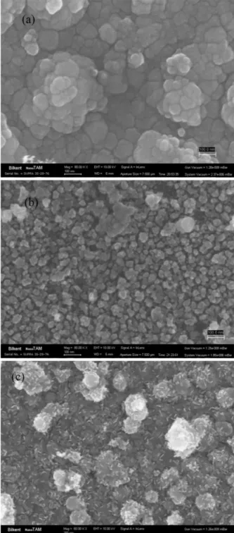
The SEM analysis was carried out at the center of the spark-affected area with a high magnification. Figure 1 shows the SEM images of undoped and Cu-doped ZnO NDs for the vertical geometry of the electrodes in spark discharge system. Among the particles examined, it was found that the surface is almost completely covered with grains (∼ 50 nm) and some of the grains are in the form of islands for Zn–Zn electrodes. However, smaller grains (∼ 25 nm) homogeneously distributed over the 95% of the average sample surface area of the Cu–Cu electrodes. ND size distributions for Zn-Zn electrodes and Cu-Cu electrodes are shown in Fig. 2a and b. However, when the Zn–Cu electrodes were used (Fig. 1c), the grains ap-pear to be double phase such as the mixture of nanowires and nanodots. The synthesized nanowires have diameters nearly 10 nm, while their average length lies in the range of 10 to 40 nm. As a result, the shape and size of Cu doped ZnO nanostructures depend on Cu. The chemical composition of the nanodots was measured using EDX. The atomic percentage of zinc and oxygen were found as 75% and 25% for pair of Zn–Zn electrodes. The atomic percentage of copper and oxygen were observed as 60%
Fig. 1. SEM pictures for metal oxide nanodot thin films by using (a) Zn–Zn, (b) Zn–Cu and (c) Cu–Cu electrode pairs, respectively.
and 40% for pair of Cu–Cu electrodes, respectively. In addition, when the Zn-Cu electrodes were used, it was obtained that Zn and Cu ions were dominant compared with the oxygen in the nanodot thin film.
The GI-XRD patterns of the prepared sample are shown in Figs. 3 and 4. The spectrum of ZnO for Zn–Zn electrode pairs shows peaks corresponding to the (100), (002), (101), (102), (110), (103), (200), (112) and (201)
Fig. 2. Nanodot diameter distribution histogram for (a) Zn–Zn and (b) Cu–Cu electrode pairs.
crystallographic planes which are match with JCPDS card data of ZnO having wurtzite type crystal structure. It is found that (002) diffraction peak is dominant and crystalline size is 22 nm.
It was clearly seen that there was also a considerable shift in (100), (002) and (101) peaks for the Cu doped ZnO NDs. This shift corresponds to the strain of the compound and replacement of some Zn2+ion with Cu2+
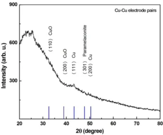
ions because of their comparable ionic radii such as 0.096, 0.072 and 0.074 nm for Cu+, Cu2+ and Zn2+, respec-tively. In addition, the peaks intensities were increased after replacing the copper electrode with Zn electrode and crystalline size calculated as 20 nm. Similar behav-ior reported in literature [16–18]. This behavbehav-ior is an indication that the shorter Cu–O bonds length than the Zn–O bonds length can be calculated using the formula given by [19]. However, The XRD analysis demonstrates that the basic structure of ZnO nanodots remains the same as hexagonal wurtzite structure and the particle size decreases for the Cu doped ZnO NDs. However, it is also found that the (111) peak is related cubic phase of copper (Fig. 3). In addition, when copper electrode pairs were used, some copper oxide phases such as (101) and (200) for CuO and (111) and (200) for metallic copper and (301) for paramelaconite were observed (Fig. 4).
Fig. 3. XRD patterns of undoped and Cu doped Zn-based oxides by using Zn–Zn (black line), Zn–Cu (red line) electrode pairs. The reference diffraction peaks were indicated by blue color.
Fig. 4. XRD pattern of Cu based oxide by using Cu– Cu (black line) electrode pairs. The reference diffraction peaks are indicated by blue color.
3.2. Optical properties
The effects of electrode materials on the optical trans-mission are shown in Fig. 5. When Zn–Zn electrodes were used in vertical geometry an optical transmittance was observed above 80% on average at wavelengths greater than 400 nm. When Zn–Cu electrodes were used, a reduction in grain size was observed. The decrease in grain size causes scattering of the light passing through the ND deposited region in which leads to a decrease in the optical transmittance. In addition, an increase in optical transmittance was observed when Cu–Cu elec-trodes were used instead of Zn–Cu elecelec-trodes. This may be due to irregularities in the structure consisted of mixed grains.
Fig. 5. Experimental and theoretical optical transmis-sion spectra are shown by lines (green line for Zn–Zn, red line for Zn–Cu and black line for Cu–Cu electrode pairs) and symbols respectively.
Taking into account the surface coated by nanodots can be accepted in the form of thin film. Hence op-tical response such as opop-tical transmittance, T (λ), can be used to determination of the thickness and optical constants with classical or iterative methods. When interference is not observed or insufficient, the classi-cal method cannot be used [20, 21]. Instead, itera-tive methods can be used [22, 23]. Thicknesses of films coated with Zn, Zn–Cu and Cu nanodots were deter-mined at around 160 nm by applying the pointwise un-constrained minimization algorithm (PUMA) onto the optical transmission spectra. There are excellent agree-ment with the experiagree-mental spectra and theoretical spectra (Fig. 5).
The optical band gap (Eg) of the semiconductor
mate-rials that is related to the optical absorption coefficient (α) and the incident photon energy (hν) by using Tauc equation [24];
hν = A(hν − Eg)n (1)
where α is absorption coefficient, A is the probability pa-rameter for the transition (independent from ν) and n the exponent that depends on the kind of optical tran-sition (n = 1/2, 2 when the trantran-sition is direct-allowed, indirect-allowed respectively).
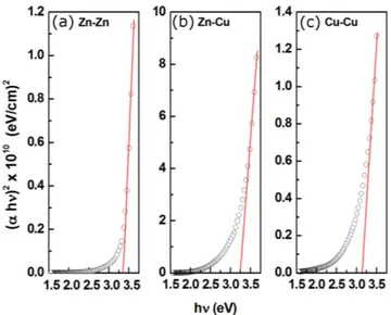
The functional relationship between (αhν)2 and
pho-ton energy for the samples can be given by Tauc plot and is presented in Fig. 6a–c. The energy gaps, ob-tained by extrapolating the linear portion to the pho-ton energy axis, are 3.35 eV, 3.24 eV and 3.14 eV for the Zn–Zn, Zn–Cu and Cu–Cu electrode pairs, respec-tively. Band gap decrease can be attributed to the substitution of Zn2+ by Cu2+ ions in the ZnO
lat-tice. In addition, the reduction in copper nanodot size that causes structural disorder in zinc oxide lattice. This behavior is in agreement with the reported studies in literature [25, 26].
Fig. 6. (αhν)2 − hν behavior of oxide nanodot thin films by using Zn–Zn (a), Zn–Cu (b) and Cu–Cu elec-trode pairs (c).
Fig. 7. PL spectra of oxide nanodot thin films by using Zn-Zn, Zn-Cu and Cu-Cu electrode pairs (a) and Cu-Cu electrode pairs (b) for different spark number (n = 100 and n = 200).
Figure 7a shows the photoluminescence spectrum of samples deposited using Zn–Zn, Zn–Cu and Cu–Cu elec-trode pairs. We can see that the luminescence of all sam-ples have a major peak is associated with near band-edge emission. The intensity of major peak located at 373 nm (3.32 eV) for Zn–Zn electrode pairs decreased with Cu ad-dition. The slight shifting in band edge peak located at 377 nm (3.29 eV) confirms the existence of doping states of ZnO due to the Zn–Cu electrode pairs. In addition, when considering the Cu–Cu electrode pairs, sample has two emission peaks at wavelengths of 390 nm and 455 nm. The first peak is well known due to radiative transition from recombination of electrons with holes in the valence band. The other peak at 455 nm can be attributed to Cu2+–Cu+ transitions (Fig. 7b). Even though the
num-ber of sparks increased, the peak intensity reduced was observed. The PL peak originating from the defect has also been observed in the literature [27–29].
4. Conclusion
Undoped ZnO and Cu doped ZnO bimetallic nanodots were successfully prepared by the spark discharge sys-tem with the vertical geometry. The Cu doping effect on the structural and optical properties of ZnO nan-odots was observed. XRD analysis shows that the ba-sic crystal structure of ZnO nanodots remains the same as hexagonal wurtzite structure. But, the structural deformation of ZnO host material in the presence of Cu2+ ions was monitored by shifting in the peak posi-tions of the ZnO structure. The average crystallite size of ZnO and Cu doped ZnO nanodots calculated from XRD patterns was 22 nm and 20 nm, respectively. The SEM images showed that the prepared Zn-Cu bimetallic nanodots consist of mixture of spherical nanodots and nanorods originated from Zn and Cu, respectively. The UV–visible spectrum of Cu doped ZnO nanodots shows a red shift compared to the ZnO and the optical trans-mittance decreased due to decreased the grain sizes. The thicknesses of the bimetallic nanodot layers coated us-ing with the Zn–Zn, Zn–Cu and Cu–Cu electrode pairs were determined as about 160 nm. PL measurements taken on Cu doped ZnO and undoped ZnO samples show that, the band-edge UV emission is red-shifted by ∼ 4 nm. The decrease in the band-edge emission can be attributed to the substitution of Zn2+ by Cu2+ ions in the ZnO lattice.
Acknowledgments
This study was supported by The Scientific and Tech-nological Research Council of Turkey with the number of project 116F046 and the Scientific Research Unit of Burdur Mehmet Akif Ersoy University with the num-ber of projects 110-NAP-10, 100-NAP-10, 172-NAP-13, 173-NAP-13, 0324-NAP-16 and 0356-NAP-16.
References
[1] D. Li, J. Hu, R. Wu, J.G. Lu, Nanotechnology 21, 485502 (2010).
[2] Y. Xu, D. Chen, X. Jiao, J. Phys. Chem. B 109, 13561 (2005).
[3] J. Huang, S.R. Wang, Y.Q. Zhao, X.Y. Wang, S.P. Wang, S.H. Wu, S.M. Zhang, W.P. Huang,Catal. Commun. 7, 1029 (2006).
[4] J.S. Bradley, in: Cluster and Colloids: From The-ory to Application, Ed. G. Schmid, Weinheim, Wi-ley/VCH, 1994, p. 459.
[5] M.S. Niasari, F. Davar,Mater. Lett. 63, 441 (2009). [6] W.K. Han, J.W. Choi, G.H. Hwang, S.J. Hong, J.S. Lee, S.G. Kang, Appl. Surface Sci. 252, 2832 (2006).
[7] Y. Suresh, G. Bhikshamaiah, A.K. Singh,AIP Con-ference Proceedings 1591, 372 (2014).
[8] A. Janotti, C.G. Van de Walle,Rep. Prog. Phys. 72, 126501 (2009).
[9] A. Das, A. Kushwaha, N.R. Bansal, V. Suresh, S. Dinda, S. Chattopadhyay, G.K. Dalapati, Adv. Mater. Lett. 7, 600 (2016).
[10] V. Usha, S. Kalyanaraman, R. Thangave, R. Vet-tumperumal, Superlattices Microstruct. 86, 203 (2015).
[11] M. Sahooli, S. Sabbaghi, R. Saboori,Mater. Lett. 81, 169 (2012).
[12] S.G. Rejith, C. Krishnan, Mater. Lett. 106, 87 (2013).
[13] S. Schwyn, E. Garwin, A. Schmidtott,J. Aerosol. Sci. 19, 639 (1988).
[14] T. Kumpika, W. Thongsuwan, P. Singjai,Thin Solid Films 516, 5640 (2008).
[15] E. Gungor, T. Gungor, D. Caliskan, E. Ozbay,Acta Phys. Pol. A 131, 500 (2017).
[16] P.D. Sahare, V. Kumar, Int. J. Innovative Technol. Exploring Eng. 3, 15 (2013).
[17] T.S. Herng, S.P. Lau, S.F. Yu, H.Y. Yang, L. Wang, M. Tanemura, J.S. Chen, Appl. Phys. Lett. 90, 32509-3 (2007).
[18] Z. Zhang, J.B. Yi, J. Ding, L.M. Wong, H.L. Seng, S.J. Wang, J.G. Tao, G.P. Li, G.Z. Xing, T.C. Sum, C.H.A. Huan, T. Wu,J. Phys. Chem. C 112, 9579 (2008).
[19] G. Srinivasan, R.T.R. Kumar,J. Sol-gel Technol. 43, 171 (2007).
[20] J.C. Manifacier, J. Gasiot, J.P. Fillard, J. Phy. E: Sci. Instrum. 9, 1002 (1976).
[21] R. Swanepoel, J. Phys. E: Sci. Instrum. 17, 896 (1984).
[22] E.G. Birgin, I. Chambouleyron, J.M. Martinez, J. Comput. Phys. 151, 862 (1999).
[23] T. Gungor, E. Gungor, B. Saka, Nanomaterials and Nanotechnology 6, 1 (2016).
[24] J. Tauc, R. Grigorovici, A. Vancu,Phys. Status Solidi 15, 627 (1966).
[25] G. Varughese1, V. Rini, S.P. Suraj, K.T. Usha, Ad-vances in Materials Science 14, 49 (2014).
[26] S. Thakur, N. Sharma, A. Varkia, J. Kumar, Adv. Appl. Sci. Res. 5, 18 (2014).
[27] A. Hausmann, B. Schallenberger, R. Roll,Z. Physik B 34, 129 (1979).
[28] D.J. Robbins, D.C. Herbert, P.J. Dean, J. Phys. C. Solid State Phys. 14, 2859 (1981).
[29] S.H. Mousavi, S.A. Jafari Mohammdi, H. Harati-zadeh, P.W. de Oliveira in:Advances in Optical Com-munication, Ed. N. Das, IntechOpen, Rijeka 2014, p. 67.