New Squarer Circuits and a Current-Mode Full-Wave
Rectifier Topology Suitable for Integration
Shahram MINAEI
1, Erkan YUCE
21 Dept. of Electronics and Communications Engineering, Dogus University, Acibadem, 34722 Kadikoy, Istanbul, Turkey 2 Dept. of Electrical and Electronics Engineering, Pamukkale University, 20017 Kinikli-Denizli, Turkey
[email protected], [email protected] Abstract. In this paper, three squarer configurations and a
current-mode (CM) full-wave rectifier circuit are sug-gested. The first and second squarer configurations re-spectively use two PMOS and two NMOS transistors while the third one employs three PMOS and one NMOS tran-sistors. A CM full-wave rectifier with high output imped-ance current is developed. All of the proposed circuits provide several advantages such as low number of compo-nents and less power consumption. The proposed circuits are simulated using SPICE program to demonstrate their performance and workability.
Keywords
CMOS, squarer circuit, rectifier, current-mode.
1. Introduction
MOS-based analog squarer circuits may have voltage inputs and current outputs, and find wide application areas such as neural and image processing [1]. Recently, a squarer topology using a number of CMOS transistors has been reported [2]. Apart from these, it is well-known that a current-mode (CM) approach offers certain potential advantages such as higher usable gain, greater linearity, lower power consumption, wider bandwidth, lower num-ber of components and larger dynamic range when com-pared to its voltage-mode (VM) counterpart [3]-[5]. CM and VM full-wave rectifiers are widely used in analog signal processing, analog communication systems, condi-tioning and instrumentation of low-level analog signals as well as dc converters. However, only a few CM rectifiers were previously published in the open literature [6]-[10].
In this paper, three new circuits for providing squared analog output currents are proposed. All of the introduced squarer structures are simple, and dissipate less power when compared to that of [2] because of the fact that two of the proposed squarer circuits use only two MOS tran-sistors while the other one employs four MOS trantran-sistors. Further, all of the squarer circuits operate in class B. A full-wave rectifier circuit employing only six MOS
tran-sistors dissipating less power is also introduced. Contrary to the CMOS-based CM rectifiers given in [7]-[10], the developed CM rectifier can provide gain at output current. However, all the developed circuits need bias voltages which can be obtained by bias voltage generators.
The rest of the paper is organized as follows. The proposed squarer circuits are presented in Section 2. A simple CMOS-based CM full-wave rectifier is given in Section 3. The simulation results of the introduced circuits based on SPICE program are given in Section 4 and finally some concluding remarks are drawn in Section 5.
2. Proposed Squarer Circuits
The drain current of a long-channel PMOS/NMOS transistor operating in saturation region can be respectively given by the square-law relation as:
2 ) ( 2 1 TP SG p D k V V I , (1) 2 ) ( 2 1 TN GS n D k V V I (2)
where kp =pCox(W/L) and kn =nCox(W/L), p and n are
respectively surface mobilities of PMOS and NMOS tran-sistors, Cox is the gate capacitance per unit area, and W/L is
the aspect ratio (channel width/channel length) of the tran-sistor [11]. The threshold voltages VTP and VTN are
respec-tively expressed as
Fn BS Fn
p TP TP V V V 0 2 2 , (3.a) TN n Fp SB Fp TN V V V 0 2 2 (3.b)where VTP0 (VTN0) is the threshold voltage with VSB=0
(VBS=0), 2Fn (2Fp) is the bulk surface potential and p (n)
is the body-effect coefficient of the PMOS (NMOS) tran-sistor. Note that 2Fn and n are positive while 2Fp and p
are negative.
The introduced squarer circuits with two PMOS/NMOS transistors are shown in Figs. 1 and 2, respectively. If the input voltage signal in Fig. 1 is in
positive cycle, M1 is OFF while M2 operates in saturation region. Here VTP are the dc bias voltages. Likewise, if the input is in negative cycle, M2 is OFF and M1 operates in saturation region. For the circuit of Fig. 2 which is biased with VTN voltages, if the input voltage signal is in positive cycle, M3 is OFF while M4 operates in saturation region. Similarly, if the input signal is in negative cycle, M4 is OFF and M3 operates in saturation region.
Fig. 1. The proposed PMOS-based squarer circuit.
Fig. 2. The proposed NMOS-based squarer circuit.
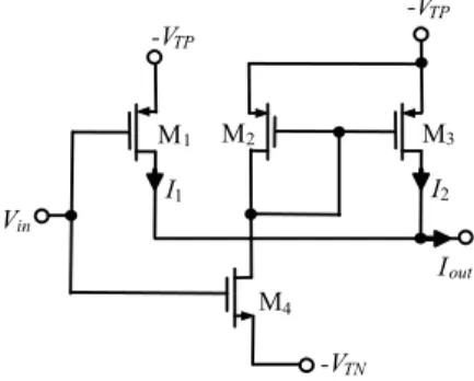
I1 Vin M4 M1 M2 I2 M3 -VTN Iout -VTP -VTP
Fig. 3. The proposed CMOS squarer circuit.
The output of the PMOS squarer of Fig. 1 and NMOS squarer of Fig. 2 can be normally connected to, respec-tively, NMOS and PMOS current mirrors, or can be grounded. Assuming MOS square-law characteristic for the MOS transistors, the output currents of the squarer topolo-gies given in Figs. 1 and 2 can be respectively evaluated as
2 out1 2 1 in pV k I , (4) 2 out2 2 1 in nV k I . (5)
Here kp1 = kp2 = kp and kn3 = kn4 = kn. Another squarer
configuration is given in Fig. 3, which has high input and output impedances resulting easy cascadability with other circuits. The output current of the squarer topology given in Fig. 3 is evaluated as 2 2 1 in out kV I . (6)
Here, k=kn4 =kp1. Moreover unity current gain is
as-sumed for the current mirror composed of transistors M2 and M3 (kn2 =kp3) to ensure equal cycles at the output
cur-rent. Considering mismatch between bias voltages and threshold voltages of the transistors, the output current of the squarer topology given in Figs. 1-3 can be expressed as
otherwise 2 2 2 1 V 2 1 0 V 2 1 in in in out V k V V k I (7)In (7), undesired components, ∆V1 and ∆V2, are voltage differences between corresponding bias voltages and threshold voltages. The output current, Iout, in (7) can
be rewritten as otherwise 0 1 2 2 0 1 2 2 0 b V b V b V a V a V a I in in in in in out (8)
where a1, b1, a0 and b0 given below are ideally equal to zero. . V 2 , V 2 , V , V , 2 2 2 0 2 1 0 2 1 1 1 2 2 k b k a k b k a k b a (9)
If ∆V1 and ∆V2 in (9) are set to zero, the suggested circuits have approximately zero dc current yielding very low power dissipation. In other words, the developed squarer structures can ideally be operated in class B mode.
For providing the bias voltages required in the proposed squarer circuits, one can use the biasing circuit topologies described in [12]. As an example the following relationships can be written for the biasing circuit shown in Fig. 4.
2 TN2 2 2 2 TN 1 1 V 2 1 V 2 1 kn VDS kn VDS I , (10) DD DS DS V V V 1 2 . (11)The output voltage of the circuit in Fig. 4 is found as ) V -( V TN2 2 1 2 TN1 2 1 1 DD n n n n n n o V k k k k k k V . (12)
If kn1>>kn2 thus Vo VTN1. Thus the circuit of Fig. 4
can be used to extract the threshold voltage VTN.
Alterna-tive circuits for extracting VTN and VTP voltages can be
found in [13], [14].
3. Current-Mode Rectifier
In this section a new CMOS-based CM full-wave rectifier is proposed as shown in Fig. 5. If the CM input signal is in the positive cycle, M1 and M2 are OFF while others are in saturation region; thus, the input signal is transferred from the transistors M5, M6, and M3 to the tran-sistor M4 in the same direction as Irect+ Similarly, if the input signal is in the negative cycle, transistors M3, M4, M5 and M6 are OFF while M1 and M2 operate in saturation region; accordingly, this signal can pass in the opposite sign from M2( Irect-). The output current which can be ob-tained by connecting Irect+ and Irect- together is calculated as follows:
in
out I I I
I rect rect . (13)
Here Irect+ andIrect- are respectively defined as
0 otherwise 0 rect in in I I I (14) otherwise 0 0 -rect in in I I I (15)
It is important to note that by changing the aspect ratios of M2 and M4, the magnitude of Iout in (13) can be set
to any value. In other words, the output current in (13) can be given as
aIrect bIrect
Iout (16)
where, a and b are positive real numbers whose values depend on the aspect ratios of CMOS transistors of Fig. 5.
-VTP M1 I rect-Iin M5 M6 M2 M3 Irect+ M4 -VTN -VTP
Fig. 5. Developed CMOS-based current-mode full-wave rectifier circuit.
4. Simulation Results
In this section, simulation results of the proposed circuits obtained through SPICE program using BSIM 3v3,
0.18 m TSMC CMOS technology parameters
(VTN0= 0.3725 V, VTP0= 0.3948 V, 0N= 259.53 cm2/V-s,
0P= 109.976 cm2/V-s, TOX= 4.1 nm), are given. Aspect
ratios of MOS transistors of the squarer circuits are given in Tab. 1. PMOS Transistors W(m)/L(m) M1 9.54/1.08 M2 8.64/1.08 NMOS Transistors W(m)/L(m) M3 3.6/1.08 M4 3.78/1.08
Tab. 1. Dimensions of the transistors used for the squarer circuits of Figs. 1 and 2.
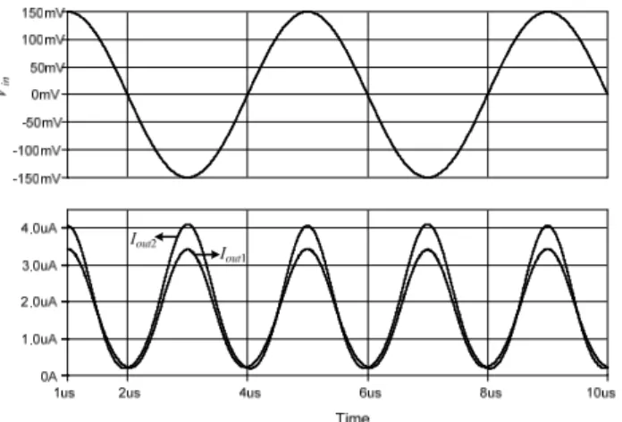
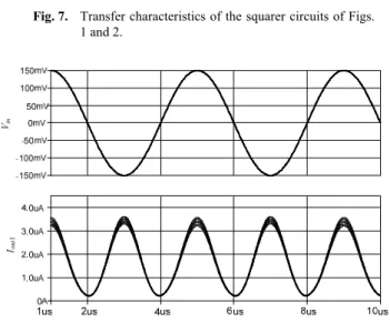
A sinusoidal voltage signal with 150 mV peak value at 250 kHz is applied to the inputs of the developed squarer topologies in Figs. 1 and 2 to obtain the squared output currents as shown in Fig. 6. The input-output transfer char-acteristics of the proposed squarer circuits are depicted in Fig. 7. As it can be seen from the characteristics shown in Fig. 7, a subthreshold current of approximately 200 nA flows through the transistors for zero input voltage. Addi-tionally, the total power dissipations of the circuits in Figs. 1 and 2 (excluding biasing circuitry) are found approxi-mately equal to 0.08 µW. The circuit of Fig. 1 is selected as an example to demonstrate the transistor mismatch ef-fects on the performance of the squarer. The channel widths of the transistors M1 and M2 in Fig. 1 are changed respectively from 9.18 µm to 10.08 µm and 8.1 µm to 9 µm by 0.18 µm increments. The resulted output waveforms are shown in Fig. 8.
Fig. 6. Output currents of the squarer circuits of Figs. 1 and 2.
Aspect ratios of CMOS transistors in the rectifier cir-cuit of Fig. 5 are given in Tab. 2. A CM sinusoidal signal with 20 A peak value at 1 MHz is applied to the input of the developed rectifier depicted in Fig. 5 to obtain the
full-wave rectified output current as shown in Fig. 9. In addi-tion the output current of the suggested rectifier against the applied input current is drawn in Fig. 10. Note that the proposed rectifier can operate well up to 20 MHz.
Iout2 Iout1 Vin -200mV -100mV 0V 100mV 200mV 0A 2.0uA 4.0uA 6.0uA 8.0uA 10.0uA
Fig. 7. Transfer characteristics of the squarer circuits of Figs. 1 and 2.
Fig. 8. Input voltage and output current waveforms of the squarer circuit of Fig. 1 under transistor mismatch.
It is seen from Figs. 6-10 that the simulation results are in good agreement with theoretical ones as expected. However, the slight discrepancy between ideal and simula-tion output currents of the proposed squarer and rectifier circuits mainly arises from the non-idealities of the CMOS transistors. PMOS Transistors W(m)/L(m) M1 and M3 10.8/0.18 M2 12.06/0.18 M4 15.48/0.18 NMOS Transistors W(m)/L(m) M5 and M6 3.6/0.18
Tab. 2. Dimensions of the transistors used for the rectifier topology of Fig. 5.
Time
10us 11us 12us 13us 14us 15us
-20uA -10uA 0uA 10uA 20uA Iin Iout
Fig. 9. Input and output currents of the rectifier circuit in Fig. 5.
Fig. 10. Input-output characteristic of the proposed current-mode full-wave rectifier circuit.
5. Conclusion
In this paper new squarer and CM rectifier circuits are presented. The introduced CMOS-based squarer and recti-fier circuits are simple, and consume low power; accord-ingly, they are suitable for integrated circuit technology. Simulation results using SPICE program with 0.18 m TSMC CMOS technology parameters verify the theory well as desired.
References
[1] FIKOS, G., SISKOS, S. Analogue CMOS vector normalisation circuit. Electronics Letters, 1999, vol. 35, no. 25, p. 2197-2198. [2] LOPEZ-MARTIN, A. J., RAMIREZ-ANGULO, J., CHINTHAM,
R., CARVAJAL, R. G. Class AB CMOS analogue squarer circuit. Electronics Letters, 2007, vol. 43, no. 20, p. 336-338.
[3] WILSON, B. Recent developments in current conveyors and current-mode circuits. IEE Proceedings Circuits, Devices and Systems, 1990, vol. 137, no. 2, p. 63-77.
[4] TOUMAZOU, C., LIDGEY, F. J., HAIGH, D. G. Analog IC Design: The Current-Mode Approach. London: Peter Peregrinus, 1990.
[5] ROBERTS, G. W., SEDRA, A. S. All current-mode frequency selective circuits. Electronics Letters, 1989, vol. 25, no. 12, p. 759-761.
[6] BIOLEK, D., HANCIOGLU, E., KESKIN, A. U. High-performance current differencing transconductance amplifier and its application in precision current-mode rectification. AEU-International Journal of Electronics and Communications, 2008, vol. 62, no. 2, p. 92-96.
[7] WANG, Z. Novel pseudo RMS current converter for sinusoidal signals using a CMOS precision current rectifier. IEEE Transactions on Instrumentation and Measurement, 1990, vol. 39, no. 4, p. 670-671.
[8] RAMIREZ-ANGULO, J., CARVAJAL, R. G., TOMBS, J., TORRALBA, A. Very low-voltage class AB CMOS and bipolar precision current rectifiers. Electronics Letters, 1999, vol. 35, no. 22, p. 1904-1905.
[9] CHANG, C.-C., LIU, S.-I. Current-mode full-wave rectifier and vector summation circuit. Electronics Letters, 2000, vol. 36, no. 19, p. 1599-1600.
[10] WILSON, B., MANNAMA, V. Current-mode rectifier with improved precision. Electronics Letters, 1995, vol. 31, no. 4, pp. 247-248.
[11] SEDRA, A. S., SMITH, K. C. Microelectronic Circuits. Fifth edition. New York: Oxford University Press, 2004.
[12] MALOBERTI, F. Analog Design for CMOS VLSI Systems. Boston: Kluwer Academic Publishers, 2001, p. 197-198.
[13] MANARESI, N., FRANCHI, E., GNUDI, A., BACCARANI, G. MOSFET threshold extraction circuit. Electronics Letters, 1995, vol. 31, no. 17, p. 1434-1435.
[14] CILINGIROGLU, U., HOON, S. K. An accurate self-bias threshold voltage extractor using differential difference feedback amplifier. In IEEE International Symposium on Circuits and Systems. Geneva (Switzerland), 2000, vol. 5, p. 209-212.
About Authors …
Shahram MINAEI received the B.Sc. degree in Electrical and Electronics Engineering from Iran University of Sci-ence and Technology, Tehran, Iran, in 1993 and the M.Sc. and Ph.D. degrees in Electronics and Communication Engineering from Istanbul Technical University, Istanbul, Turkey, in 1997 and 2001, respectively. He is currently a Professor at the Department of Electronics and Com-munication Engineering, Dogus University, Istanbul, Turkey. He has more than 80 publications in scientific journals or conference proceedings. His current field of research concerns current-mode circuits and analog signal processing.
Dr. Minaei has served as a reviewer for several interna-tional journals and conferences. He is a senior member of the IEEE, an associate editor of the Journal of Circuits, Systems and Computers (JCSC), and an area editor of the International Journal of Electronics and Communications (AEÜ).
Erkan YUCE was born in 1969 in Nigde, Turkey. He received the B.Sc. degree from the Middle East Technical University, the M.Sc. degree from Pamukkale University and the PhD. degree from Bogazici University all in Elec-trical and Electronics Engineering in 1994, 1998 and 2006, respectively. He is currently an Assistant Professor at the Electrical and Electronics Engineering Department of Pa-mukkale University. His current research interests include analog circuits, active filters, synthetic inductors and CMOS based circuits. He is the author or co-author of about 80 papers published in scientific journals or confer-ence proceedings.