High power gain for stimulated Raman amplification in CuAlS2
B. H. Bairamov, A. Aydinli, I. V. Bodnar’, Yu. V. Rud’, V. K. Nogoduyko, and V. V. Toporov
Citation: Journal of Applied Physics 80, 5564 (1996); doi: 10.1063/1.363820 View online: https://doi.org/10.1063/1.363820
View Table of Contents: http://aip.scitation.org/toc/jap/80/10
Published by the American Institute of Physics
Articles you may be interested in
Chemistry of defect induced photoluminescence in chalcopyrites: The case of
Journal of Applied Physics 109, 023519 (2011); 10.1063/1.3544206
Band structure, Born effective charges, and lattice dynamics of from ab initio calculations
The Journal of Chemical Physics 117, 2726 (2002); 10.1063/1.1489993
Optical properties of
Journal of Applied Physics 88, 1923 (2000); 10.1063/1.1305858
Photoluminescence studies in CuAlSe2 epilayers grown by low-pressure metalorganic chemical-vapor deposition
High power gain for stimulated Raman amplification in CuAlS
2 B. H. Bairamova)and A. AydinliBilkent University, Department of Physics, Bilkent, Ankara, 06533 Turkey I. V. Bodnar’, Yu. V. Rud’, V. K. Nogoduyko, and V. V. Toporov A. F. Ioffe Physico-Technic Institute, Russian Academy of Sciences, 194021 Russia ~Received 22 February 1996; accepted for publication 11 July 1996!
The spontaneous Raman spectra of the chalcopyrite structure crystal CuAlS2, which is promising
for nonlinear optical applications, has been investigated at 8 and 300 K. The main aim of this study
is to compare the absolute spontaneous Raman scattering efficiency in CuAlS2crystals with that of
their isomorphous analog, zinc-blende structure GaP crystals, known as one of the most efficient materials for Raman amplification. Observation of a high value of absolute scattering efficiency
S/L dV ~where S is the fraction of incident power that scatters into the solid angle d V and L is the
optical path length with S/L dV59.531025cm21sr21!, together with relatively narrow linewidth
~G55.1 cm21, full width at half maximum at room temperature and G51.5 cm21 at 8 K for the
strongestG1phonon mode of CuAlS2at 314 cm21! indicate that CuAlS2has the highest value of the stimulated Raman gain coefficient gs/I where I is the incident laser power density. The calculated
value of this gain is gs/I52.131026cm21/W at 300 K and 5.031026cm/W, at 8 K for 514.5 nm
laser excitation, and is larger than those for the appropriate vibrational modes of various materials
~including GaP, LiNbO3, Ba2NbO5O15, CS2, and H2! investigated so far. The calculations show that
cw Raman oscillator operation in CuAlS2 is feasible with low power threshold of pump laser.
© 1996 American Institute of Physics.@S0021-8979~96!03020-4#
I. INTRODUCTION
Recently, a great deal of interest has been focused on the
growth of the ternary I–III–VI2and II–IV–V2
semiconduc-tor compounds which crystallize in the chalcopyrite
~CuFeS2!-type structure. Within this family there are many ternary compounds which have a band gap of in the range of 3.5–1.0 eV covering the wide spectral region from ultravio-let to near infrared and having different attractive linear and nonlinear optical properties. The usefulness of these com-pounds as nonlinear optical components owing to their high
nonlinear susceptibilities ~which are comparable to or even
greater than those of their many binary zinc-blende structure
analogs! and especially to the uniaxial birefringence ~which
makes it possible for phase matching!, is well known.
For example, zinc germanium diphosphide ~ZnGeP2!
and cadmium germanium diarsenide ~CdGeAs2! crystals are
promising candidates for efficient second harmonic
generators1 as well as mid-infrared optical parametric
oscillators2,3exhibiting very high energy conversion efficien-cies~up to 46%!, at moderate average power levels.4Another famous member of this family is silver gallium disulfide
~AgGaS2! with Eg52.7 eV ~at room temperature! which is
an important material due to its large nonlinear optical coef-ficients and birefringence.5
Due to the observation of the direct band gap for these
compounds6with chalcopyrite-type structure, one can expect
their potential applications for optoelectronic devices such as light emitting diodes and laser diodes operating in the blue and ultraviolet wavelength region.
The chalcopyrite-type semiconductor copper indium
dis-elenide ~CuInSe2! has Eg51.0 eV ~at room temperature!
which is in the energy range for optimum solar energy
con-version with the absorption coefficient of about 531025
cm21~near the band gap for polycrystalline thin films! which is the highest value reported for any semiconductor up to now.7–9
In addition, device applications of chalcopyrite-type semiconductor compounds through the formation of efficient near lattice matched heterojunctions with the semiconductor III–V and II–VI compounds is also under consideration.
As mentioned previously, the chalcopyrite-structure compounds are close isoelectronic analogs of zinc-blende structure binary semiconductors where replacement of cat-ionic sublattice by different atomic species induces a change from Td2(F4¯3m), characteristic of zinc-blende structure to the tetragonal space group D2d12(I4¯2d) characteristic for chalcopyrite structure with so-called weak tetrahedral distor-tion and tetragonal compression of anions with respect to the ideal zinc-blende structure. Therefore, the vibrational and electrical properties of chalcopyrite-type compounds have striking analogues with their II–VI and III–V homologies.
One of the promising chalcopyrite-type semiconductors for nonlinear optical applications is copper aluminum disul-fide ~CuAlS2!, which has a direct gap of 3.49 eV at room temperature, the widest value among other chalcopyrite com-pounds. Recent progress in the growth of undoped and doped bulk10as well as the heteroepitaxial growth of CuAlS2layers on ~100! GaP and ~100! GaAs substrates by metalorganic
vapor phase epitaxy11 and molecular beam epitaxy12 makes
them even more technologically promising.
As a matter of fact, the nature and origin of the high nonlinear optical susceptibility and Raman scattering effi-ciency are closely interrelated. It should be pointed out that the nonlinear optical properties of the insulating crystals are derived from both: first, the perturbation of the optical
izability by an electromagnetic field acting through a lattice displacement—so-called lattice or deformation potential in-teraction and second, the perturbation of the optical polariz-ability produced by the direct action of the field on the
elec-tronic levels—so-called nonlattice or electro-optic
interaction. The same interactions manifest themselves in the process of spontaneous Raman scattering by lattice vibra-tions.
For piezoelectric crystal structures, which lack a center
of inversion, Loudon13 has showed that both deformation
potential and electro-optic interactions contribute to the Ra-man scattering efficiency for zone center longitudinal optical
@LO~G!# modes, but that only the lattice interaction
contrib-utes to the scattering efficiency for transverse optical
@TO~G!# modes. Therefore, the measurements of absolute
scattering efficiency and linewidth of the phonon modes can permit a determination of available power gain coefficient for stimulated Raman scattering amplification.
Previously, the high value of absolute scattering
effi-ciency for the LO~G! phonon from spontaneous Raman
scat-tering intensity measurements of binary undoped GaP14 has
been observed. This, together with the observed anomalously narrow spectral linewidth, indicates a large gain coefficient for stimulated Raman scattering. The measured value of this gain was quite large by comparison with other materials, and
a low threshold of pump laser power had been predicted.15
Recently, the low threshold pump power Raman laser based on GaP and suitable for applications in optical com-munication systems in terahertz frequency region has been
demonstrated.16,17In this connection, the knowledge of the
absolute spontaneous Raman scattering efficiency and gain
coefficient for stimulated Raman scattering of CuAlS2
crys-tals and their direct comparison with those of GaP cryscrys-tals is of considerable interest. To our knowledge those
measure-ments for CuAlS2 have not been reported so far.
In the present study, an attempt has been made to find out the relationship between the spontaneous scattering
in-tensity of CuAlS2 and GaP crystals with the main aim of
determining the nonlinear Raman power gain amplification
for the strongest phonon modes of CuAlS2 for stimulated
Raman scattering process. It is found that this gain exceeds those reported for any other promising materials widely used for stimulated Raman scattering operation.
II. EXPERIMENTAL PROCEDURES
The single crystal samples used in this experiment were grown by the chemical vapor transport method in an evacu-ated quartz tube using iodine as a transport agent followed
by directional freezing. The starting polycrystalline CuAlS2
compounds were prepared by direct melting of the constitu-ent elemconstitu-ents of high quality in stoichiometric amounts. The
CuAlS2crystals were light green in color. Typical
morphol-ogy of platelike crystals showed a well developed surface
along@111# axis, with @101# and @112# facets, which are
par-allel to the axis. The typical dimensions of the grown crystals
were about 53330.4 mm3.
The crystallographic parameters obtained on our samples by using x-ray diffraction techniques carried out at room temperature with Debye–Scherrer powder method confirmed that a single phase growth with chalcopyrite structure is
achieved with a55.3336 Å and c510.440 Å. These values
are in good agreement with the parameters previously re-ported by Brandt et al.18
The measurements of spontaneous Raman scattering spectra were performed in the backscattering configuration for crossed and parallel polarization of incident and scattered
light from the naturally grown @112# plane, which
corre-TABLE I. Comparison of frequenciesn~in cm21! of the Raman and infrared active zone center optical phonons in CuAlS2with their symmetry assignment and zinc-blend origin. The splitting of polar modes with nonzero
dipole moments into transverse and longitudinal modes is also shown.
Chalcopyrite mode symmetry Zinc-blende mode symmetry Raman scat.a,b T5300 K Infrared reflectivitya,b /absorptiona,b T5300 K Raman scat. present work T5300 K T58 K G5(L,T) ~X5!ac 76/76 75.5/74.0 77.4 G3 ~W2!ac 98 96 ••• G4(L,T) ~W2!ac 112/112 108 ••• G5(L,T) ~W4!nc 137/137 135 ••• G5(L,T) ~W3! 217/216 217/216 217.5/217.5 219.5 G3 ~X3! 268 263 266.5 G5(L,T) ~X5!opt 266/263 266/263 263/261 275/265 G4(L,T) ~W2!opt 284/271 284/271 2/272 2/274 G1 ~W1! 315 314 317 G5(L,T) ~W4!opt 2/432 2/432 ••• ••• G3 ~W2!opt 443 442 448 G5(L,T) G15 497/444 497/444 496/444 498/449 G4(L,T) G15 498/446 498/446 498/446 503/448 Second-order 123 ••• features 372 ••• 553 ••• aReference 21. bReference 22. 5565 J. Appl. Phys., Vol. 80, No. 10, 15 November 1996 Bairamovet al.
sponds to the ~111! plane of zinc-blende structure material.
Both 514.5 and 476.5 nm lines of an Ar1laser, which are far
from resonance with Eg of CuAlS2 were used as the
excita-tion sources. The scattered light was analyzed using a Jobin– Yvon U 1000 double grating monochromator with a spectral
resolution of 0.9–1.1 cm21and detected with a cooled GaAs
photomultiplier operating in the photon counting mode. All measurements were performed at room temperature and at 8 K using a closed-cycle cryostat.
For the measurement of absolute scattering efficiency,
we used a zinc-blende structure semi-insulating ~si! GaP
crystal oriented along ~111! direction. Backscattering
mea-surement from the~111! face performed under the same
ex-perimental conditions as from CuAlS2 crystal. For absolute
frequency calibration, we used a Ne spectral lamp.
III. RESULTS AND DISCUSSION
As already said, the AIBIIICVI2chalcopyrite structure has the symmetry D2d12(I4¯2d) and the body centered tetragonal unit cell. For ideal chalcopyrite crystals the long dimension c must be twice the cubic length a. In our case, the structural
parameter is h5(c/2a)50.980 This value is very close to
h51 among all chalcopyrite-type compounds. The mean
tet-rahedral distortion of anions with respect to ideal zinc-blende position changes the first-nearest-neighbor interatomic
dis-tances dACand dABwhich can be characterized by parameter
u given by n2145~dAC
2 2d BC
2 !a2. ~1!
For CuAlS2, dAC52.351 Å and dBC52.239 Å and
u50.2547 Å. For comparison, analogous parameters for
other chalcopyrite-type compounds are h51.004, u50.224
Å for CuInSe219andh50.896, u50.27 for AgGaSe220which
indicate much larger structure modifications than CuAlS2.
Due to the fact that there are two different types of cations in chalcopyrite structure compounds and because their unit cell volume is four times smaller than in a typical zinc-blende material, there is a four-to-one correspondence between the Brillouin zones of the chalcopyrite and zinc-blende structure compounds. Therefore, the chalcopyrite structure semicon-ductors may be regarded as a superlattice of the zinc-blende-FIG. 1. The overall Raman spectrum of CuAlS2obtained at room
tempera-ture in the backscattering configuration from~112! plane for parallel polar-izations of incident and scattered light. The excitation wavelength is 514.5 nm and spectral resolution 0.9 cm21. Notice the large intensity ofG1phonon
mode at 314 cm21. Small peak at 329 cm21is from Ne reference lamp.
FIG. 2. Raman spectrum of CuAlS2obtained at room temperature in the
backscattering configuration from~112! plane for parallel polarizations of incident and scattered light in expanded scale in the range 150–400 cm21. The excitation wavelength is 457.9 nm and spectral resolution 1.1 cm21.
FIG. 3. Raman spectrum of CuAlS2 obtained at room temperature in the
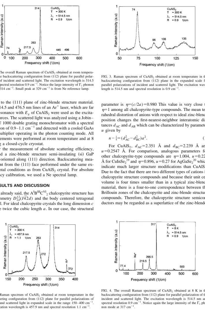
backscattering configuration from ~112! plane in the expanded scale for parallel polarizations of incident and scattered light. The excitation wave-length is 514.5 nm and spectral resolution is 0.9 cm21.
FIG. 4. The overall Raman spectrum of CuAlS2obtained at 8 K in the
backscattering configuration from~112! plane for parallel polarization of the incident and scattered light. The excitation wavelength is 514.5 nm and spectral resolution 0.9 cm21. Notice again the large intensity of theG1
type semiconductors with folding of all Brillouin zone edge
points labeled X(0,0,2p/a), W(0,2p/a,p/a) and W(2p/
a,0,p/a) back to the center of the Brillouin zone with zone
center~G-like! representations. Since the chalcopyrite struc-ture compounds have two formula units with eight atoms per unit cell, giving rise to 21 optical and three acoustic branches of lattice vibrations, the representation,G at the center of the zone, is reducible into
G51G112G213G313G416G5 and 1G411G5,
respectively. With the splitting of infrared active modes by the macroscopic long range electrostatic interaction into
transverse and longitudinal components as well as theG4and
G5 optical modes and since the G2 modes are silent, one
expects 22 Raman-active optical modes
1G113G313G4~LO!13G4~TO!16G5~LO!16G5~TO!. The symmetry types of the Raman-active modes for chalcopyrite-type structure crystals with corresponding zinc-blende structure modes are listed in Table I.
Previously, the vibrational spectra of CuAlS2 by zone
center optical phonons have been investigated at room
tem-perature by Raman scattering as well as by infrared
absorp-tion and reflectivity measurements by Koshell et al.21,22 In
addition to the already known phonon modes of CuAlS2 at
T5300 K, we describe here corrections of previous
measure-ments and assignmeasure-ments of newly observed lines.
Figure 1 shows the overall Raman scattering spectrum of
CuAlS2obtained at room temperature in the frequency range
of 0–600 cm21. The most interesting feature of this spectrum
is the large intensity of the G1 phonon mode at 314 cm21.
Other Raman lines are also revealed, but their intensities are several times smaller. Figures 2 and 3 show the Raman scat-tering spectra of those lines in expanded scales for frequency
ranges of 150–400 and 50–150 cm21, respectively. One can
easily see the appearance of new structures at 123, 272, and 372 cm21.
In order to resolve the observed broad structures and to distinguish between first and second order scattering
struc-tures at 263, 442.5, and 553 cm21, we have performed
Ra-man measurements at 8 K. The overall spectra obtained in FIG. 5. Raman spectrum of CuAlS2obtained at 8 K in backscattering
con-figuration from~112! plane for parallel polarizations of incident and scat-tered light. The excitation wavelength is 514.5 nm and spectral resolution is 0.9 cm21.
FIG. 6. Raman spectrum of CuAlS2obtained at 300 and 8 K in
backscatter-ing configuration from~112! plane for crossed polarizations of incident and scattered light. Notice the G5~LO,TO! phonon mode at 442.5 cm21 and
disappearance of second-order structure at 553 cm21. The excitation wave-length is 514.5 nm and spectral resolution is 0.9 cm21.
FIG. 7. Raman spectrum of CuAlS2obtained at 8 K in backscattering
con-figuration from ~112! plane for parallel polarizations of incident and scat-tered light. The excitation wavelength is 514.5 nm and spectral resolution is 0.9 cm21.
FIG. 8. Room temperature Raman spectrum of CuAlS2 obtained in the
backscattering configuration from~112! plane for parallel polarization of the incident and scattered light and of si–GaP obtained also in the backscatter-ing configuration from ~111! plane for identical experimental conditions including the same incident power of 2 mW and detection intensity scale. Notice the large absolute scattering intensity ofG1phonon mode at 314
cm21in comparison with LO~G! phonon mode at 402.3 cm21of Si–GaP.
5567 J. Appl. Phys., Vol. 80, No. 10, 15 November 1996 Bairamovet al.
the range 0–600 cm21 is given in Fig. 4, while the spectra obtained in expanded scales are presented in Figs. 5 and 6. With the same aim, we display in Fig. 7 the Raman spectra
of CuAlS2obtained at room temperature and 8 K in the range
400–600 cm21.
In Table I we summarize the results of our measure-ments compared to previous Raman as well as infrared ab-sorption, and reflectivity, measurements.
For the broad line observed at room temperature at 442
cm21 with structures from both sides of this line, we have
found at 8 K the appearance of two new lines centered at 442.5 and 448.5 cm21, respectively. For the other broad line
at 494 cm21at T5300 K with asymmetric structure from the
high frequency side we found a single sharp line at 503
cm21. The other very broad structure at 553~at T5300 K!
disappeared at 8 K.
It is interesting to note that theG1phonon mode always dominates the Raman spectra of all chalcopyrite structure semiconductors.19–25It appears in the spectra for all scatter-ing configurations used.
The high scattering intensity and narrow linewidth of the
G1mode in CuAlS2indicate a high value of gain for Raman
oscillator operation in the process of stimulated Raman scat-tering.
The power gain coefficient gs/I, where I is the laser
pump power per unit area for the stimulated Raman scatter-ing and for the Stokes wave, was given by Shen and
Blombergen.26 By taking into account corrections given by
Johnston and Kaminow27
gs I 5 16p2c2 hvs3 S/L dV nins~n011!G. ~2!
Here,vs is the frequency of the scattered light at the Stokes
frequency, ni and ns are refractive indices at the incident
laser and scattered Stokes frequencies, n0is the Bose
popu-lation factor, @exp~hv/kT!21#21, andG is the linewidth full
width at half maximum~FWHM! of a mode.
The power at the Stokes frequency increases with length
L as exp(gsL). Thus available power gain for stimulated
Raman scattering amplification can be obtained from the measurement of the absolute scattering efficiency. The strength of a given Raman-active phonon mode in the pro-cess of spontaneous scattering is given by the absolute scat-tering efficiency S/L dV where S is the fraction of the
inci-dent laser power that is scattered into a solid angle of dV
near a normal to the optical path L.
The efficiency of an unknown spectral mode can be ob-tained by comparison with integrated scattering intensities
~areas under spectral lines! of measured and reference
samples under identical experimental conditions.
To measure the absolute scattering efficiency ofG1mode in CuAlS2, we used as reference the scattering efficiency of
the LO~G! phonon line in semi-insulating GaP crystals
~where plasmon–phonon interaction play no role!.15 Figure 8 shows the room temperature Raman spectrum
of CuAlS2obtained in the backscattering configuration from
~112! plane for parallel polarizations of incident and
scat-tered light and for si–GaP obtained for identical experimen-tal conditions. One can see the large absolute scattering
ef-ficiency of G1 phonon mode in CuAlS2 at 314 cm21 in
comparison with that of@LO~G!# phonon mode of si–GaP at
402.3 cm21. The calibrated ratio of the areas under these two
spectral lines is a factor of 7. The value of S/L dV for si–
GaP was measured by using as a reference standard material
benzene. For the 992 cm21 mode of benzene, the absolute
scattering efficiency S/L dV51.031027 cm21 at 488 nm
has been determined by other means.27,28
As already mentioned, the high absolute scattering effi-ciency of 1.931025cm21sr21atli5632.8 nm for scattering
by LO~G! phonons at 402.3 cm21 observed in si–GaP
to-gether with the anomalously narrow linewidth of 0.6 cm21at
room temperature indicated a large stimulated gain
coefficient,15 namely gs/I51.031026 cm/W. This is the
highest gain for stimulated Raman amplification value
mea-sured so far for various materials ~Table I! including the
most efficient Li6NbO3~LiNbO3made with the rare Li6
iso-tope rather than the abundant~;92.5%! Li7! ~with 256 cm21
mode2!29,30 and Ba2NaNb5O15 ~with 650 cm21 mode with
the highest absolute scattering efficiency but rather large linewidth31of 28 cm21!.
Since the scattering efficiency of a given Raman-active mode S/L dV;vs1, it is clear from~1! that the power gain
coefficient gs/I is inversely proportional to the frequency of
the scattered light vs ~in frequency regions far from
elec-tronic resonance! and, therefore, may be taken as a basis for comparison of various promising materials.
The available quantitative data quoted forli51.065mm excitation wavelength for appropriate vibrational modes of different materials of current and historic interest are listed in Table I. Due to the large power gain coefficient measured in si–GaP, the low threshold of pump laser power as a prereq-uisite for operation of a cw Raman oscillator on GaP has
been predicted.15Such a semiconductor laser can be pumped
with laser diode arrays.
Recently, the low threshold-power operation of a buried heterostructure Raman laser based on GaP active layer and AlxGa12xP cladding layers, grown by the temperature differ-ence method under controlled vapor pressure, has been
demonstrated.16 The threshold pump power was as small as
500 mW. Furthermore, by developing a tapered waveguide structure of growth GaP core and AlxGa12xP cladding layers and thus increasing the internal pump power, it became
possible17 to reduce the threshold of pump power down to
160 mW.
After taking into account the scattering geometry and corresponding parameters for reference si–GaP and our
CuAlS2 crystals for li5514.5 nm excitation and by using
measurement techniques described in Refs. 15 and 29, we
find for the most intense G1 phonon mode at 314 cm21 of
CuAlS2 the absolute scattering efficiency for spontaneous
Raman scattering S/L dV59.531025 cm21sr21 and
line-width ~FWHM! of G55.1 cm21 at room temperature. For
comparison, the large value of absolute scattering efficiency
of 2.331026 cm21sr21 ~li5514.5 nm! for LO~G! phonons
in GaAs at room temperature for 1.065 mm excitation laser
wavelength using the same measurement procedure has been reported.29
coefficient for stimulated Raman scattering process as
gs/I52.131026 cm/W. It is interesting to note that the ab-solute scattering efficiency normalized by the phonon popu-lation factor exhibits relatively small variation by reducing the temperature down to 8 K. On the other hand, in this temperature range, the linewidth decreases substantially due
to anharmonic interaction, while the frequency of the G1
mode shifts to 317 cm21. Cooling of CuAlS2 reduces the
linewidth of this G1 mode to 1.5 cm21 at 8 K with
corre-sponding increase of power gain coefficient gs/I55.031026
cm/W~for excitation wavelength li5514.5 nm!. The results
given in Table I show that chalcopyrite structure CuAlS2
crystal for 314 cm21 G1 mode has the largest power gain
coefficient measured so far. Estimations for such large non-linearity for stimulated Raman amplification show that a cw
or quasi-cw Raman oscillator operation with 314 cm21 G1
mode of CuAlS2 is feasible with low power threshold of
pump power.
IV. CONCLUSIONS
We have examined the spontaneous Raman spectra for nonlinear applications of promising chalcopyrite structure
CuAlS2crystals at 300 and 8 K with the main aim to find the
relationship between the absolute Raman scattering
intensi-ties of CuAlS2 and their isomorphous analog zinc-blende
structure GaP ~known as one of the most efficient materials
for stimulated Raman scattering amplification!. The observed
large absolute Raman scattering efficiency
S/L dV59.531026 cm21sr21 for laser excitation at 514.5
nm of the most intense 314 cm21 G1 mode together with
narrow linewidth of 5.1 cm21at room temperature and 1.5
cm21 at 8 K, indicates that CuAlS2 has a large value of
power gain coefficient for stimulated Raman amplification. The calculated value of this gain reaches a practically
attrac-tive level gs/I52.131026 cm/W at 300 K and 531026
cm/W at 8 K, which are larger than those for the appropriate vibrational modes of various materials, including GaP, LiNbO3, Ba2NaNb5O15, and CS2, investigated so far. Obser-vation of such a large gain should permit cw or quasi-cw stimulated Raman amplification operation at room tempera-ture with low power threshold.
ACKNOWLEDGMENTS
The authors would like to thank D. Vardar and M.
Atat-ure for technical assistance. One of us~B.H.B! would like to
thank the Turkish Scientific and Technical Research Council
~TUBITAK! for financial support under the DOPROG
pro-gram during his stay at Bilkent.
1
J. L. Shay and H. M. Wernick, Ternary Chalcopyrite Semiconductors, Growth, Electric Properties and Applications, edited by B. R. Pamplin ~Pergamon, New York, 1979!.
2N. C. Giles, L. E. Halliburton, P. G. Schunemann, and T. M. Pollak, Appl.
Phys. Lett. 66, 1758~1995!.
3M. H. Rakowsky, W. K. Kuhn, W. J. Lauderdale, L. E. Halliburton, G. J.
Edwards, M. P. Scriptek, P. G. Schunemann, T. M. Pollak, M. C. Ohmer, and F. K. Hopkins, Appl. Phys. Lett. 64, 1615~1994!.
4P. A. Budni, P. G. Schunemann, M. G. Knights, T. M. Pollak, and E. P.
Chicklis, OSA Proceedings on Advanced Solid State Lasers, edited by L. Chase and A. A. Pinto ~Optical Society of America, Washington DC, 1992!, Vol. 13, pp. 380–383.
5G. D. Boyd, H. M. Kasfer, J. H. McFee, and F. G. Storz, IEEE J. Quantum
Electron. QE-8, 900~1972!.
6B. Tell, J. L. Shay, and H. M. Kasper, Phys. Rev. B 4, 2463~1971!. 7W. Horig, H. Neuman, H. Sobota, B. Schumann, and G. Kuhn, Thin Solid
Films 48, 67~1978!.
8L. L. Kazmerski, Nuovo Cimento D2, 2013~1983!. 9
E. Jaffe and A. Zunger, Phys. Rev. B 29, 1882~1984!.
10
I. Aksenov, T. Yasuda, Y. Segawa, and K. Sato, J. Appl. Phys. 74, 2106
~1993!.
11K. Hara, T. Shinozawa, J. Yoshino, and H. Kukimoto, J. Cryst. Growth
93, 771~1988!.
12Y. Morita and T. Narusawa, Jpn. J. Appl. Phys. 31, 11396~1992!. 13R. Loudon, Adv. Phys. 13, 423~1964!.
14B. H. Bairamov, Yu. E. Kitaev, V. K. Nogoduyko, and Z. M.
Khash-khozev, Sov. Phys. Solid State 16, 225~1974!.
15
B. H. Bairamov, V. D. Timofeev, V. V. Toporov, and S. B. Ubaidullaev, Sov. Phys. Solid State 20, 1916~1978!.
16
K. Suto, S. Ogasawara, T. Kimura, and J. Nichizawa, J. Appl. Phys. 66, 5151~1989!.
17K. Suto, T. Kimura, and J. Nishizawa, Int. J. Infrared Millim. Waves 16,
691~1995!.
18G. Brandt, A. Rauber, and J. Schneider, Solid State Commun. 12, 481
~1973!.
19H. Tanino, T. Maeda, H. Fujikake, and H. Nananishi, Phys. Rev. B 45,
13323~1992!.
20
J. Camassel, L. Artus, and J. Pascual, Phys. Rev. B 41, 5717~1990!.
21
W. H. Koschell, W. Hohler, A. Rauber, and J. Baars, Solid State Com-mun. 13, 1011~1973!.
22W. H. Koschell and M. Bettini, Phys. Status Solidi B 72, 729~1975!. 23J. P. van der Zeil, A. E. Meixner, H. M. Kasper, and J. Ditzenberger, Phys.
Rev. B 9, 4286~1974!.
24C. Carlone, D. Olego, A. Jayaraman, and M. Cardona, Phys. Rev. B 22,
3877~1980!.
25J. Gonzalez, B. J. Fernandez, J. M. Besson, M. Gauthier, and M. Polian,
Phys. Rev. B 46, 15092~1992!.
26Y. R. Shen and N. Blombergen, Phys. Rev. 137A, 187~1965!. 27W. D. Johnston, Jr. and I. P. Kaminow, Phys. Rev. 168, 1045~1968!; 178,
1528E~1968!.
28
J. G. Skinner and W. G. Nilsen, J. Opt. Soc. Am. 58, 113~1968!.
29
W. D. Johnston, Jr. and I. P. Kaminow, Phys. Rev. 188, 1209~1969!.
30
W. Johnston, Jr., I. P. Kaminow, and J. G. Bergman, Jr., Appl. Phys. Lett.
13, 1980~1968!.
31
M. K. Srivastava and R. W. Crow, Opt. Commun. 8, 82~1973!.
32
E. P. Ippen, Appl. Phys. Lett. 16, 330~1970!.
33
N. Blombergen, G. Bret, P. Lallemand, A. Pine, and P. Simova, IEEE J. Quantum Electron. 3, 197~1967!.
5569 J. Appl. Phys., Vol. 80, No. 10, 15 November 1996 Bairamovet al.