Optimized dipole antennas on photonic band gap crystals
S. D. Cheng, R. Biswas, E. Ozbay, S. McCalmont, G. Tuttle, and K.-M. Ho
Citation: Appl. Phys. Lett. 67, 3399 (1995); doi: 10.1063/1.114906 View online: http://dx.doi.org/10.1063/1.114906
View Table of Contents: http://aip.scitation.org/toc/apl/67/23
Optimized dipole antennas on photonic band gap crystals
S. D. Chenga)Microelectronics Research Center and Ames Laboratory–USDOE, Iowa State University, Ames, Iowa 50011
R. Biswas
Microelectronics Research Center and Ames Laboratory–USDOE, and Department of Physics and Astronomy, Iowa State University, Ames, Iowa 50011
E. Ozbay
Department of Physics, Bilkent University, Bilkent, Ankara 06533, Turkey, and Microelectronics Research Center and Ames Laboratory–USDOE, Iowa State University, Ames, Iowa 50011
S. McCalmont and G. Tuttle
Microelectronics Research Center and Ames Laboratory–USDOE, Iowa State University, Ames, Iowa 50011
K.-M. Ho
Microelectronics Research Center and Ames Laboratory–USDOE, and Department of Physics and Astronomy, Iowa State University, Ames, Iowa 50011
~Received 4 May 1995; accepted for publication 25 September 1995!
Photonic band gap crystals have been used as a perfectly reflecting substrate for planar dipole antennas in the 12–15 GHz regime. The position, orientation, and driving frequency of the dipole antenna on the photonic band gap crystal surface, have been optimized for antenna performance and directionality. Virtually no radiated power is lost to the photonic crystal resulting in gains and radiation efficiencies larger than antennas on other conventional dielectric substrates. © 1995 American Institute of Physics.
Photonic band gap crystals have emerged as a new class of periodic dielectric structures where propagation of elec-tromagnetic ~EM! waves is forbidden for all frequencies in the photonic band gap.1The diamond structure was theoreti-cally predicted2 to have a full three-dimensional photonic band gap ~PBG!. A three-cylinder structure with diamond symmetry fabricated by drilling techniques first demonstrated3the photonic band gap at microwave frequen-cies. The Iowa State group designed4an alternative layer-by-layer crystal structure that is easy to fabricate and has a full three-dimensional PBG. This new structure has been fabricated5–7 over a variety of length scales with three-dimensional photonic band gaps ranging from 13 to 500 GHz.
This letter demonstrates a simple application of the layer-by-layer PBG crystal; an efficient directional antenna. Conventional integrated circuit antennas on a semi-infinite semiconductor substrate~with dielectric constante! have the drawback that the power radiated into the substrate is a factor
e3/2 larger than the power into free-space.8
Hence, antennas on GaAs or Si~e'12!, radiate only about 2% of their power into free-space. Of the power radiated into the substrate, a large fraction is in the form of trapped waves propagating at angles larger than the critical angle.8 By fabricating the an-tenna on a PBG crystal with a driving frequency in the stop band, no power should be transmitted into the photonic crys-tal and all power should be radiated in free-space—if there are no evanescent surface modes. Brown et al.9 demon-strated this concept by fabricating a bow-tie antenna on their three-cylinder PBG crystal and found a complex radiation
pattern confined to free-space. Subsequently, they improved the directionality of a dipole antenna by placing it on high-and low-dielectric surfaces of their PBG crystal.10
In this letter we demonstrate several advantages of a dipole antenna on the surface of our layer-by-layer PBG crystal, constructed with stacked alumina rods,5 that has a full three-dimensional photonic band gap between 12 and 14 GHz—a frequency range offering ease of measurement.
A thin copper dipole antenna was patterned on a 0.031 in. thick Duroid/5880 sheet (er52.2! by standard
photolitho-graphic techniques. The experimental setup ~Fig. 1!, similar to Ref. 9, consisted of a Ku-band synthesizer generating the signal that was split by a 3 dB hybrid coupler into two com-ponents 180° out of phase. Each component was routed through adjustable phase shifters and 50 V coaxial cables that were soldered to center feed points of the dipole. Ku-band measurements were performed with an HP8510B net-work analyzer, with the dipole as a rotating source and a stationary pyramidal feedhorn as a receiving antenna.
The radiation of the dipole on a 0.25 in thick lexan di-electric~e52.56! sheet was first characterized, since the low
emakes it similar to a dipole in free-space. The dipole length
a!Electronic mail: [email protected] FIG. 1. Schematic experimental setup for antenna measurements.
3399 Appl. Phys. Lett. 67 (23), 4 December 1995 0003-6951/95/67(23)/3399/3/$6.00 © 1995 American Institute of Physics
~1.1 cm! was designed for a good impedance match to the
coaxial feed and the reflection coefficient (S11) was small in
magnitude~<15 dB!. Measured radiation patterns at 13 GHz
~Fig. 2! displayed an approximately equal division of power
between the front and back sides of the dielectric similar to a free-space dipole. A large surface wave near the slab edges
~Fig. 2!, is caused by the trapped radiation in the dielectric
slab emerging near the edges of the dielectric. The H-plane is more noisy since the trapped waves in the dielectric are much larger in the H-plane and can produce interference ef-fects.
The far-field radiation of the dipole placed above a finite dielectric slab was calculated11 by expanding the spherical dipole fields in plane waves and utilizing Fresnel reflection and transmission coefficients. The calculation assumes the slab is infinite in the two lateral directions and hence does not permit the trapped wave in the dielectric to emerge from the slab. This accounts for the difference between calculation and measurement ~Fig. 1! for the surface radiation. The re-mainder of the pattern, exhibits good agreement between measurement and theory, especially for the E-plane, indicat-ing that the fabricated dipole is close to the expected half-wavelength design.
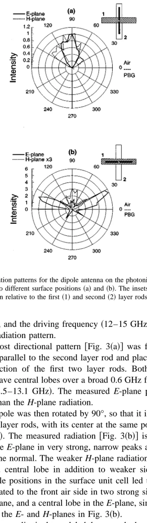
This dipole was then mounted on the stacking surface of our PBG crystal. For driving frequencies within the PBG, we found virtually no radiation propagating through the PBG crystal; as expected the radiation is confined to the air side. However, the angular distribution of the radiated power strongly depended on the driving frequency and the dipole position. Accordingly, we systematically varied the position,
orientation, and the driving frequency ~12–15 GHz! to opti-mize the radiation pattern.
The most directional pattern @Fig. 3~a!# was found for the dipole parallel to the second layer rod and placed above the intersection of the first two layer rods. Both E- and H-planes have central lobes over a broad 0.6 GHz frequency band ~'12.5–13.1 GHz!. The measured E-plane pattern is narrower than the H-plane radiation.
The dipole was then rotated by 90°, so that it is parallel to the first layer rods, with its center at the same position as in Fig. 3~a!. The measured radiation @Fig. 3~b!# is concen-trated in the E-plane in very strong, narrow peaks at'60°– 70° from the normal. The weaker H-plane radiation consists of a broad central lobe in addition to weaker side lobes. Other dipole positions in the surface unit cell led to all the power radiated to the front air side in two strong side peaks in the H-plane, and a central lobe in the E-plane, similar to a reversal of the E- and H-planes in Fig. 3~b!.
We have qualitatively modeled these results by assuming the top two surface layers of the PBG crystal scatter as dis-crete alumina rods, whereas the interior of the crystal be-haves as a highly reflecting bulk. Hence, the radiation pat-terns on the PBG are similar to a dipole placed a distance above a dielectric substrate, accounting for the angular de-pendence of the patterns. Frequency dede-pendence arises since the phase of reflected plane waves from the PBG crystal varies with frequency in the band gap. More detailed
solu-FIG. 2. E- and H-plane radiation patterns for the dipole antenna on a 0.25
in. lexan dielectric sheet~solid! compared with calculations ~dashed!. FIG. 3. Radiation patterns for the dipole antenna on the photonic band gap crystal for two different surface positions~a! and ~b!. The insets shows the dipole position relative to the first~1! and second ~2! layer rods.
tions of EM wave scattering and surface states are needed for a quantitative comparison.
We extracted gains and radiation efficiencies with the standard three-antenna technique and the Friis transmission equations.12The sum of the dipole antenna and horn receiver gains is proportional to the ratio of the peak received power to transmitted power ( Pr/ Pt), and a space factor. The
trans-mitted power was referred to input point c ~Fig. 1! so that dipole, feed cables, phase shifters, and the hybrid coupler were treated as a composite unit with gain Gc. Alternatively,
we subtracted losses from these components~estimated with calibrations to be '25.4 dB!, to extract the input power delivered to the antenna terminals points a and b~Fig. 1! and the gain of the dipole Gab. The directivities are inferred from
radiation pattern measurements, while the corresponding ef-ficiencies (hc,hab) are the ratios of the gain and directivities
~Table I!.
The antenna on the PBG in Fig. 3~a! has a higher gain but a similar efficiency to that on the lexan. The gain and efficiency of the dipole (hc or hab) on the PBG crystal in
Fig. 3~b!, is much larger by a factor of 2, than the lexan, and the efficiency hab exceeded 70%. We also performed mea-surements ~Table I! for ~i! a stycast substrate ~e'12! and found much poorer gains and efficiencies, and~ii! a micros-trip geometry with a metal-back plane behind the duroid and found antenna performance similar to lexan but inferior to the PBG of Fig. 3~b!.
The highly reflecting and dissipation-free PBG crystal, together with the optimized antenna radiation as a function of position on the surface, are promising for applications to high power and directional antennas and antenna arrays. These results are readily scalable to antennas on the higher
frequency millimeter-wave PBG crystals that have the same layer-by-layer structure.
The authors thank R. Weber, W. Leung, M. Sigalas, C. M. Soukoulis, B. Harmon, and E. Brown for helpful discus-sions. This work was supported by the Department of Com-merce through the Center for Advanced Technology~CATD! and the Director for Energy Research, Office of Basic En-ergy Sciences and Advanced EnEn-ergy Projects. The Ames Laboratory is operated for the U. S. Department of Energy by Iowa State University under Contract No. W-7405-Eng-82.
1For a recent review see Photonic Bandgaps and Localization, edited by C. M. Soukoulis~Plenum, New York, 1993!.
2K. M. Ho, C. T. Chan, and C. M. Soukoulis, Phys. Rev. Lett. 65, 3152
~1990!.
3E. Yablonovitch, T. J. Gmitter, and K. M. Leung, Phys. Rev. Lett. 67, 2295
~1991!.
4K. M. Ho, C. T. Chan, C. M. Soukoulis, R. Biswas, and M. Sigalas, Solid State Commun. 89, 413~1994!.
5
E. Ozbay, A. Abeyta, G. Tuttle, M. Tringides, R. Biswas, C. T. Chan, C. M. Soukoulis, and K.-M. Ho, Phys. Rev. B 50, 1945~1994!.
6E. Ozbay, G. Tuttle, R. Biswas, M. Sigalas, and K. M. Ho, Appl. Phys. Lett. 64, 2059~1994!.
7
E. Ozbay, E. Michel, G. Tuttle, R. Biswas, K. M. Ho, J. Bostak, and D. M. Bloom, Opt. Lett. 19, 1155~1994!.
8D. B. Rutledge, D. P. Neikirk, and D. P. Kasilingam, in Infrared and
Millimeter Waves~Academic, Orlando, FL, 1983!, Vol. 10, p. 1, and
ref-erences therein. 9
E. R. Brown, C. D. Parker, and E. J. Yablonovitch, J. Opt. Soc. Am. B 10, 404~1993!.
10E. R. Brown, C. D. Parker, and O. B. McMahon, Appl. Phys. Lett. 64, 3345~1994!.
11
S. D. Cheng, M. S. thesis, Iowa State University, 1995~unpublished!. 12C. A. Balanis, Antenna Theory, Analysis and Design~Harper and Row,
New York, 1982!, p. 716.
TABLE I. The gains and radiation efficiencies for the dipole antenna on different substrates at 13 GHz. These are either referenced~Fig. 1! to point c which includes components, or to the dipole feed points a,b taking out the losses in the system components.
Substrate Position
Directivity D
With coupler Without coupler
Gain Gc Efficiency hc GainGab Efficiency hab Lexan 0.5 in. 1.5 28.4 dB 10% 23.0 dB 33% Stycast 2 in. '1.5 211.8 dB 4% 25.6 dB 18%
Microstrip Metal back '3.0 25.3 dB 10% 0.1 dB 34%
PBG Fig. 3~a! 3.2 24.8 dB 10% 0.6 dB 36%
PBG Fig. 3~b! 3.4 21.4 dB 21% 4.0 dB 74%
3401