A
Reduction in t h e Number of Active
Components used in
Transconductance Grounded Capacitor Filters
Mehmet Ali T a n Bilkent University, P.O. BOX 8, Maltepe, 06572 Ankara
Turkey
Abstract
It is shown that it is possible to reduce the num- ber of transconductance elements in Transconductance Grounded Capacitor filters. This task is achieved via a transformation in LC-ladder prototype and its signal-
flow graph. This reduction saves more active compo- nents in the filters employing differential input trans- conductance elements.
1
Introduction
Monolithic realizations of analog filters have attracted consid- erable interest[1,2,3,6]. One of the recent contributions[l] has suggested two analog filter design schemes using only transcon- ductance elements and grounded capacitors (TGC). The syn- thesis approach is based on signal flow-graphs of passive LC ladder filters. The primary advantage of TGC filters is that all transconductance elements are identical except possibly one. Therefore, semi-custom design is possible by changing only metal-layer mask as can be done in a gate-array design. The other advantage of TGC filters is that they employ only ground- ed capacitors which can be realized on a smaller area than floating ones. Also they are linear with weaker nonideal ef- fects. Against these advantages,one has to weigh the many ac- tive components although the resulting number of transistors are comparable with that of integrated filters using operational amplifiers.
This work proposes a modification in T G C filter synthesis in order to reduce the number of transconductance elements. This modification is based on a transformation in the LC prototype. If there is a capacitor connected between two consecutive pri- mary nodes of the LC ladder prototype, this modification is possible. The approach is similar to what has becn done by G. M. Jacobs et. a1.[4] for the switched-capacitor filters and the work by M. Banu and Y. P. Tsividis[5] for MOSFET-C filters, and the work by F. Krummenacher and
N.
Joehl[G].Rolf S c h a u m a n n Portland State University P.O. Box 751, Portland, Oregon 97207-0751
USA
2
LC-ladder filter, its signal-flow
graph and direct T G C realization
Consider the LC ladder prototype shown in Fig.1.
K S 11
.
v1
vi-'
+Figure 1: LC-ladder prototype
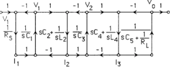
The signal-flow graph corresponding to the primary node volt- ages and the primary mesh currents can be derired[S] as in Fig.2.
1 - 1
v,
1 - 1v2
1 - 1 vo 1~'~~-~~-lII"
4 sL4 s c 5, +- R L1 - 1 1 - 1
11 12 13
Figure 2: Signal-flow graph corresponding to the LC-ladder circuit
The signal-flow graph branches that correspond to the LC res- onance circuits on the horizontal arms of the ladder contain terms which are directly proportional to s. The realization of
this kind of branches results in many transconductances be- cause it can be implemented by considering them as l / ( l / s )
terms. The T G C circuit realizing this signal-flow graph by a direct method is introduced[l] in Fig.3. Note that all gm's are identical (normalized to unity) and all capacitors are grounded. CH2$68-8/9010000-2276$1.00 0 1990 IEEE
Figure 3: TGC circuit realizing the signal-flow graph of Fig.2
3
Transformation in LC-ladder and
its signal flow graph
To reduce the number of active devices, signal-flow graph terms proportional to 3 must be eliminated. This is possible via a
transformation applied to the LC ladder prototype[4,5]. Here, a slightly different approach is chosen as in the following. Coiisider the primary mesh of the LC ladder prototype as shown
i I i Fig.4a and replace the capacitor in the horizontal arm by an
cyuivalent independent current source according to the substi- tution theorem[S] as in Fig.4b. Using the i-shift property[S]
results in the equivalent circuit in Fig.4~.
Figure 4: Equivalent meshes
The signal flow-graph corresponding to the mesh in F i g . 4 ~ is
shown in Fig.5. The overall signal-flow graph corresponding to the LC ladder prototype after using the series of the transfor- mation steps explained above for all such meshes is given in Fig.6.
Figure 5: Signal-flow graph corresponding to the mesh in F i g . 4 ~
Figure 6: Signal-flow graph of the LC prototype after removing the horizont a1 capacitor
4
Synthesis procedure
The final step in this synthesis process is to find the transcon- ductance-C circuit realizing the basic subgraph of the overall signal-flow graph shown in Fig.6. Such a circuit is given in Fig.7 together with its signal-flow graph.
"3
"P
'd
Figure 7: Basic Transconductance-C circuit and its signal-flow graph
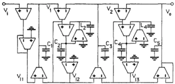
In a way similar to the synthesis procedures based on signal- flow graphs, basic transconductace-C circuits with appropriate element values are tied together to yield the overall signal-flow graph. For the filter in Fig.1 with the graph in Fig.2 as modified in Fig.6, the resulting circuit is shown in Fig.8.
The circuit obtained by this procedure has fewer transconduc- tance elements than the TGC circuit obtained by the direct approch. The transconductances are still identical. The price paid is floating capacitors. Meanwhile, the total capacitance value needed remained intact.
Even better reduction is obtained in the OTA-C version of this circuit. The OTA-C version of the T G C circuit shown in Fig.3 is obtained by combining one inverting and one noninverting transconductance elements with common output nodes into one OTA[9]. The resulting OTA-C filter is shown in Fig.9.
q - E + J - w - c =
1 1 1Figure 8: Transconductance-C circuit with fewer active com- ponents
0
vo
Figure 9: OTA-C circuit realizing the signal-flow graph of Fig.2
The OTA-C circuit with fewer active elements is obtained from the circuit shown in Fig.8 similarly by combining one inverting and one noninverting transconductance with common output node into one OTA The resulting circuit is shown in Fig.10. The number of OTAs is reduced from 13 to 7 while the total capacitance value remains intact.
*
“i
Figure 10: OTA-C circuit with fewer active components
5
Conclusion
A reduction in the number of active components in Transcon- ductance Grounded Capacitor filters is presented. This redud- tion is possible in the case where capacitor loops and/or induc- tor cutsets exist in LC-ladder prototype. A more significant reduction is obtained in the OTA-C version. The number of
OTAs is reduced to 7 from 13 while the total capacitance value remain intact. It is also important to note that all transcon- ductance elements or OTAs are identical except possibly one. The only price paid by this reduction is implementation of some floating capacitors instead of all grounded capacitors.
References
[l] M. A. Tan and R. Schaumann, “Simulating general- parameter LC-ladder filters for for monolithic realizations with only transconductance elements and grounded capac- itors”, IEEE Trans. Circuits and Systems, CAS-36, 299- 307, 1989.
[2] G. W. Roberts and A.
S.
Sedra, “All current-mode fre- quency selective circuits” Electronics Letters, 25, 759-761, 1989.[3] R. Schaumann, “Design of continuous-time fully inte- grated filters: a review” IEE PTOC., 136, Pt. G , 184.190, 1989.
[4] G. M. Jacobs, D. J . Allstot, R. W. Brodersen, and P. R. Gray, “Design techniques for MOS switched capacitor lad- der filters’’ IEEE Trans. Circuits and Ssytems, CAS-25,
1014-1021, 1978.
[5] M. Banu and Y . P. Tsividis, “An elliptic continuous-time CMOS filter with on-chip automatic tuning” IEEE
J.
Solid- Stat e Circuits, SC-20, 11 14- 11 21, 1985.
[6] F . Ibummenacher and
N.
Joehl, “A 4-MHz CMOS continuous-time filter with on-chip automatic tuning” IEEE J . Solid-state Circuits, SC-23, 750-758, 1988. [7] L. A. P. Robichaud, M. Boisvert, and J. Robert, Signal-pow graph.3 and Applications, Englewood Cliffs, NJ, Prentice-Hall, 1961.
[8] L.O. Chua, C. A4. Desoer, and E.
S.
Kuh, Linear and Non- linear Circuits, McGraw-Hill, 1987.[9] M. -4. Tan, “Design and automatic tuning of fully integrated transconductance-grounded capacitor filters”, Ph.D. Thesis, University of Minnesota, USA, 1988.
The procedure described in this work can be applied to the inductors shared by two consecutive meshes by the duality prin- ciple[8].