Journal of Optics
PAPER
Nanosecond pulsed laser ablated sub-10 nm
silicon nanoparticles for improving photovoltaic
conversion efficiency of commercial solar cells
To cite this article: H R Rasouli et al 2017 J. Opt. 19 105902
View the article online for updates and enhancements.
Related content
Enhancement of polycrystalline silicon solar cells efficiency using indium nitride nanoparticles
Sabri Alkis, Farsad Imtiaz Chowdhury, Mustafa Alevli et al.
-Silicon nanoparticles: Preparation, properties, and applications
Chang Huan and Sun Shu-Qing
-Enhancement in c-Si solar cells using 16 nm InN Nanoparticles
Farsad Imtiaz Chowdhury, Aaesha Alnuaimi, Sabri Alkis et al.
Nanosecond pulsed laser ablated sub-10nm
silicon nanoparticles for improving
photovoltaic conversion ef
ficiency of
commercial solar cells
H R Rasouli
1,2, A Ghobadi
2,3, T G Ulusoy Ghobadi
1,2, H Ates
4,
K Topalli
1,2and A K Okyay
1,2,31
Institute of Materials Science and Nanotechnology, Bilkent University, 06800 Ankara, Turkey
2UNAM—National Nanotechnology Research Center, Bilkent University, Bilkent, Ankara 06800, Turkey 3
Department of Electrical and Electronics Engineering, Bilkent University, 06800 Ankara, Turkey
4
Department of Metallurgical and Materials Engineering, The Faculty of Technology, Gazi University, 06500, Ankara, Turkey
E-mail:[email protected]
Received 25 January 2017, revised 7 July 2017 Accepted for publication 8 August 2017 Published 11 September 2017
Abstract
In this paper, we demonstrate the enhancement of photovoltaic(PV) solar cell efficiency using luminescent silicon nanoparticles(Si-NPs). Sub-10 nm Si-NPs are synthesized via pulsed laser ablation technique. These ultra-small Si nanoparticles exhibit photoluminescence(PL) character tics at 425 and 517 nm upon excitation by ultra-violet(UV) light. Therefore, they can act as secondary light sources that convert high energetic photons to ones at visible range. This down-shifting property can be a promising approach to enhance PV performance of the solar cell, regardless of its type. As proof-of-concept, polycrystalline commercial solar cells with an efficiency of ca 10% are coated with these luminescent Si-NPs. The nanoparticle-decorated solar cells exhibit up to 1.64% increase in the external quantum efficiency with respect to the uncoated reference cells. According to spectral photo-responsivity characterizations, the efficiency enhancement is stronger in wavelengths below 550 nm. As expected, this is attributed to down-shifting via Si-NPs, which is verified by their PL characteristics. The results presented here can serve as a beacon for future performance enhanced devices in a wide range of applications based on Si-NPs including PVs and LED applications.
Keywords: silicon nanoparticle, laser ablation, solar cell, efficiency enhancement (Some figures may appear in colour only in the online journal)
1. Introduction
Silicon nanoparticles (Si-NPs) are promising candidates for various applications ranging from optoelectronics to bioen-gineering. The attention toward ultra-small Si-NPs is sky-rocketing due to the fascinating optical and electrical properties, distinctive photoluminescence(PL) and favorable nontoxicity and biocompatibility. Therefore, the use of Si-NPs in various technologies and applications such as light emitting diodes[1,2], photovoltaics (PVs) [3,4], lithium ion
batteries[5,6], catalysts [7,8], fluorescence imaging [9,10], and memories[11–14] is rapidly increasing.
There are various alternative methods for Si-NPs synthesis including pulsed laser ablation[15], chemical vapor deposition [16], ion implantation [17], electrochemical etching [18], thermal decomposition of silane [19], ball milling [20] and plasma synthesis [21]. However, high volume of ultra-small Si-NPs production is one of the most challenging issues. Among these methods, pulsed laser ablation in liquid(PLAL) is a high-throughput approach for synthesis of ultra-small J. Opt. 19(2017) 105902 (6pp) https://doi.org/10.1088/2040-8986/aa84dd
Si-NPs. It is a clean, simple and versatile method resulting in highly-pure and stable NPs[22]. The main advantages of this method are that NPs are stable without adding stabilizing surfactants and can avoid potential drawbacks of using che-mical products and multi-step procedures for the NPs size control [23]. Control of experimental conditions and applic-ability to a wide range of materials make PLAL method a preferred technique for researchers. The products rely upon laser parameters such as pulse time duration, wavelength, repetition rate and scan pattern as well as liquid properties [24, 25]. PLAL Si-NP synthesis in various media has been widely investigated by nanosecond[26,27] and femtosecond [28] pulse laser duration.
Solid state light emission utilizing silicon as the semi-conductor medium is a rapidly growing area of research in addition to the search toward monolithic light sources that can be used on the chip-scale [29–32]. Silicon is an indirect bandgap semiconductor that exhibits remarkable optical and electronic variation when its size becomes comparable to the bulk exciton Bohr radius (4 nm for silicon) [33]. In these ranges, band-to-band radiative recombination dominants are compared to phonon-assisted indirect band-gap transitions, resulting in enhanced PL intensity [34]. It is confirmed that bright PL from low-dimensional silicon is primarily located in visible red regions (maximum about 700 nm) [35]. Such phenomena has been employed in quite a few technologies, such as luminescent imaging probes forfluorescence imaging [36] and light emitting diode integrated with luminescent silicon to generate multiple colors using single material[37]. PV technologies are becoming increasingly common as a renewable energy alternative. The silicon PV technology has been improved over decades, however, even a small increase in the PV cell efficiency can make a huge overall impact on energy savings due to the sheer size of the installed PV capacity. One approach that researchers take is to circumvent the spectral mismatch between the energy distribution of incident photons and the bandgap of silicon [38]. In this regard, luminescent materials have been offered as a solution by converting a broad spectrum of light into photons of a particular wavelength and minimizing the losses in the solar-cell-based energy conversion process. One such approach for solar cell efficiency enhancement is down-shifting materials which absorb the short-wavelength light (300–500 nm) and re-emitting them at a longer wavelength where the external quantum efficiency of the PV device is higher. Alkis et al [39,40] presents enhancement in power performance of an indium nitride particle/polycrystalline silicon solar cell and attributes it to the down-shifting properties of the InN particles. Stupca et al [41] investigates the effect of mono-dispersed luminescent Si nanoparticles coating on poly-crystalline silicon solar cell and explains the device enhancement by wavelength down conversion. Svrcek et al [42] reports IQE enhancement in the region where the Si nanocrystals PL excitation occurs and refers it to a boost on carrier collections via the luminescence converter.
In this work, we demonstrate beneficial effect of ultra-small luminescent Si-NPs synthesized via laser ablation on efficiency enhancement of a commercial silicon solar cell. In
the following, Si-NPs synthesis is presented followed by materials and solar cell characterizations.
2. Experimental details
A 500μm thick p-type (100) silicon wafer with a resistivity of 0.1Ω cm was cleaned by sonification in acetone prior to laser ablation without any further purification. The cleaned Si wafer was placed in a glass vessel containing 5 ml of pure deionized water. The laser ablation was carried out by the OKYAYTECH Laser Nanoparticle Synthesis System that utilizes a fiber laser (NUQA, 1064 nm wavelength, 30 Hz repetition rate, 100 ns pulse duration). The laser beam is scanned spirally over the target surface for ∼15 min that yielded a light-orange solution. The choice of spiral scanning shape is discussed elsewhere[43]. The laser fluence is chosen to be 6 mJ pulse−1 and scan speed is fixed at 2000 mm s−1. Then the target Si wafer is removed and ablation is applied on solution for 3 h to obtain blue luminescent Si solution [43].
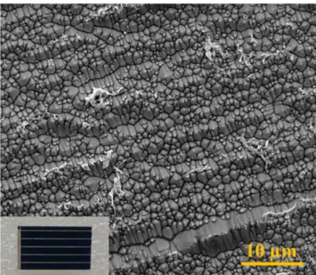
High resolution transmission electron microscopy(TEM) images of Si-NPs were obtained using an FEI-Technai G2F30 type instrument at an operating voltage of 300 kV. TEM samples were prepared by drop-casting the solution on car-bon-coated TEM grids. The optical absorption spectrum of the Si-NPs is measured using Varian Cary 5000 UV/Vis/ NIR spectrometer and PL spectrum is obtained using a Varian spectrofluorometer. The commercial solar cell was purchased from the Delsolar company, People’s Republic of China. Figure 1 shows the scanning electron microscopy image of solar cell texture where the overall view of the cell is shown in the inset. The cell is cut into smaller pieces with the area of 1.5 cm×1 cm in a way that all electrical grid lines are connected and cover the whole sample active area.
Si-NPs were spin coated on top of the cell multiple times at a spin speed of 1200 rpm for 30 s in each cycle. Current–voltage Figure 1.Surface morphology of the commercial solar cell obtained by scanning electron microscope(SEM) image. Inset: photograph of the cell, Delsolar D6E.
2
characteristics and spectral response are studied before and after NPs coatings on the solar cell. The J–V curve testing system of PV measurement(Newport solar simulator Model 67005) was used for current–voltage characteristics. The input power of the solar simulator lamp is 100 mW Cm−2. In order to measure photoresponsivity for the wavelengths between 400 and 800 nm, we used a Xenon-lamp illuminator. The output of the lamp goes through an Oriel 74004 monochromator(1/8 m, 1200 lines/mm grating). The monochromatic light is collimated and chopped with a mechanical chopper at a chop speed of 380 Hz, which is also read by a lock-in amplifier (SR830). The short circuit cur-rent was measured by the lock-in amplifier. Also, a calibrated Si detector was used at the sample position to collect the light source power at each wavelength step.
3. Results and discussion
TEM results depicted in figure2 confirm the generation of sub-10 nm Si-NPs through laser ablation. Spherical-like nanoparticles with the average size of 8 nm without any aggregation can be observed. The histogram of Si nano-particle sizes counted from TEM images predicts that the particle sizes range from 6 to 14 nm.
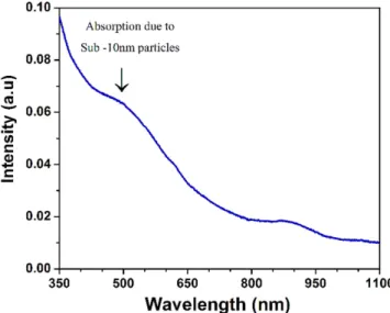
Figure3 shows the UV–vis absorption spectrum of the synthesized Si-NPs. All absorption spectra appear to have a broad continuous band between 350 and 1100 nm and a distinctive shoulder with a minimum absorbance at around 400 nm. The absorption peak at 490 nm is attributed to Si NPs with sub-10 nm size, which is in agreement with other research works on Si-NPs[44,45].
The PL spectrum of Si-NPs at an excitation wavelength of 310 nm is given in figure4. According to the
quantum-confinement theory for nanoscale silicon structures, the broad PL spectrum is attributed to the presence of a wide distribu-tion of nanocrystal sizes [46]. The PL spectra exhibit rather large peaks centered at approximately 425 and 517 nm. The peak at 425 nm shows blue light emission of Si-NPs solution corresponding to sub-10 nm particles [47]. Quantum con-finement of excitons in nanometer scale is the principal mechanism for high PL of low dimensional silicon particles [48]. However, surface states and defects can effectively increase the PL intensity. During the ablation, generated Si-NPs are in contact with water therefore surrounded with SiO2. It is confirmed that the defects in SiO2of oxidized Si-NPs efficiently luminesce in blue region [49, 50]. The red-shifted emission at 517 nm can be attributed to larger size dispersion varying from 10 to 120 nm. Accordingly, there are Figure 2.Transmission electron microscopy(TEM) images of laser synthesized Si-NPs with size distribution given in the inset.
some particles, the size of which are larger than Bohr radius leading to weak confinement regime and higher wavelength luminescent. Therefore, a red-shifted emission with lower energy band gap is observed[51].
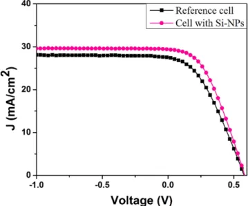
Figure5 shows the J–V characteristics of the reference solar cell and the Si-NPs deposited cell with the bias voltage swept from 0 to 1 V. There is a sharp increase in current density values for bias voltages lower than 0 V. The current density is almost constant within 0 to −1 V bias voltage, which indicates efficient collection of charge carriers and the eventual saturation of the carrier drift velocity[52]. Table1 summarizes the results of the solar cell parameters(Voc, Jsc, fill factors, and efficiencies). As seen from the table, 1.94 mA cm−2increase in Jscvalue leads to a 1.64% increase in the overall absolute cell efficiency of Si-NPs; decorated cell with respect to the reference.
Figure 6 shows the photo-current response spectrum of the reference and Si-NPs decorated cell. The photocurrent spectroscopy of Si-NPs-decorated cell shows a significant increase at high photon energy excitations(300–600 nm) with respect to the reference cell. Such an enhancement can be attributed to PL emission of nanoparticles in which incident high energy photons are converted to visible lower energy photons that is absorbed by the silicon cell[53]. Accordingly, thermalisation losses can be reduced by using down-conver-sion whereby non-radiative losses can be prevented. This leads to an increase in the carrier collection probability in the region where the conversion appears. The photo-current response curves of Si-NPs decorated cell and reference cell converge together in longer excitation wavelength (>∼600 nm) verifying the absence of NPs scattering as an enhancement mechanism. It should also be noted that, in addition to sub-10 nm silicon particles, we have synthesized larger Si-NPs from 50 to 400 nm by laser ablation and carried out similar experiments by decorating pristine reference cells. There was no significant enhancement observed by applying Si-NPs range from 50 to 400 nm, indicating that luminescence of Si-NPs is the primary source to achieve efficiency enhancement.
4. Conclusion
This work shows that laser ablated luminescent Si-NPs have a constructive effect on the PV device efficiency. The solar cells decorated with sub-10 nm particles synthesized in deionized water show absolute increase in solar cell efficiency up to 1.64% compared to a reference solar cell without any Si NPs on it. The enhancement is attributed to the wavelength down shifting generated by luminescent Si-NPs, confirmed by spectral photo-current responsivity enhancement below 550 nm. The results show the ability of pulsed laser ablation method as a viable solution to produce sub-10 nm Si-NPs applicable for third generation solar cells. Pulse laser ablation Figure 4.PL spectrum of Si-NPs at an excitation wavelength of
310 nm.
Figure 5.The J–V curves of the NP decorated and reference solar cells.
Figure 6.Spectral photoresponsivity of the NP decorated and reference solar cells under 0.6 V reverse bias.
4
in liquids can offer a direct cost-effective approach for non-toxic luminescent colloidal Si-NPs synthesis applicable to further demands in various technologies.
Funding
This work was partially supported by the Scientific and Technological Research Council of Turkey (TUBITAK) under Grant Nos. 112M004, 112E052, and 113M815. AKO acknowledges support from the Turkish Academy of Sciences
Distinguished Young Scientist Award (TUBA GEBIP),
BAGEP Award and FABED Award.
References
[1] Maier-Flaig F, Rinck J, Stephan M, Bocksrocker T, Bruns M, Kübel C, Powell A K, Ozin G A and Lemmer U 2013 Multicolor silicon light-emitting diodes(SiLEDs) Nano Lett. 13475–80
[2] Puzzo D P, Henderson E J, Helander M G, Wang Z, Ozin G A and Lu Z 2011 Visible colloidal nanocrystal silicon light-emitting diode Nano Lett.111585–90 [3] Cho E-C, Park S, Hao X, Song D, Conibeer G, Park S-C and
Green M A 2008 Silicon quantum dot/crystalline silicon solar cells Nanotechnology19245201
[4] Conibeer G, Green M, Cho E-C, König D, Cho Y-H, Fangsuwannarak T, Scardera G, Pink E, Huang Y and Puzzer T 2008 Silicon quantum dot nanostructures for tandem photovoltaic cells Thin Solid Films5166748–56 [5] Ge M, Rong J, Fang X and Zhou C 2012 Porous doped silicon
nanowires for lithium ion battery anode with long cycle life Nano Lett.122318–23
[6] Zhu B, Jin Y, Tan Y, Zong L, Hu Y, Chen L, Chen Y, Zhang Q and Zhu J 2015 Scalable production of Si nanoparticles directly from low grade sources for lithium-ion battery anode Nano Lett.155750–4
[7] Peng F, Wang J, Ge G, He T, Cao L, He Y, Ma H and Sun S 2013 Photochemical reduction of CO2catalyzed by silicon
nanocrystals produced by high energy ball milling Mater. Lett.9265–7
[8] Kang Z, Tsang C H A, Wong N-B, Zhang Z and Lee S-T 2007 Silicon quantum dots: a general photocatalyst for reduction, decomposition, and selective oxidation reactions J. Am. Chem. Soc.12912090–1
[9] Erogbogbo F, Yong K-T, Roy I, Hu R, Law W-C, Zhao W, Ding H, Wu F, Kumar R and Swihart M T 2010 In vivo targeted cancer imaging, sentinel lymph node mapping and multi-channel imaging with biocompatible silicon
nanocrystals ACS Nano5413–23
[10] Gu L, Hall D J, Qin Z, Anglin E, Joo J, Mooney D J, Howell S B and Sailor M J 2013 In vivo time-gated fluorescence imaging with biodegradable luminescent porous silicon nanoparticles Nat. Commun.42326 [11] El‐Atab N, Ozcan A, Alkis S, Okyay A K and Nayfeh A 2014
Silicon nanoparticle charge trapping memory cell Phys. Status Solidi8629–33
[12] El-Atab N, Ozcan A, Alkis S, Okyay A K and Nayfeh A 2014 Low power zinc-oxide based charge trapping memory with embedded silicon nanoparticles via poole-frenkel hole emission Appl. Phys. Lett.104013112
[13] El-Atab N, Turgut B B, Okyay A K, Nayfeh M and Nayfeh A 2015 Enhanced non-volatile memory characteristics with quattro-layer graphene nanoplatelets versus 2.85 nm Si nanoparticles with asymmetric Al2O3/HfO2tunnel oxide
Nanoscale Res. Lett.101–7
[14] El‐Atab N, Rizk A, Tekcan B, Alkis S, Okyay A K and Nayfeh A 2016 Memory effect by charging of ultra‐small 2 nm laser‐synthesized solution processable Si‐nanoparticles embedded in Si–Al2O3–SiO2structure[Phys. Status Solidi
A 212, 1751–1755 (2015)] Phys. Status Solidi a2132264 [15] Alkis S, Okyay A K and Ortaç B 2012 Post-treatment of silicon
nanocrystals produced by ultra-short pulsed laser ablation in liquid: toward blue luminescent nanocrystal generation J. Phys. Chem. C1163432–6
[16] Cheng Q, Xu S and Ostrikov K K 2010 Single-step, rapid low-temperature synthesis of Si quantum dots embedded in an amorphous SiC matrix in high-density reactive plasmas Acta Mater.58560–9
[17] Dumas C, Grisolia J, Ressier L, Arbouet A, Paillard V, Ben Assayag G, Claverie A, Van den Boogaart M and Brugger J 2007 Synthesis of localized 2D‐layers of silicon nanoparticles embedded in a SiO2layer by a stencil‐masked
ultra‐low energy ion implantation process Phys. Status Solidi a204487–91
[18] Clark H R Jr and Ahern B S 1997 Method for producing semiconductor particles US Patent Specification US5690807
[19] Mangolini L, Thimsen E and Kortshagen U 2005 High-yield plasma synthesis of luminescent silicon nanocrystals Nano Lett.5655–9
[20] Kuang L, Mitchell B S and Fink M J 2015 Silicon
nanoparticles synthesised through reactive high-energy ball milling: enhancement of optical properties from the removal of iron impurities J. Exp. Nanosci.101214–22
[21] Kramer N, Anthony R, Mamunuru M, Aydil E and
Kortshagen U 2014 Plasma-induced crystallization of silicon nanoparticles J. Phys. D: Appl. Phys.47075202
[22] Intartaglia R, Bagga K and Brandi F 2014 Study on the productivity of silicon nanoparticles by picosecond laser ablation in water: towards gram per hour yield Opt. Express 223117–27
[23] Semaltianos N 2016 Nanoparticles by laser ablation of bulk target materials in liquids Handbook of Nanoparticles (Thessaloniki: Springer)pp 67–92
[24] Sasaki K and Takada N 2010 Liquid-phase laser ablation Pure Appl. Chem.821317–27
[25] Brandi F 2015 Nanoparticle generation by pulsed laser ablation in liquid 20th Symp. on Application of Plasma Processes p 22
[26] Abderrafi K, García Calzada R L, Gongalsky M B, Suárez I, Abarques R, Chirvony V S, Timoshenko V Y, Ibánez R and Martínez-Pastor J P 2011 Silicon nanocrystals produced by nanosecond laser ablation in an organic liquid J. Phys. Chem. C1155147–51
[27] Popovic D, Chai J, Zekic A, Trtica M, Momcilovic M and Maletic S 2012 Synthesis of silicon-based nanoparticles by Table 1.Solar cell efficiency parameters.
Voc(V) Jsc(mA cm−2) Efficiency (%) Fill factor
Reference solar cell 0.58 27.48 9.01 56.56
10.6μm nanosecond CO2laser ablation in liquid Laser
Phys. Lett.10026001
[28] Kuzmin P G, Shafeev G A, Bukin V V, Garnov S V, Farcau C, Carles R, Warot-Fontrose B, Guieu V and Viau G 2010 Silicon nanoparticles produced by femtosecond laser ablation in ethanol: size control, structural characterization, and optical properties J. Phys. Chem. C11415266–73 [29] Okyay A K, Kuzum D, Latif S, Miller D A and Saraswat K C
2007 Silicon germanium CMOS optoelectronic switching device: bringing light to latch IEEE Trans. Electron. Devices 543252–9
[30] Okyay A K, Pethe A J, Kuzum D, Latif S, Miller D A and Saraswat K C 2007 SiGe optoelectronic metal-oxide semiconductorfield-effect transistor Opt. Lett.322022–4 [31] Yu H-Y, Cheng S.-l., Park J-H, Okyay A K, Onbaşlı M C,
Ercan B, Nishi Y and Saraswat K C 2010 High quality single-crystal germanium-on-insulator on bulk Si substrates based on multistep lateral over-growth with hydrogen annealing Appl. Phys. Lett.97063503
[32] Onaran E, Onbasli M C, Yesilyurt A, Yu H Y,
Nayfeh A M and Okyay A K 2012 Silicon-Germanium multi-quantum well photodetectors in the near infrared Opt. Express207608–15
[33] Yurtsever A, Weyland M and Muller D A 2006 Three-dimensional imaging of nonspherical silicon nanoparticles embedded in silicon oxide by plasmon tomography Appl. Phys. Lett.89151920
[34] Huan C and Shu-Qing S 2014 Silicon nanoparticles: preparation, properties, and applications Chin. Phys. B23 088102
[35] Pavesi L, Dal Negro L, Mazzoleni C, Franzo G and Priolo F 2000 Optical gain in silicon nanocrystals Nature408 440–4
[36] Joo J, Liu X, Kotamraju V R, Ruoslahti E, Nam Y and Sailor M J 2015 Gated luminescence imaging of silicon nanoparticles ACS Nano96233–41
[37] Li X, He Y, Talukdar S S and Swihart M T 2003 Process for preparing macroscopic quantities of brightly
photoluminescent silicon nanoparticles with emission spanning the visible spectrum Langmuir198490–6 [38] Huang X, Han S, Huang W and Liu X 2013 Enhancing solar
cell efficiency: the search for luminescent materials as spectral converters Chem. Soc. Rev.42173–201 [39] Alkis S, Chowdhury F I, Alevli M, Dietz N, Yalızay B,
Aktürk S, Nayfeh A and Okyay A K 2015 Enhancement of polycrystalline silicon solar cells efficiency using indium nitride particles J. Opt.17105903
[40] Chowdhury F I, Islam K, Alkis S, Ortaç B, Alevli M, Dietz N, Okyay A and Nayfeh A 2015 Enhanced light scattering with energy downshifting using 16 nm indium nitride
nanoparticles for improved thin-film a-Si NIP solar cells ECS Trans.669–16
[41] Stupca M, Alsalhi M, Al Saud T, Almuhanna A and Nayfeh M 2007 Enhancement of polycrystalline silicon solar cells using ultrathinfilms of silicon nanoparticle Appl. Phys. Lett. 91063107
[42] Švrček V, Slaoui A and Muller J-C 2004 Silicon nanocrystals as light converter for solar cells Thin Solid Films451384–8 [43] Ulusoy Ghobadi A G T G, Okyay T, Topalli K and Okyay A K 2016 Controlling luminescent silicon nanoparticles emission produced by nanosecond pulsed laser ablation: role of interface defect states and crystallinity phase RSC Adv.6 112520–6
[44] Intartaglia R, Bagga K, Brandi F, Das G, Genovese A, Di Fabrizio E and Diaspro A 2011 Optical properties of femtosecond laser-synthesized silicon nanoparticles in deionized water J. Phys. Chem. C1155102–7 [45] Rosso-Vasic M, Spruijt E, Popović Z, Overgaag K,
Van Lagen B, Grandidier B, Vanmaekelbergh D, Domínguez-Gutiérrez D, De Cola L and Zuilhof H 2009 Amine-terminated silicon nanoparticles: synthesis, optical properties and their use in bioimaging J. Mater. Chem.19 5926–33
[46] Hybertsen M S 1994 Absorption and emission of light in nanoscale silicon structures Phys. Rev. Lett.721514 [47] Belomoin G, Therrien J, Smith A, Rao S, Twesten R, Chaieb S,
Nayfeh M, Wagner L and Mitas L 2002 Observation of a magic discrete family of ultrabright Si nanoparticles Appl. Phys. Lett.80841–3
[48] Bisi O, Ossicini S and Pavesi L 2000 Porous silicon: a quantum sponge structure for silicon based optoelectronics Surf. Sci. Rep.381–126
[49] Wolkin M, Jorne J, Fauchet P, Allan G and Delerue C 1999 Electronic states and luminescence in porous silicon quantum dots: the role of oxygen Phys. Rev. Lett.82197 [50] Švrček V, Sasaki T, Shimizu Y and Koshizaki N 2006 Blue luminescent silicon nanocrystals prepared by ns pulsed laser ablation in water Appl. Phys. Lett.89213113
[51] Intartaglia R, Bagga K, Scotto M, Diaspro A and Brandi F 2012 Luminescent silicon nanoparticles prepared by ultra short pulsed laser ablation in liquid for imaging applications Opt. Mater. Express2510–8
[52] Alkis S, Tekcan B, Nayfeh A and Okyay A K 2013 UV/vis range photodetectors based on thinfilm ALD grown ZnO/Si heterojunction diodes J. Opt.15105002
[53] Strümpel C, McCann M, Beaucarne G, Arkhipov V, Slaoui A, Švrček V, Del Cañizo C and Tobias I 2007 Modifying the solar spectrum to enhance silicon solar cell efficiency—an overview of available materials Sol. Energy Mater. Sol. Cells91238–49
6