Photonic band gaps with layerbylayer doubleetched structures
R. Biswas, E. Özbay, and K.M. Ho
Citation: J. Appl. Phys. 80, 6749 (1996); doi: 10.1063/1.363802 View online: http://dx.doi.org/10.1063/1.363802
View Table of Contents: http://jap.aip.org/resource/1/JAPIAU/v80/i12
Published by the American Institute of Physics.
Additional information on J. Appl. Phys.
Journal Homepage: http://jap.aip.org/
Journal Information: http://jap.aip.org/about/about_the_journal
Top downloads: http://jap.aip.org/features/most_downloaded
Photonic band gaps with layer-by-layer double-etched structures
R. Biswasa)Microelectronics Research Center, Ames Laboratory–USDOE and Department of Physics and Astronomy, Iowa State University, Ames, Iowa 50011
E. O¨ zbay
Department of Physics, Bilkent University, Bilkent, Ankara 06533, Turkey
K.-M. Ho
Microelectronics Research Center, Ames Laboratory–USDOE and Department of Physics and Astronomy, Iowa State University, Ames, Iowa 50011
~Received 25 July 1996; accepted for publication 3 September 1996!
Periodic layer-by-layer dielectric structures with full three-dimensional photonic band gaps have been designed and fabricated. In contrast to previous layer-by-layer structures the rods in each successive layer are at an angle of 70.5° to each other, achieved by etching both sides of a silicon wafer. Photonic band-structure calculations are utilized to optimize the photonic band gap by varying the structural geometry. The structure has been fabricated by double etching Si wafers producing millimeter wave photonic band gaps between 300 and 500 GHz, in excellent agreement with band calculations. Overetching this structure produces a multiply connected geometry and increases both the size and frequency of the photonic band gap, in very good agreement with experimental measurements. This new robust double-etched structure doubles the frequency possible from a single Si wafer, and can be scaled to produced band gaps at higher frequencies. © 1996 American Institute of Physics.@S0021-8979~96!01224-8#
INTRODUCTION
In analogy with the electronic energy bands in a crystal, electromagnetic waves propagating in a periodic dielectric structure are organized into photonic bands, which may be separated by a gap or frequency region where the propaga-tion of the electromagnetic waves is forbidden.1 Several analogies exist between the electronic Bloch states and elec-tromagnetic wave propagation. Theoretical calculations of Ho, Chan, and Soukoulis2predicted that the diamond struc-ture possesses a full three-dimensional photonic band gap. An experimental ‘‘three-hole’’ structure with the symmetry of the diamond structure was fabricated by Yablonovitch, Gmitter, and Leung3 at microwave length scales that had a full three-dimensional photonic band gap~PBG!. This three-hole structure was an important proof-of-concept demonstra-tion of photonic band gaps. An important direcdemonstra-tion in ongo-ing work has been to design and fabricate PBG structures at smaller length scales, directed toward optical and infrared frequencies.
Recently the Iowa State group designed4 a new dimensional layer-by-layer structure with a full three-dimensional photonic band gap. The gap exists over a wide range of structural parameters. This structure was first fabricated5 in the microwave regime by stacking alumina cylinders and demonstrated to have a full three-dimensional PBG at microwave frequencies~12–14 GHz!, with measure-ments in very good agreement with the theoretically pre-dicted photonic band structure. The simplicity of this layer-by-layer structure then led to the fabrication6of this structure at progressively smaller length scales using micromachined silicon wafers and conventional semiconductor processing
techniques. The micromachining technique first led to Si wa-fers with photonic midgap band-gap frequencies of 100 GHz,6 followed by fabrication of a smaller-scale structure with midgap frequencies at 450 GHz.7This structure has the promise of being extended to higher frequencies in the infra-red regime.
Concurrently there is a need8 to design new structures with three-dimensional photonic bandgaps that
~i! that can produce higher-frequency bandgaps,
~ii! are robust, and
~iii! have advantages for fabrication that would make such a structure more suitable for applications in the mi-crowave and millimeter wave regime.
Such a structure is proposed and discussed here. Al-though experimental fabrication and limited measurements of the transmission through the structure have been presented separately,9 the analysis of the structural geometry, optimi-zation of the structure for improving the PBG, and the pho-tonic band calculations have not been discussed previously.
PHOTONIC BAND-GAP STRUCTURE
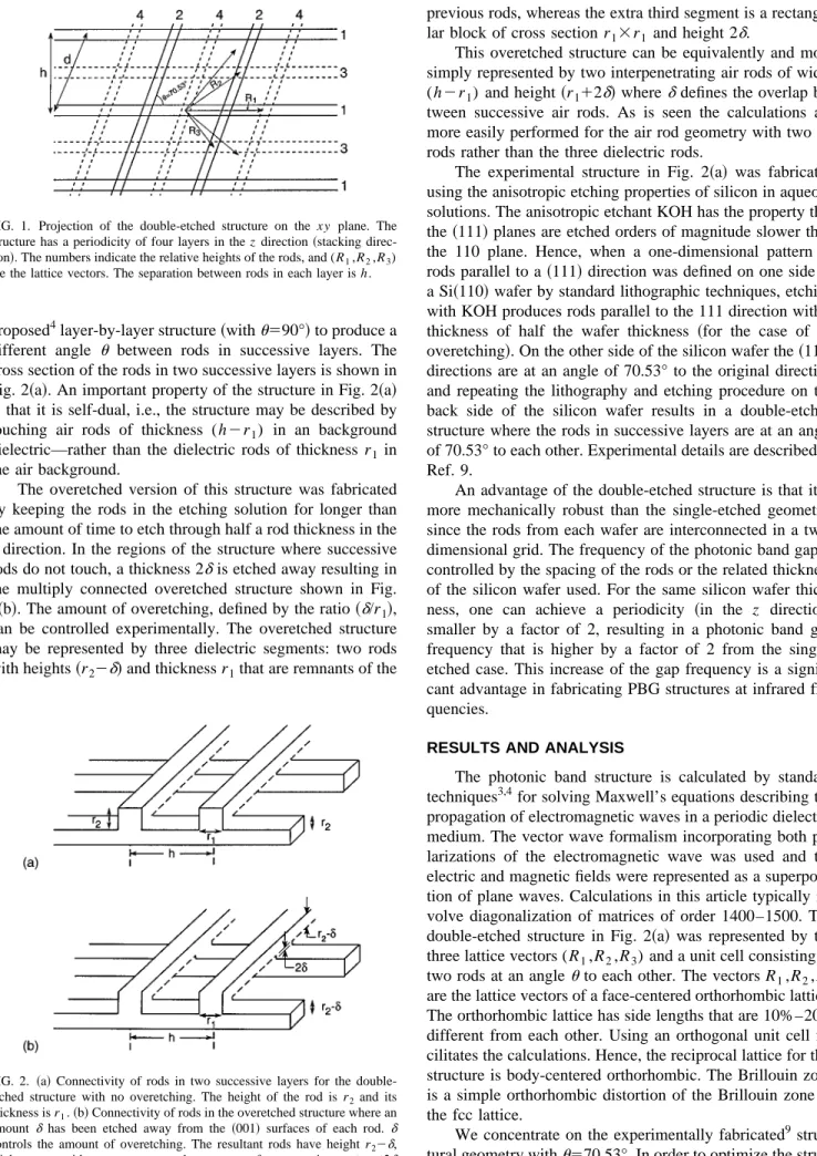
The three-dimensional PBG structure is a layer-by-layer structure that was designed and fabricated in this paper and is shown in Fig. 1. Each layer consists of a set of parallel di-electric rods with centers separated by h. The rods in the next layer are rotated by an angle u with respect to rods in the previous layer. u has values different from 90°, and is 70.53° and in general can vary from 90° to 60° but still have a full three-dimensional PBG. The rods in the second neigh-bor plane are shifted by half the spacing h relative to rods in the first plane. The structure has a periodicity of four layers in the z direction and is obtained by shearing the originally
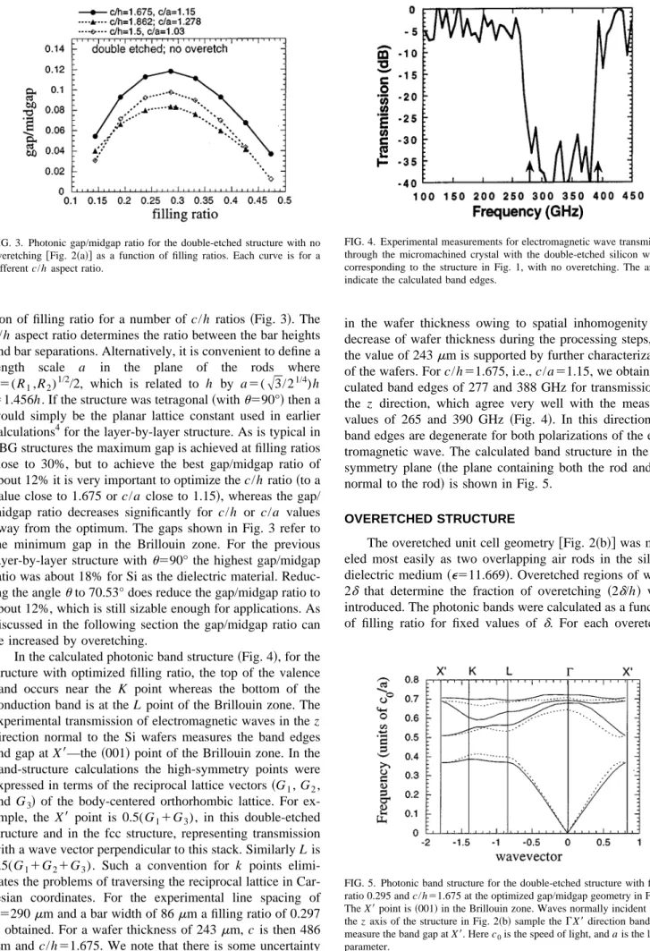
proposed4layer-by-layer structure~withu590°! to produce a different angle u between rods in successive layers. The cross section of the rods in two successive layers is shown in Fig. 2~a!. An important property of the structure in Fig. 2~a! is that it is self-dual, i.e., the structure may be described by touching air rods of thickness (h2r1) in an background
dielectric—rather than the dielectric rods of thickness r1 in
the air background.
The overetched version of this structure was fabricated by keeping the rods in the etching solution for longer than the amount of time to etch through half a rod thickness in the
z direction. In the regions of the structure where successive
rods do not touch, a thickness 2dis etched away resulting in the multiply connected overetched structure shown in Fig. 2~b!. The amount of overetching, defined by the ratio ~d/r1!,
can be controlled experimentally. The overetched structure may be represented by three dielectric segments: two rods with heights~r22d! and thickness r1that are remnants of the
previous rods, whereas the extra third segment is a rectangu-lar block of cross section r13r1 and height 2d.
This overetched structure can be equivalently and more simply represented by two interpenetrating air rods of width (h2r1) and height~r112d! whered defines the overlap be-tween successive air rods. As is seen the calculations are more easily performed for the air rod geometry with two air rods rather than the three dielectric rods.
The experimental structure in Fig. 2~a! was fabricated using the anisotropic etching properties of silicon in aqueous solutions. The anisotropic etchant KOH has the property that the ~111! planes are etched orders of magnitude slower than the 110 plane. Hence, when a one-dimensional pattern of rods parallel to a ~111! direction was defined on one side of a Si~110! wafer by standard lithographic techniques, etching with KOH produces rods parallel to the 111 direction with a thickness of half the wafer thickness ~for the case of no overetching!. On the other side of the silicon wafer the ~111! directions are at an angle of 70.53° to the original direction and repeating the lithography and etching procedure on the back side of the silicon wafer results in a double-etched structure where the rods in successive layers are at an angle of 70.53° to each other. Experimental details are described in Ref. 9.
An advantage of the double-etched structure is that it is more mechanically robust than the single-etched geometry, since the rods from each wafer are interconnected in a two-dimensional grid. The frequency of the photonic band gap is controlled by the spacing of the rods or the related thickness of the silicon wafer used. For the same silicon wafer thick-ness, one can achieve a periodicity ~in the z direction! smaller by a factor of 2, resulting in a photonic band gap frequency that is higher by a factor of 2 from the single-etched case. This increase of the gap frequency is a signifi-cant advantage in fabricating PBG structures at infrared fre-quencies.
RESULTS AND ANALYSIS
The photonic band structure is calculated by standard techniques3,4for solving Maxwell’s equations describing the propagation of electromagnetic waves in a periodic dielectric medium. The vector wave formalism incorporating both po-larizations of the electromagnetic wave was used and the electric and magnetic fields were represented as a superposi-tion of plane waves. Calculasuperposi-tions in this article typically in-volve diagonalization of matrices of order 1400–1500. The double-etched structure in Fig. 2~a! was represented by the three lattice vectors (R1,R2,R3) and a unit cell consisting of two rods at an angleuto each other. The vectors R1,R2,R3
are the lattice vectors of a face-centered orthorhombic lattice. The orthorhombic lattice has side lengths that are 10%–20% different from each other. Using an orthogonal unit cell fa-cilitates the calculations. Hence, the reciprocal lattice for this structure is body-centered orthorhombic. The Brillouin zone is a simple orthorhombic distortion of the Brillouin zone of the fcc lattice.
We concentrate on the experimentally fabricated9 struc-tural geometry withu570.53°. In order to optimize the struc-ture, the gap/midgap frequency ratio is calculated as a
func-FIG. 1. Projection of the double-etched structure on the xy plane. The structure has a periodicity of four layers in the z direction~stacking direc-tion!. The numbers indicate the relative heights of the rods, and (R1,R2,R3)
are the lattice vectors. The separation between rods in each layer is h.
FIG. 2. ~a! Connectivity of rods in two successive layers for the double-etched structure with no overetching. The height of the rod is r2and its
thickness is r1.~b! Connectivity of rods in the overetched structure where an
amount dhas been etched away from the ~001! surfaces of each rod. d controls the amount of overetching. The resultant rods have height r22d,
thickness r1, with an extra rectangular segment of cross section r13r132d
connecting the rods.
tion of filling ratio for a number of c/h ratios ~Fig. 3!. The
c/h aspect ratio determines the ratio between the bar heights
and bar separations. Alternatively, it is convenient to define a
length scale a in the plane of the rods where
a5(R1,R2)1/2/2, which is related to h by a5(
A
3/21/4)h51.456h. If the structure was tetragonal ~withu590°! then a
would simply be the planar lattice constant used in earlier calculations4for the layer-by-layer structure. As is typical in PBG structures the maximum gap is achieved at filling ratios close to 30%, but to achieve the best gap/midgap ratio of about 12% it is very important to optimize the c/h ratio~to a value close to 1.675 or c/a close to 1.15!, whereas the gap/ midgap ratio decreases significantly for c/h or c/a values away from the optimum. The gaps shown in Fig. 3 refer to the minimum gap in the Brillouin zone. For the previous layer-by-layer structure with u590° the highest gap/midgap ratio was about 18% for Si as the dielectric material. Reduc-ing the angleuto 70.53° does reduce the gap/midgap ratio to about 12%, which is still sizable enough for applications. As discussed in the following section the gap/midgap ratio can be increased by overetching.
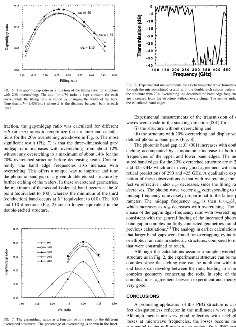
In the calculated photonic band structure~Fig. 4!, for the structure with optimized filling ratio, the top of the valence band occurs near the K point whereas the bottom of the conduction band is at the L point of the Brillouin zone. The experimental transmission of electromagnetic waves in the z direction normal to the Si wafers measures the band edges and gap at X
8
—the~001! point of the Brillouin zone. In the band-structure calculations the high-symmetry points were expressed in terms of the reciprocal lattice vectors ~G1, G2,and G3! of the body-centered orthorhombic lattice. For
ex-ample, the X
8
point is 0.5(G11G3), in this double-etchedstructure and in the fcc structure, representing transmission with a wave vector perpendicular to this stack. Similarly L is 0.5(G11G21G3). Such a convention for k points
elimi-nates the problems of traversing the reciprocal lattice in Car-tesian coordinates. For the experimental line spacing of
h5290mm and a bar width of 86mm a filling ratio of 0.297 is obtained. For a wafer thickness of 243mm, c is then 486
mm and c/h51.675. We note that there is some uncertainty
in the wafer thickness owing to spatial inhomogenity and decrease of wafer thickness during the processing steps, but the value of 243mm is supported by further characterization of the wafers. For c/h51.675, i.e., c/a51.15, we obtain cal-culated band edges of 277 and 388 GHz for transmission in the z direction, which agree very well with the measured values of 265 and 390 GHz ~Fig. 4!. In this direction the band edges are degenerate for both polarizations of the elec-tromagnetic wave. The calculated band structure in the 110 symmetry plane ~the plane containing both the rod and the normal to the rod! is shown in Fig. 5.
OVERETCHED STRUCTURE
The overetched unit cell geometry@Fig. 2~b!# was mod-eled most easily as two overlapping air rods in the silicon dielectric medium~e511.669!. Overetched regions of width 2d that determine the fraction of overetching ~2d/h! were introduced. The photonic bands were calculated as a function of filling ratio for fixed values of d. For each overetched
FIG. 3. Photonic gap/midgap ratio for the double-etched structure with no overetching@Fig. 2~a!# as a function of filling ratios. Each curve is for a different c/h aspect ratio.
FIG. 4. Experimental measurements for electromagnetic wave transmission through the micromachined crystal with the double-etched silicon wafers, corresponding to the structure in Fig. 1, with no overetching. The arrows indicate the calculated band edges.
FIG. 5. Photonic band structure for the double-etched structure with filling ratio 0.295 and c/h51.675 at the optimized gap/midgap geometry in Fig. 3. The X8point is~001! in the Brillouin zone. Waves normally incident along the z axis of the structure in Fig. 2~b! sample the GX8direction bands and measure the band gap at X8. Here c0is the speed of light, and a is the lattice
fraction, the gap/midgap ratio was calculated for different
c/h ~or c/a! ratios to reoptimize the structure and
calcula-tions for the 20% overetching are shown in Fig. 6. The most significant result ~Fig. 7! is that the three-dimensional gap/ midgap ratio increases with overetching from about 12% without any overetching to a maximum of about 14% for the 20% overetched structure before decreasing again. Concur-rently, the band edge frequencies also increase with overetching. This offers a unique way to improve and tune the photonic band gap of a given double-etched structure by further etching of the wafers. In these overetched geometries, the maximum of the second~valence! band occurs at the X point~equivalent to 100!, whereas the minimum of the third
~conduction! band occurs at X
9
~equivalent to 010!. The 100and 010 directions ~Fig. 2! are no longer equivalent in the double-etched structure.
Experimental measurements of the transmission of em waves were made in the stacking direction~001! for
~i! the structure without overetching and
~ii! the structure with 20% overetching and display
well-defined photonic band gaps~Fig. 8!.
The photonic band gap at X
8
~001! increases with double etching accompanied by a monotonic increase in both the frequencies of the upper and lower band edges. The mea-sured band edges for the 20% overetched structure are at 295 and 425 GHz which are in very good agreement with theo-retical predictions of 290 and 425 GHz. A qualitative expla-nation of these observations is that with overetching the ef-fective refractive index neffdecreases, since the filling ratiodecreases. The photon wave vector kmgcorresponding to the
midgap frequency is inversely proportional to the lattice pa-rameter. The midgap frequency vmg is then ~c/neff!kmg,
which increases as neff decreases with overetching. The
in-crease of the gap/midgap frequency ratio with overetching is consistent with the general finding of the increased photonic band gap in complex multiply connected geometries found in previous calculations.2,4The analogy in earlier calculations is that larger band gaps were found for overlapping cylindrical or elliptical air rods in dielectric structures, compared to rods that were constrained to touch.
Although the calculations assume a simple overetched structure as in Fig. 2, the experimental structure can be more complex since the etching rate can be nonlinear with time and facets can develop between the rods, leading to a more complex geometry connecting the rods. In spite of these complications, agreement between experiment and theory is very good.
CONCLUSIONS
A promising application of this PBG structure is a per-fect dissipationless reflector in the millimeter wave region. Although metals are very good reflectors with negligible losses at microwave frequencies, the losses become more substantial in the millimeter wave region. Such PBG struc-tures could have substantial advantage over metals in
milli-FIG. 6. The gap/midgap ratio as a function of the filling ratio for structure with 20% overetching. The c/a ~or c/h! ratio is kept constant for each curve, while the filling ratio is varied by changing the width of the bars. Note that c/h51.456(c/a) where h is the distance between bars in each layer.
FIG. 7. The gap/midgap ratios as a function of c/a ratio for the different overetched structures. The percentage of overetching is shown in the inset. For each c/a ratio~chosen points! the maximum gap was chosen by opti-mizing the filling ratio.
FIG. 8. Experimental measurements for electromagnetic wave transmission through the micromachined crystal with the double-etch silicon wafers, for the structure with 20% overetching. As described the band edge frequencies are increased from the structure without overetching. The arrows indicate the calculated band edges.
meter wave components. This PBG structure could be an ideal substrate for planar antennas that could substantially increase the antenna performance as has been proposed and measured10for microwave PBG structures. Such a reflecting substrate reflects all the antenna power in the forward direc-tion as is needed. Another applicadirec-tion of PBG structures is as a frequency selective filter. By introducing defects into peri-odic PBG structures, defect transmission peaks with very high Q within the band gap are produced. Such filters in the millimeter wave regime can efficiently select out frequencies of emission peaks needed in monitoring emission from gas-eous molecules such as in toxic gases. Such filters may also be very useful in millimeter wave astronomy.
In summary, we have designed and fabricated a new double-etched PBG structure that is robust, and has a sizable photonic gap/midgap ratio ~12%–14% for silicon! over a wide range of filling ratios and structural parameters. The new structure is a layer-by-layer structure with rods in each layer parallel to each other, whereas rods in successive layers are at an angle of 70.53° to each other. This represents a shearing of the previous layer-by-layer structures where rods in each successive layer were at an angle of 90° to each other. This new structure with the 70.53° angle can be real-ized by microfabrication techniques by etching the one-dimensional pattern on both sides of the Si wafer. For a fixed wafer thickness, the PBG frequency is approximately doubled from that possible by a single etching of the same Si-wafer. The new double-etched silicon wafers are mechani-cally more robust than the single-etched Si wafers.
Photonic band-structure calculations have been utilized to optimize the structural geometry to maximize the photonic gap. The overetching of the structure leads to an increase of the photonic gap consistent with general expectation of in-creased photonic gaps in multiply connected geometries. There is very good agreement between the calculated and measured PBG edges for double-etched structures, both with and without overetching. The overetched structure has been
experimentally fabricated and leads to a robust structure where the photonic midgap frequency can be easily tuned, in one direction, by further etching. This system has yielded among the highest midgap frequencies obtained to date and is promising for extending the PBG frequencies into the IR region.
ACKNOWLEDGMENTS
We thank J. Bostak and D. M. Bloom for measurements at Stanford University. We thank C. M. Soukoulis, M. Siga-las, C. T. Chan, and G. Tuttle for several helpful discussions. This work was partially supported by the Center for Ad-vanced Technology ~CATD! through funding from the De-partment of Commerce. This work was also supported by the Director for Energy Research, Office of Basic Energy Sci-ences and Advanced Energy Projects. The Ames Laboratory is operated for the U. S. Department of Energy by Iowa State University under Contract No. W-7405-Eng-82.
1
For a recent review, see Photonic Bandgaps and Localization, edited by C. M. Soukoulis~Plenum, New York, 1993!.
2K. M. Ho, C. T. Chan, and C. M. Soukoulis, Phys. Rev. Lett. 65, 3152 ~1990!.
3
E. Yablonovitch, T. J. Gmitter, and K. M. Leung, Phys. Rev. Lett. 67, 2295~1991!.
4K. M. Ho, C. T. Chan, C. M. Soukoulis, R. Biswas, and M. Sigalas, Solid
State Commun. 89, 413~1994!.
5E. Ozbay, A. Abeyta, G. Tuttle, M. Tringides, R. Biswas, M. Sigalas, C.
M. Soukoulis, C. T. Chan, and K. M. Ho, Phys. Rev. B 50, 1945~1994!.
6E. Ozbay, G. Tuttle, R. Biswas, M. Sigalas, and K. M. Ho, Appl. Phys.
Lett. 64, 2059~1994!.
7E. Ozbay, E. Michel, G. Tuttle, R. Biswas, K. M. Ho, J. Bostak, and D. M.
Bloom, Opt. Lett. 19, 1155~1994!.
8
S. Fan, P. R. Villeneuve, R. D. Meade, and J. D. Joannopoulos, Appl. Phys. Lett. 65, 1466~1994!.
9E. Ozbay, G. Tuttle, R. Biswas, K. M. Ho, J. Bostak, and D. M. Bloom,
Appl. Phys. Lett. 65, 1619~1994!.
10
E. R. Brown, C. D. Parker, and E. J. Yablonovitch, J. Opt. Soc. Am. B10, 404~1993!; E. R. Brown, C. D. Parker, and O. B. McMahon, Appl. Phys. Lett. 64, 3345~1994!.