INVESTIGATION OF BIAS-ASSISTED
PHOTOENHANCED ELECTROCHEMICAL ETCHING
FOR FABRICATION OF SELF-ALIGNED GALLIUM
NITRIDE BASED BIPOLAR TRANSISTORS
a thesis
submitted to the department of electrical and
electronics engineering
and the institute of engineering and sciences
of bilkent university
in partial fulfillment of the requirements
for the degree of
master of science
By
Emre Alptekin
August 2006
I certify that I have read this thesis and that in my opinion it is fully adequate, in scope and in quality, as a thesis for the degree of Master of Science.
Assist. Prof. Dr. ¨Ozg¨ur Akta¸s (Supervisor)
I certify that I have read this thesis and that in my opinion it is fully adequate, in scope and in quality, as a thesis for the degree of Master of Science.
Prof. Dr. Cengiz Be¸sikci
I certify that I have read this thesis and that in my opinion it is fully adequate, in scope and in quality, as a thesis for the degree of Master of Science.
I certify that I have read this thesis and that in my opinion it is fully adequate, in scope and in quality, as a thesis for the degree of Master of Science.
Dr. Tarık Reyhan
I certify that I have read this thesis and that in my opinion it is fully adequate, in scope and in quality, as a thesis for the degree of Master of Science.
Assist. Prof. Dr. Ceyhun Bulutay
Approved for the Institute of Engineering and Sciences:
Prof. Dr. Mehmet Baray
ABSTRACT
INVESTIGATION OF BIAS-ASSISTED
PHOTOENHANCED ELECTROCHEMICAL ETCHING
FOR FABRICATION OF SELF-ALIGNED GALLIUM
NITRIDE BASED BIPOLAR TRANSISTORS
Emre Alptekin
M.S. in Electrical and Electronics Engineering
Supervisor: Assist. Prof. Dr. ¨
Ozg¨ur Akta¸s
August 2006
GaN-based bipolar transistors are good candidates for applications in RF power amplifiers. In contrast to more common AlGaN/GaN high electron mobility tran-sistors (HEMTs), GaN based bipolar trantran-sistors have not drawn much attention because of the difficulties in good p-type material and ohmic contact. Most of the problems associated with p-type quality and contact come from growth and etch damage during fabrication.
In this work, a low damage etching technique with an undercut profile was developed to solve the problems associated with p-type ohmic contact quality and to realize the self-aligned GaN bipolar transistor fabrication. The etching process consists of bias-assisted photoenhanced electrochemical oxidation of GaN in deionized water (BPECO/DI) and its subsequent etching in diluted acid so-lution. By this technique, we demonstrated good Schottky contacts on samples
it was also obtained by BPECO/DI etching. Hence this technique is ideal for fabrication of self-aligned bipolar transistors.
There are some problems during fabrication of self-aligned bipolar transis-tor. First, due to the impossibility of activation annealing after emitter etch, activation annealing had to be done at the beginning where emitter layer is on the base and this was a problem for Mg activation. More importantly, there were still uncertainties with BPECO/DI etching like roughening up the etched surface, low etch rate for npn structures and disturbing the material uniformity near the surface.
In this work, it was shown that BPECO/DI etching is a very efficient tool that provided low damage etching of GaN and enabled the self aligned RF bipolar transistor structures. It was found that self aligned base-emitter junctions were successfully formed and the BPECO/DI etching was almost stopped at top of the base layer. Self-aligned bipolar transistors were fabricated and their base-emitter and base-collector junctions were measured. The results obtained in this work demonstrated that BPECO/DI etching can bring solutions to the lack of low damage etching and the impossibility of self-aligned base contact in fabrication of today’s GaN based bipolar transistors.
Keywords: Gallium nitride, bipolar transistor, photo-enhanced electrochemical
¨
OZET
KEND˙INDEN YERLES¸MEL˙I GALYUM N˙ITR˙IT TABANLI ˙IK˙I
KUTUPLU TRANS˙IST ¨
ORLER˙IN FABR˙IKASYONU ˙IC
¸ ˙IN
POTANS˙IYEL YARDIMLI FOTON KATKILI
ELEKTROK˙IMYASAL AS¸INDIRMA
Emre Alptekin
Elektrik ve Elektronik M¨uhendisli¯gi B¨ol¨um¨u Y¨uksek Lisans
Tez Y¨oneticisi: Assist. Prof. Dr. ¨
Ozg¨ur Akta¸s
A˘gustos 2006
GaN tabanlı iki kutuplu transist¨orler RF g¨u¸c y¨ukselteci uygulamaları i¸cin iyi adaylardır. ˙Iyi p-tipi materyal b¨uy¨utmedeki ve p-tipi ¨uzerine iyi kontak yap-madaki g¨u¸cl¨uklerden dolayı, GaN tabanlı iki kutuplu transist¨orler, AlGaN/GaN y¨uksek elektron hareketlilikli transist¨orler kadar ilgi toplamamı¸stırlar. P-tipi kalitesi ve kontak yapmadaki problemlerin ¸co˘gu b¨uy¨utmeden ve fabrikasyon a¸samasındaki a¸sındırma hasarından kaynaklanmaktadır.
Bu ¸calı¸smada, p-tipi kontak kalitesiyle ilgili sorunları ¸c¨ozmek i¸cin az hasarlı bir a¸sındırma tekni˘gi geli¸stirilmi¸stir. A¸sındırma i¸slemi potansiyel destekli fo-toelektrokimyasal oksitleme ve ardından gelen seyreltilmi¸s asit i¸cinde bu ok-sitin kaldırılmasından olu¸sur. Bu teknikle, 100 nm’den daha fazla a¸sındırılmı¸s y¨uzeyler ¨uzerine iyi Schottky kontaklar yapılmı¸stır ve bu a¸sındırmanın p/n katkılı katmanlardaki se¸cicili˘gi g¨osterilmi¸stir. Bununla beraber, kendinden yerle¸smeli fabrikasyon i¸cin en kritik nokta olan negatif e˘gimli a¸sındırmanın,
idealdir. Sonu¸c olarak, bu teknikle transist¨or karakteristikleri ¨onemli ¨ol¸c¨ude iy-ile¸stirilebilinir.
Kendinden yerle¸smeli transist¨or fabrikasyonunda bazı sorunlar vardır. ˙Ilk olarak aktivasyon tavlamasının yayıcı a¸sındırmasından sonra yapılmasının m¨umk¨un olmamasından dolayı aktivasyon a¸sındırması taban ¨uzerinde yayıcı kat-manı varken yapılmak zorundadır ve bu Mg aktivasyonu i¸cin bir problemdir. Daha ¨onemlisi y¨uzey p¨ur¨uzl¨ul¨u˘g¨u, npn katmanların d¨u¸s¨uk a¸sındırılma hızı ve materyal y¨uzeyinin d¨uzg¨unl¨u˘g¨un¨un bozulması gibi BPECO/DI a¸sındırmada halen belirsizlikler mevcuttur.
Bu ¸calı¸smada BPECO/DI a¸sındırmanın, GaN i¸cin az hasarlı bir a¸sındırma y¨ontemi oldu˘gu ve kendinden yerle¸smeli RF iki kutuplu transist¨or fabrikasyonunu m¨umk¨un kıldı˘gı g¨osterilmi¸stir. Taban-yayıcı ba˘glantısı ba¸sarıyla kurulmu¸stur ve BPECO/DI a¸sındırmanın taban katmanında durdu˘guda g¨osterilmi¸stir. Kendin-den yerle¸smeli iki kutuplu transist¨orler ba¸sarılı bir ¸sekilde fabrike edilmi¸s ve taban-yayıcı ve taban-toplayıcı ba˘glantıları akım voltaj karakteristikleri ¨ol¸c¨ulm¨u¸st¨ur. Bu ¸calı¸smadaki sonu¸cların BPECO/DI a¸sındırmanın bug¨unk¨u GaN tabanlı iki kutuplu transist¨or fabrikasyonu i¸cin az hasarlı a¸sındma y¨ontemi yoklu˘guna ve kendinden yerle¸smeli taban konta˘gı kurmaya ¸c¨oz¨um getirdi˘gi g¨osterilmi¸stir.
Anahtar Kelimeler: Galyum nitrat, iki kutuplu transist¨or, ı¸sık katkılı
ACKNOWLEDGMENTS
I would like to express my sincere gratitude to my supervisor Assist. Prof. Dr. ¨Ozg¨ur Akta¸s. His personal and academic virtue has shaped my academic personality and my approach to science. It was a great chance and pleasure for me to study under his supervision. This work would not be possible without his guide and encouragements.
I would like to thank to the members of my thesis committee, Prof. Cengiz Be¸sik¸ci, Assist. Prof. Mehdi Fardmanesh, Dr. Tarik Reyhan and Assist. Prof. Ceyhun Bulutay for reading the manuscript and commenting on the thesis.
I would like to express my special thanks to Murat G¨ure, Erg¨un Hırlako˘glu, S. Ersin Ba¸sar and Erg¨un Karaman, for their support and help.
I want to thank A¸skın Kocaba¸s for his support and numerous fruitful discus-sions on experiments.
Special thanks belong to my family, for their nonstop support and care. I dedicate this labor to them.
Finally, I would like to acknowledge the financial support from TUBITAK that made this work possible.
Contents
1 Introduction 1
1.1 Motivation for GaN based bipolar transistors . . . 1
1.2 The objective and scope of the thesis . . . 4
2 Theory and Design 5
2.1 Basics of Schottky Diodes . . . 5
2.2 Basics of Bipolar Transistors . . . 9
3 Bias-Assisted Photoenhanced Electrochemical Oxidation in
Deionized Water 13
3.1 Experimental Setup . . . 15
3.2 Experiment . . . 17
3.3 Experimental Results . . . 18
4 Fabrication of Bipolar Transistors 21
4.2 Process Steps . . . 22 4.2.1 Sample Preparation . . . 22 4.2.2 Lithography . . . 23 4.2.3 Etching . . . 24 4.2.4 Metallization . . . 25 4.2.5 Annealing . . . 26
4.3 Bipolar Transistor Fabrication Process . . . 26
4.3.1 Activation Annealing . . . 26 4.3.2 Emitter Contact . . . 27 4.3.3 Base Etch . . . 28 4.3.4 Base Contact . . . 29 4.3.5 Collector Etch . . . 29 4.3.6 Collector Contact . . . 29 4.3.7 Mesa Isolation . . . 29 4.3.8 Post Formation . . . 30
4.3.9 Air Bridge Process . . . 30
4.3.10 Planarization . . . 30
5.1 Schottky Measurements and Results . . . 34
5.2 Bipolar Transistor Measurements and Results . . . 42
List of Figures
2.1 Energy band diagrams of metal contact to n-type (a) and p-type (b) semiconductor under thermal equilibrium. . . 6
2.2 Conduction mechanisms for metal-semiconductor contact under very small bias (a), reverse bias (b), forward bias (c) . . . 8
2.3 Bipolar transistor operation at forward active mode. . . 10
3.1 Different band bending of n- and p-type GaN/electrolyte interface 15
3.2 The experiment setup of BPECO/DI etching system . . . 16
3.3 An SEM image of the Ti/Al/Ni/Au metalization undercut by the BPECO/DI etching. . . 19
4.1 Structure of Bipolar Junction Transistor . . . 22
4.2 Self-aligned metallization on a)positive and b)negative slope etched surfaces . . . 25
4.3 Bipolar junction transistor device structure . . . 27
4.5 The device after air bridge process (top) and the air bridge con-necting the base to the base hill (bottom) . . . 32
4.6 The final view of the fabricated device . . . 33
5.1 Reverse current-voltage characteristics of Schottky contacts fabri-cated on surfaces after various treatments. . . 35
5.2 Forward current-voltage characteristics of Schottky contacts fab-ricated on surfaces after various treatments. . . 35
5.3 The 1/C2 as a function of bias for a Schottky structure a) on
untreated surface b) on surface etched by PEC oxidation at 6 V for 120 minute c) on surface etched as in b) and annealed as described in the text. . . 37
5.4 I-V characteristics of 7µm TLM pattern on control, BPECO/DI etched and RIE etched surfaces . . . 39
5.5 I-V Characteristics of 6 µm TLM on the base region . . . 42
5.6 I-V Characteristics of base-emitter junction in linear scale (top) and logarithmic scale (bottom) . . . 44
5.7 I-V Characteristics of base-collector junction in linear scale (top) and logarithmic scale (bottom) . . . 45
5.8 I-V Characteristics of TLM patterns on sample intentionally etched less than emitter thickness in linear scale (top) and log-arithmic scale (bottom) . . . 46
List of Tables
1.1 Figures of merit for different materials. . . 2
3.1 Oxide thicknesses and etch depths measured at different oxidation conditions. . . 18
3.2 Atomic concentration percentages as measured by Auger electron spectroscopy on samples at various stages of etching process. . . . 19
5.1 Characteristics of Schottky contacts fabricated on GaN surfaces with various treatments. . . 34
Chapter 1
Introduction
1.1
Motivation for GaN based bipolar
transis-tors
The material system GaN has pioneered wide application area in optoelectron-ics. Its direct and wide band gap have made GaN based optoelectronic devices at green to ultraviolet spectrum possible [1]. In addition to superior GaN op-toelectronic devices, the electronics applications based on GaN have shown very promising performance. Especially in the area of amplifiers for communications and military purposes, GaN high electron mobility transistors, HEMTs, have demonstrated high speed and high power performance [2, 3, 4]. Also in appli-cation of low loss and high power switches, GaN based devices are widely used.
GaN has a relatively large band gap of 3.47 eV, a very high breakdown field 3.3 MV/cm and a high saturation velocity of 1.9x10⁷cms−1 [5, 6]. All these
properties make GaN a good candidate for high power and high speed applica-tions.
Together with its good characteristics, alloys of GaN are also utilized in device engineering. InGaN and AlGaN materials offer a wide range of band gap 0.8 eV to 6.2 eV. This enables to design and fabricate novel devices.
The most interesting feature of GaN and its alloys is their highly piezoelec-tric structure offering devices not possible with other III-V material systems like GaAs or InP. A two dimensional electron gas (2DEG) region forms when AlGaN/GaN heterostructures are grown. This highly concentrated and high mobility region lead to the fabrication of today’s superior HEMT devices.
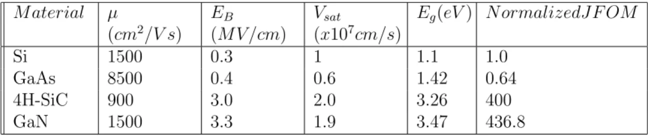
Comparison of semiconductor materials figures of merit is an efficient way to find out their device characteristics. Power handling, power loss and RF performance of a semiconductor material can be estimated from its figures of merit. The Johnson’s figure of merit, JFOM=(vsatEB/2π)2 is a merit for RF
performances like cutoff frequency (fc) and maximum power handling capacity.
Since it relates saturation velocity and breakdown voltage, it demonstrates the high power and high frequency capability of material. In Table 1.1, normalized JFOMs for different materials are given and normalization is done by setting JFOM of Si to 1. It is seen that in high power and high frequency applications GaN based devices capability is much better than Si and GaAs, and better than 4H-SiC. Material µ (cm2/V s) EB (MV /cm) Vsat (x107cm/s) Eg(eV ) NormalizedJF OM Si 1500 0.3 1 1.1 1.0 GaAs 8500 0.4 0.6 1.42 0.64 4H-SiC 900 3.0 2.0 3.26 400 GaN 1500 3.3 1.9 3.47 436.8
Table 1.1: Figures of merit for different materials.
High power handling of GaN power transistors have already been demon-strated by fabrication of GaN high electron mobility transistor (HEMT) and field effect transistor (FET) devices. Although the progress of GaN field effect
transistors is impressive, advances in GaN bipolar transistor has been slowed down by the difficulties associated with GaN p-type material. The motivation behind bipolar transistors is the inherent device characteristics of higher power handling capacity, linearity, higher transconductance and uniform turn-on volt-age. Furthermore surface problems which most FET devices suffer from do not affect bipolar transistor characteristics that much.
In the literature, AlGaN/GaN and InGaN/GaN based bipolar transistors were fabricated with dc current gains of 1.5 to 10 [7, 8, 9]. Transistor fabrication methods require base regrowth to renew the etched surface so that better contacts can be achieved. However regrowth is a complex, tedious and difficult process, some other fabrication methods are demanded in order to overcome etch damage. BPECO/DI etching can be a tool for the required etching method. We have demonstrated that BPECO/DI etching is a low damage etching method and p-type contacts on BPECO/DI etched surfaces are much better than plasma etched surfaces.
Furthermore BPECO/DI etching is an isotropic etching and this provides undercut profile after etching that is not possible with dry etching methods. This undercut profile makes self aligned transistor fabrication possible. Self aligned fabrication is a key for RF device fabrication. There was no self aligned bipolar transistor fabricated yet due to the unavailability of etching that both gives undercut and does not attack metal contacts.
We have demonstrated that these two features of BPECO/DI etching can solve two problems in fabrication of bipolar transistors. To sum up, by using BPECO/DI etching, self aligned bipolar transistors were fabricated.
1.2
The objective and scope of the thesis
In this work, a low damage wet etching method bias assisted photoelectrochemi-cal oxidation in deionized water (BPECO/DI) is introduced and then it is utilized in bipolar GaN transistor fabrication for the first time in literature.
The thesis consists of 6 chapters. Chapter 1 contains the introduction and motivation. In chapter 2, the theory of Schottky diode and bipolar transistor are described.
Chapter 3 explains the BPECO/DI etching experiment setup and its exper-imental results. Fabrication methods and bipolar transistor fabrication process are given in chapter 4.
Chapter 5 goes into the experimental results of Schottky contacts on etched surfaces by low damage etching method BPECO/DI etching and results for fab-ricated GaN based bipolar transistors. Finally, chapter 6 contains the discussions regarding this work and conclusion.
Chapter 2
Theory and Design
2.1
Basics of Schottky Diodes
In surface damage studies due to etching mechanisms, comparison of Schottky diode characteristics is an efficient and commonly used way [10, 11, 12]. In order to analyze the damage, we have compared Schottky characteristics of contacts on etched and unetched surfaces [13]. To understand the effects of damage, it is essential to know the metal-semiconductor contact properties and the causes behind their changes. Hence, in this section, we will give some introductory knowledge on Schottky contacts, analysis of the forward and reverse character-istics, and some mechanisms for their changes.
Rectifying metal-semiconductor contact is named Schottky after W. Schottky proposed a model for barrier formation in 1931 [14]. When a metal is contacted with a semiconductor, a potential barrier is formed due to separation of charges at the metal-semiconductor interface. Energy band diagrams of Schottky contacts on n- and p-type contacts under thermal equilibrium are given in Figure 2.1.
Figure 2.1: Energy band diagrams of metal contact to n-type (a) and p-type (b) semiconductor under thermal equilibrium.
Because of the thermionic electron emission over the barrier, the current-voltage characteristic is given by the relation,
I = Is[exp(
qV
nkT) − 1] (2.1)
where Is, n and A∗ are the reverse saturation current, ideality factor and the
modified Richardson constant, respectively. The formula implies that the diode reverse current saturates and the forward current increases exponentially with applied bias. However, in experimental results, there are deficiencies from ideal due to surface states, traps, field emission (FE), thermionic field emission (TFE), surface roughness, inhomogeneity in Schottky barrier heights and other damage mechanisms during fabrication.
Although dry etching systems cause more damage than wet etching systems due to damage created by highly energetic atoms, both etching systems can result in change of surface morphology by changing the crystal structure of surface, by depositing etching residues, by forming interface layers or by creating antisites on the surface. These surface deficiencies can significantly affect the Schottky diode characteristics [10, 11, 12].
The reverse characteristics like reverse breakdown voltage and leakage cur-rent degrade with damage mechanisms, and these can be improved by various treatment methods. The trap assisted tunnelling, hopping through the increased surface states, surface roughening, barrier lowering, barrier inhomogeneity due to surface nonuniformity or antisites can increase the reverse current. These also degrades the breakdown voltage. Various treatments like low damage wet etch-ing [15], annealetch-ing [16] or surface passivation [17] were tried to get the original characteristics back.
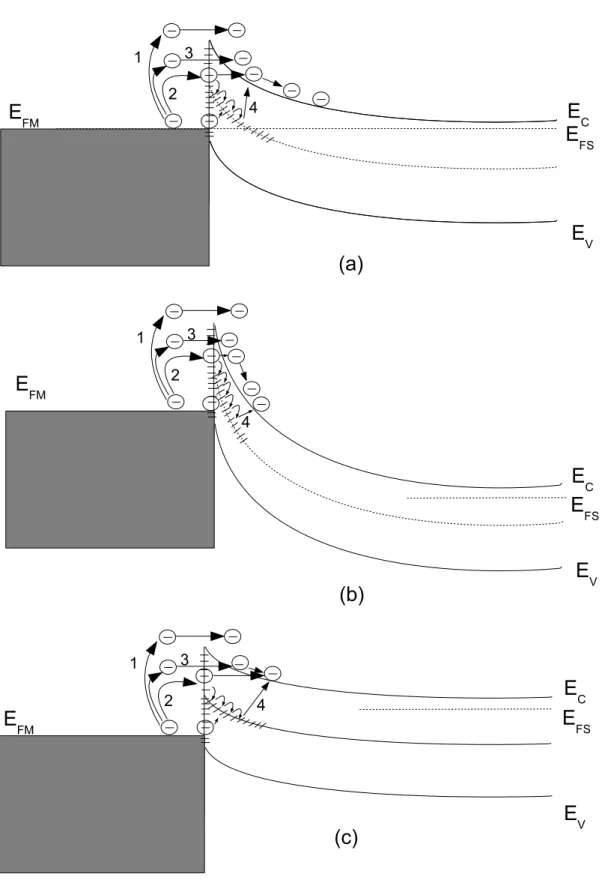
While the observations on leakage current and breakdown voltage are not anomalous, there are conflicted observations on ideality factor. One explanation for the anomaly in ideality factor is given by Tung [18] as nonuniform Schottky barrier height. In order to understand the reason for anomaly in ideality factor, we should examine the current transport mechanisms for metal-semiconductor interfaces. In Figures 2.2, a metal-semiconductor interface at different biases are given. There are 4 conduction mechanism shown (1. Thermionic emission, 2. Tunneling through surface traps, 3. Field emission (and thermionic field emis-sion) tunneling, 4. Hopping through the deep trap states). From thermionic emission model, thermionic emission current saturates at reverse biases and ex-ponentially increases with forward bias voltages. In ideal diodes, only this current transport is taken into account and the other mechanisms are ignored. However in real life this is not so.
In Figure 2.2-a, if very small biases are applied, the dominant current mecha-nism depends on temperature and the density of the surface states. If the diode is near ideal, then second and third mechanisms can be ignored. And in this case, if the temperature is low then field emission tunneling dominates and for moderate temperatures both conduction mechanisms contribute to the current conduction.
Figure 2.2: Conduction mechanisms for metal-semiconductor contact under very small bias (a), reverse bias (b), forward bias (c)
At reverse bias voltages, as seen in Figure 2.2-b, since the barrier thickness decreases significantly, tunneling through near surface states and field emission tunneling mechanisms, that exponentially depend the barrier thickness, dominate the overall current.
At forward bias voltages, as seen in Figure 2.2-c, in contrast to reverse bias conduction, effect of tunneling through near surface states and field emission tunneling mechanisms decreases. Therefore the dominant mechanisms become thermionic emission current and hopping through the deep trap states.
Some damage mechanisms can create both deep traps and surface states. Treatments like annealing or H2 plasma passivate the surface states and cannot
improve the deep traps in the bulk. Hence, while ideality factor is not improved, the reverse characteristics improve after treatments. In other words, the anomaly in ideality factor lies under different damage mechanisms than near surface states.
2.2
Basics of Bipolar Transistors
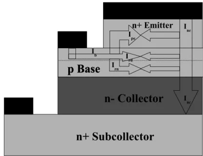
Explanation of principles of bipolar transistors can be readily found in textbooks [19]. To follow the main idea of this work, a brief summary of operation of bipolar transistors is given in the following.
In Figure 2.3, a bipolar transistor schematic is given where the basic forward active operation of a bipolar transistor is illustrated. In forward active operation, base-emitter junction is forward biased and base-collector junction is reverse biased. By forward biasing base-emitter junction, electrons are emitted from emitter to base and holes are emitted from base to emitter. These holes injected to the emitter form one base current component (Ipe). Then some of electrons
Figure 2.3: Bipolar transistor operation at forward active mode.
components of base current. Since the current diffuses to collector region is too low compared to the terms mentioned above , it can be neglected. Therefore, the base current can be given by three components.
Ib = Ipe+ Ird+ Irn (2.2)
There are two important parameters defined γ and αT, emitter injection
coeffi-cient and base transport factor. The emitter injection coefficoeffi-cient γ is defined as the ratio of current injected to base to total emitter current.
γ = Ine Ine+ Ird+ Ipe
(2.3)
From the equation above, having an efficient emitter requires to have Ird+ Ipe
much smaller than Ine. It can be satisfied, by designing emitter doping much
higher than base doping or using heterostructure where the offset between base and emitter valance bands provides a barrier to avoid holes to diffuse into emit-ter region. On the other hand, Ird depends on the material type and quality.
Since GaN is a direct band gap material and its p-type is problematic, this term dominates the base current and results in large base currents.
The base transport factor αT is defined as the ratio of current reaching to
collector to current injected from base.
αT = Inc
Ine
(2.4)
The difference between the current terms, Incand Ineis the recombination current
in the neutral base region. Hence the quality and thickness of the base material have significant effects on both transport parameters.
The common base current gain α and the common emitter current gain β are the most important DC parameters in bipolar transistor characterization. As in Equation (2.5) and (2.6), α is the ratio of collector current to emitter current and β is the ratio of collector current to base current.
α = γαT (2.5)
β = α
1 − α (2.6)
In bipolar transistor design, the device structure thicknesses and doping levels are needed to be optimized to improve current gain β, breakdown voltage VB
and RF performance of the device.
As given in Equation (2.5) and (2.6) to increase β, the emitter injection coef-ficient and base transport factor are demanded. The emitter injection coefcoef-ficient can be improved by engineering AlGaN/GaN or GaN/InGaN heterostructures. The wider band gap emitter blocks hole current from base to emitter and this increases γ. On the other hand, good base transport factor requires thin base and large Dn. Thin base and large Dn decreases the recombination in neutral
region and gets αT closer to 1.
Together with the above design criterions, the base material quality and the low damage etching mechanisms are essential to improve both γ and αT. The
doping grading. As τndecreases, cut-off frequency of the device is also improved.
Finally, the base material quality and low damage etching are very critical to obtain high β’s and good RF results.
Chapter 3
Bias-Assisted Photoenhanced
Electrochemical Oxidation in
Deionized Water
GaN dry etch process is well established for electronic and photonic device fab-rications. There are several plasma etching systems like electron cyclotron res-onance (ECR), inductively coupled plasma (ICP), chemically assisted ion beam etching, and reactively ion beam etching (RIE). The common properties of these plasma etching systems are high etch rates and uniform etching properties. How-ever, plasma etching results in significant surface damage that degrades optical and electronic properties of material. There can be three results of plasma etch-ing on the etched surface; 1) Deposition of residue on the surface, 2) Diffusion of the plasma constituents or etching products, and 3) Generation of defects in the crystal lattice. These surface damage mechanisms result in leakage cur-rent by creating traps and these traps increase the tunnelling curcur-rent between semiconductor and metal deposited on the surface.
Techniques for low-damage etching of GaN and its alloys are important for optimization of devices such as HEMTs and HBTs [20, 21, 22, 23]. Ultravi-olet photoenhanced electrochemical (PEC) etching and oxidation of GaN is a versatile method that is both band-gap and doping selective [24, 25, 26, 27]. PEC etching can achieve a smooth surface with low etch damage [28, 29]. A process similar to PEC etching and oxidation of GaN in alkaline solutions is the bias-assisted photoenhanced electrochemical oxidation of GaN in deionized water (BPECO/DI) [30]. In this approach, the oxide that forms on the surface remains intact and thick oxide layers can be obtained. To achieve etching of the GaN surface, the oxide grown by BPECO/DI can be removed by an HCl or HF etch following the oxidation. In this study, the etching process employing bias-assisted photoenhanced electrochemical oxidation in DI water and a subsequent acid bath removal of the oxide is called ”BPECO/DI etch”.
Similar to the PEC etching in alkaline solutions, the BPECO/DI etching process is attractive due to the band gap and n/p doping selectivity that can be achieved. However, this process has additional advantages that the BPECO/DI oxidation and etching can be performed with a photoresist mask in place and also without damaging existing ohmic or Schottky metalization on the sample. Catalytic titanium masks are not needed for BPECO/DI etching and the process can be applied to relatively large areas. Hence, the process does not suffer from the inhomogeneities commonly observed close to the titanium mask edges used with PEC and bias-assisted PEC (BPEC) processes. Thus, BPECO/DI etching has the potential to be a technique that is more widely applied than PEC etching.
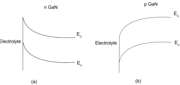
Doping selective etching by BPECO/DI etching was achieved. The different band bending for n- and p-type GaN materials, as seen in Figure 3.1, explains the reason behind the selectivity. Since n-type material band at the semicon-ductor/electrolyte interface bends upwards, holes prefer to move to the surface. However in p-type material, due to downward band bending, holes are taken
Figure 3.1: Different band bending of n- and p-type GaN/electrolyte interface away from the surface. In other words, to accumulate holes on the p-type mate-rial surface, more potential is needed.
2GaN + 6h++ 6OH− −→ Ga2O3+ 3H2O + N2 ↑ (3.1)
Oxide formation mechanism is given by Equation 3.1. As it is seen, the photo-generated holes are essential for oxide formation. The oxidation products are Ga2O3, 3H2O and N2. Due to the reaction product N2, bubbles going out
from the sample surface were observed during the oxidation .
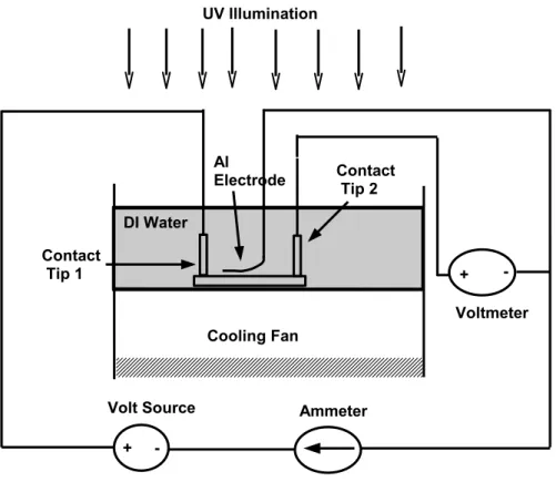
3.1
Experimental Setup
The BPECO/DI oxidation setup is given in Figure 3.2. The sample is biased in deionized (DI) water in the range of 4 to 20 Volts and the light from a 200 W Hg-Xe UV lamp was focused by an elliptical mirror. The sample was placed close to the focal point. We have used Al as counter electrode. And in case of oxidation
Figure 3.2: The experiment setup of BPECO/DI etching system
methods were tried to have contact to the sample, but the most convenient way was found a nickel coated iron tip. The coating nickel is to prevent the corrosion. During oxidation, the voltage on the sample and the current passing through were measured to ensure that the contact to the sample was not lost and to record the current during oxidation. The oxidation time was limited by thickness of the undoped layer and was selected to be 3 hours after preliminary tests. The water level was almost the same for all experiments and it was 1 cm above the sample surface. Also in long oxidation times, the water evaporated by UV light was refreshed by adding new DI water so that the water level was kept constant. The DI water resistance was more than 13 MΩcm for all the oxidation experiments.
3.2
Experiment
The layer structure used in this study consisted of a 0.5 µm undoped GaN layer grown on top of 0.5 µm and 2x1018cm−3 Si doped GaN layer at the bottom. All
samples were grown on sapphire substrates using MOCVD. Before the oxidation of the samples with BPECO/DI, mesa etching and ohmic contact fabrication steps were completed. The mesa structures were needed for establishing ohmic contacts to the highly doped GaN layer. A few of the mesa structures were partially masked with sputtered SixNy to enable etch depth measurement. For
the collection of photogenerated electrons, 1 mm wide ohmic contact metalization was fabricated on the four edges of the samples.
In order to measure the BPECO/DI oxide thickness, the top of the mesa structures were patterned by photoresist following BPECO/DI oxidation, and the oxide was etched from the exposed areas by a 1:5 HCl:DI etch. After the measurement of the oxide thickness from the exposed edge by using a profilome-ter, the photoresist mask was removed and all of the remaining oxide on the surface was etched. Next, in order to measure the etch depth, the SixNy mask
was removed by a 1:100 HF:DI etch and the etch depth was measured from the exposed edge on top of the mesa structures. Some of the samples were an-nealed at 700 ◦C for 30 seconds in an effort to remove the BPECO/DI etch
damage. As a final step, Ni/Au (45/50 nm) Schottky structures were patterned and evaporated on the mesas. Immediately before loading of the samples to the evaporator for Ni/Au evaporation, the samples were dipped to 1:2 HCl:DI solution for 30 seconds, rinsed, and blown dry with nitrogen. AES and AFM measurements were taken from bare samples without mesas and Schottky struc-tures, but with the BPECO/DI contact metalization in place on four edges of the sample. Capacitance-voltage measurements were done using an HP-4284 LCR meter at 10 and 100 kHz. AES measurements were performed on a PHI 660
scanning Auger microprobe. The AES spectra was taken from a 5x5 micron area on the surface. All measurement results are given in Chapter 5.
3.3
Experimental Results
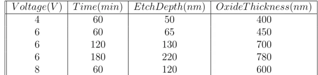
V oltage(V ) T ime(min) EtchDepth(nm) OxideT hickness(nm)
4 60 50 400
6 60 65 450
6 120 130 700
6 180 220 780
8 60 120 600
Table 3.1: Oxide thicknesses and etch depths measured at different oxidation conditions.
Etch depth versus time and voltage data obtained as described above are given in Table 3.1. The etch depths and oxide thicknesses given in Table 3.1 were measured from the top of the mesa structures as noted above. In earlier work [30], saturation of oxide thickness with time was observed to set in after 1 hour of oxidation and the saturated oxide thickness reported at 5 V bias was 175 nm. In the present study, a similar saturation of oxide thickness is observed. However, it takes about 2 hours for strong saturation to be observed, and the resulting oxide thickness is much larger. Crucially, it needs to be noted that the etch depth saturation was not observed at the maximum feasible etching time, despite the strong saturation observed in the oxide thickness. Otherwise, we can observe that the etch rate increases with increasing anode bias, and in general stays in the same range as the values reported in earlier work [30].
The undercutting of annealed Ti/Al/Ni/Au ohmic pads were observed by scanning electron microscopy. A representative image is shown in Figure 3.3, where the undercutting of the metalization is clearly observed. For this spe-cific sample, the oxidation was performed for 60 minutes under 10 V bias. The
Figure 3.3: An SEM image of the Ti/Al/Ni/Au metalization undercut by the BPECO/DI etching.
roughness observed on top of the metalization is typical of Ti/Al/Ni/Au and other Ti/Al based annealed ohmic contacts to GaN. The roughness of the etched surface can also be seen in Figure 3.3.
Ga N O C S Cl As grown 40.1 40.3 10 8.1 1.5 -Oxidized 34.4 - 58.8 6.7 - -Oxidized etched 37.9 37.9 11.9 11.9 - 0.4 Oxidized etched and annealed 34.4 32.3 12.8 19.7 0.5 0.3
Table 3.2: Atomic concentration percentages as measured by Auger electron spectroscopy on samples at various stages of etching process.
The relative percentages of atoms on the surface given by AES is shown in Table 3.2. It is seen that oxidation results in a surface without any nitrogen
seen that, annealing of the etched sample did not create a significant change in atomic percentages.
Besides p-type etching tests were performed. A p-type layer of 1.0 µm thick and 2x1019 cm−3 Mg doped was used in these tests. Prior to BPECO/DI
oxi-dation, for activation, the layer was annealed at 750 ◦C for 20 minutes. It was
observed that the p-type material was etched at bias voltages more than 12 V while n-type material etch was done over 4 V. This implies that by biasing the sample between 4 to 12 Volts, p/n selective etching is achieved.
Chapter 4
Fabrication of Bipolar
Transistors
The fabrication process of self-aligned bipolar transistor consists of 10 steps. These steps are emitter metallization, base etch, base metallization, collector etch, collector metallization, mesa isolation, post formation, air bridge metalliza-tion, planarization and RF pad formation. In this fabricametalliza-tion, the most critical point is the low damage base etching and self-aligned base contact formation. It was demonstrated that BPECO/DI etching is a low damage etching method and gives undercut that makes the self-aligned base contact possible. Hence, we have managed to fabricate low damage and self-aligned base contacts by engineering BPECO/DI etching.
4.1
Metal Organic Chemical Vapor Deposition
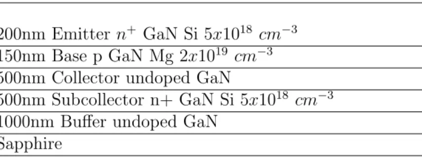
in this work were grown in the MOCVD machine located in Nanotam Research Center in Bilkent University. All GaN bipolar transistor structures were grown on sapphire substrates. An unintentionally doped buffer layer was first grown and followed by an n-type subcollector and an unintentionally doped collector. Then a p-type Mg doped base and n+ emitter layers were grown. The carrier concentrations for the emitter, base and collector were estimated to be n=5x10¹⁸,
p=1x10¹⁷and n=7x1016cm−3. The layer structure used in this study is given in
Figure 4.1.
200nm Emitter n+ GaN Si 5x1018 cm−3
150nm Base p GaN Mg 2x1019 cm−3
500nm Collector undoped GaN
500nm Subcollector n+ GaN Si 5x1018 cm−3
1000nm Buffer undoped GaN Sapphire
Figure 4.1: Structure of Bipolar Junction Transistor
4.2
Process Steps
4.2.1
Sample Preparation
The samples used in the fabrication were cut into 8x8mm2 square pieces because
the masks that we used were 7x7mm2 and 1 mm edge was required to have
contacts for BPECO/DI oxidation. After cleaving into small pieces, the samples were cleaned by two step process before fabrication. First, the samples were dipped into acetone for 3 minutes under ultrasound, then dipped into isopropanol for 3 minutes under ultrasound. Finally, the samples were rinsed in deionized water, dried with nitrogen and baked at 110 ◦C for 1 minute for dehydration.
4.2.2
Lithography
Photolithography (PL) is a process to pattern a mask on thin layer of radia-tion sensitive photoresist and it is required to define the areas to be etched or coated by metal. Positive photoresist, AZ5214E, was used in our lithography processes and the alignment and exposure were done by using Karl-Suss MJB3 mask aligner.
Normal Lithography for Etching
In normal lithography process for etching, first the photoresist, AZ5214E, was spined at 4000 rpm for 40 seconds and at this rate, the photoresist thickness was around 1.5 µm. Then it was soft baked at 110 ◦C for 50 seconds and
exposed to 6 mW UV light for 28 seconds. Then the pattern was developed in AZ 400K/DI(1:4) for approximately 32 seconds and post baked at 110 ◦C for 3
minutes.
Normal Lithography for Metal Evaporation
We have utilized lift-off photoresist (LOR 5B) in our photolithograpies for met-allization to ease the lift-off process. LOR is a polymethylglutarimide (PMGI) based polymer and it dissolves in AZ400K developer. First, the lift-off photore-sist (LOR 5B) was spinned at 4000 rpm for 40 seconds. At this spin rate, the approximate LOR thickness was about 1.2 µm. Then it was baked at 170◦C for
5 minutes. After LOR bake, the photoresist, AZ5214E, was spinned at 5000 rpm for 40 seconds. Next it was baked at 110◦C for 50 seconds and exposed to 6 mW
UV light for 28 seconds. Then the pattern was developed in AZ400K/DI(1:4) for 35-40 seconds. The development took 3-5 seconds more because of development
Image Reverse Lithography
In some parts of our process like collector etch, bridge post and mesa definition, image reverse lithography is needed. First the photoresist, AZ5214E, was spinned at 5000 rpm for 40 seconds and its thickness was around 1.3 µm at this rate. Then it was soft baked at 110◦C for 50 seconds and exposed to 6 mW UV light
for 14 seconds. Next it was post baked at 120 ◦C for 120 seconds and flood
exposed to 6 mW UV light for 28 seconds. The pattern was developed in AZ 400K/DI(1:4) for approximately 25 seconds. For collector etch, the photoresist was post baked at 110 ◦C for 3 minutes to decrease the etch rate of photoresist.
4.2.3
Etching
In our fabrication, GaN was etched by either BPECO/DI etching system in polymer laboratory or RIE etching system in Class 100 laboratory in Advanced Research Laboratory.
Dry Etching
In our processes, an ultra high vacuum Leybold RIE system was used as dry etching system. GaN based materials can be etched by using CCl2F2 gas plasma.
Also in planarization step, we have etched PMGI by using CHF3 and O2 gas
mixture.
BPECO/DI Etching
BPECO/DI etching is our newly developed etching mechanism. This technique is not well established as RIE etching and there are still problems with this system as explained in Chapter 3. The importance of utilizing BPECO/DI etching is
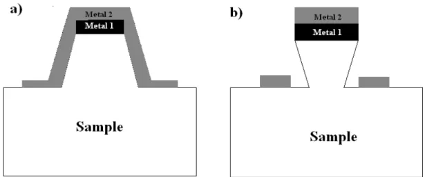
that base etching is preferred to be low damage and the etching profile should have negative slope so that the self-aligned structure can be obtained without shorting the emitter and base as shown in Figure 4.2.
Figure 4.2: Self-aligned metallization on a)positive and b)negative slope etched surfaces
The BPECO/DI etching was performed at 20 V for 2x60 minutes to etch 200 nm GaN emitter layer. After 60 minute oxidation, the grown oxide was etched in HCl and then another 20 V 60 minute oxidation was performed to etch 200 nm emitter layer.
4.2.4
Metallization
The metallization is a step to make ohmic or Schottky contacts to the desired regions defined by photolithography step. For this process, the metals were evaporated by using ultra high vacuum LE590 boxcoater. All the metallization processes were done under vacuum less than 5x10⁻⁶ mBar. The metallization
step is also very critical to make good ohmic and Schottky contacts, therefore the samples were dipped into HCl/DI (1:2) solution right before loading to vacuum chamber to remove the native oxide on the surface. As a result, contact quality
4.2.5
Annealing
The contacts were annealed by using rapid thermal annealing (RTA) system to have better ohmic contacts on n- and p-type materials. The ohmic contacts deposited were annealed at 750◦C under nitrogen and 550◦C under air for n- and
p-types, respectively. Also annealing is very critical before BPECO/DI oxidation because non-annealed metals and metals annealed at temperatures higher than 750 ◦C or lower than 650 ◦C were oxidized during BPECO/DI etching and they
were removed in HCl bath. However, if the metals were annealed at 680◦C, they
were not affected by BPECO/DI etching and they were not removed during HCl bath.
4.3
Bipolar Transistor Fabrication Process
The bipolar transistor fabrication is a 10 step process and the device structure given in Figure 4.3. Also a scanning electron microscope (SEM) image of the device before planarization can be seen in Figure 4.5.
4.3.1
Activation Annealing
During MOCVD growth, magnesium (Mg) in the p-type material is deactivated by hydrogen (H) atoms. A high temperature annealing was required to activate Mg atoms. Hence the samples were annealed at 750◦C for 60 minutes. The
ac-tivation temperature was kept high enough so that the acac-tivation was completed and low enough so that the GaN crystal structure was not deformed and the Mg diffusion to n-type layers were avoided. The activation time was usually between 15-30 minutes if p-type materials at the top most layer but in npn structure,
Figure 4.3: Bipolar junction transistor device structure
there is a 200nm emitter layer on the base and its duration was increased to 60 minutes to increase the outdiffusion of H atoms.
4.3.2
Emitter Contact
The emitter contact was patterned by a normal photolithography and then Ti/Al/Ni/Au (200 A◦/1500 A◦/800 A◦/6000 A◦) was evaporated. The total
metal thickness was approximately 850 nm. Since the contact hills to RF pads were defined at this step, the thick emitter metal made the planarization easier and reliable. Then the metal was annealed to increase ohmic quality and not to be oxidized in the next BPECO/DI etching process. The emitter metal after annealing is seen in Figure 4.4.
Figure 4.4: The emitter metal after annealing
4.3.3
Base Etch
Before base etching by BPECO/DI etching, a 200nm SixNy layer region was
patterned by photolithography, and SixNy was grown by PECVD and then
lift-off. This SixNy layer protected some unused parts on the sample so that
the BPECO/DI etch depth was measured. After SixNy growth, the layer was
BPECO/DI oxidized at 20 V for 60 minutes and the oxide was removed by HCl bath. Then the etch depth was measured from SixNy features on the sample.
The etch depth was usually in the range of 90-120 nm. Therefore to etch total of 200nm, once BPECO/DI oxidation was done at 20 V for 60 minutes and the oxide was removed by HCl bath. Finally, the SixNy layer was removed in a
4.3.4
Base Contact
After base etching, base PL was done and Ni/Au (100 A◦/200 A◦) metallization
was used to have ohmic contact to p-type GaN material. After lift-off, the metal was annealed at 550oC for 180 seconds under air to make ohmic contact.
4.3.5
Collector Etch
The collector contact should be on the highly doped subcollector region so that a good ohmic contact was done to collector region. Therefore the base and unintentionally doped (UID) collector layers were needed to be etched. With an image reverse lithography of base, it was etched down to subcollector region via RIE etching.
4.3.6
Collector Contact
After collector contact PL, Ti/Al/Ni/Au (200 A◦/1500 A◦/400 A◦/500 A◦) was
evaporated. The collector contact was not annealed but since it was made on a highly doped n region, it showed good ohmic quality.
4.3.7
Mesa Isolation
The devices on the sample and more importantly the base hill and subcollector region should be isolated. For this reason, mesa PL was done and etched down to the middle of the undoped buffer layer.
4.3.8
Post Formation
Post between the base hill and base metal was required before bridge metalliza-tion because the bridge would go over this post. The post material was a polymer PMGI. PMGI is widely used for this purpose, because of its desired reflow prop-erties and its suitable chemistry to the normal PL. After PMGI spinned, post PL was done and then it was exposed under 200 W UV source. After exposure, PMGI was developed in developer MF319/DI (1:1) and the photoresist was re-moved with acetone. Finally, the post was baked to reflow. The reflow is needed to provide a smooth and continuous way for the bridge or to prevent breaking the bridge from edges.
4.3.9
Air Bridge Process
After post reflow, bridge metallization PL was done and Ti/Au (300 A◦/8000
A◦) was evaporated. The bridge metal should be thick enough to increase its
endurance. The SEM picture of the device after air bridge formation is given in Figure 4.5.
4.3.10
Planarization
The planarizaion is required for RF pad metal formation. We have used benzo-cyclobutene (BCB) for planarization. After hard bake, BCB is very resistive to chemicals and has a very high resistance (1x10¹⁹Ωcm), hence it is widely used
for this purpose. After spinning BCB and hard baking, by RIE etching with
CHF3 and O2 gas mixture, BCB was etched below the level of emitter, base and
collector hills. It has to be noted that BCB etching is very critical. Etching less than the required level, would make open all the contacts and etching more would short the emitter base contacts. Hence the emitter metal was evaporated
thick (850nm) to prevent shorting emitter base contacts. Together with emitter region thickness (200nm), there was a 1 µm safe region to stop etching.
4.3.11
RF Pad Metal Formation
After planarization, the RF pad metal PL was done and Ti/Au (300 A◦/6000
A◦) was evaporated. Thick metal pads decrease the parasitic resistances and
increase the device performance. The RF pad metal formation was the last step of fabrication and final view of the device pictures taken by optical microscope is given in Figure 4.6.
Figure 4.5: The device after air bridge process (top) and the air bridge connecting the base to the base hill (bottom)
Chapter 5
Measurements and Results
5.1
Schottky Measurements and Results
The current-voltage characteristics of Schottky contacts fabricated on surfaces with various treatments are summarized in Table 5.1. The estimated breakdown voltage was calculated assuming uniform field in the undoped GaN.
Voltage (V) Time (min) Etch Depth (nm) Post Etch Treatment Breakdown Voltage (VBR (V)) Ideality Factor Estimated Break-down Voltage VBR (V) - - 0 - -70 1.25 -70 4 60 50 - -54 1.52 -63 4 60 50 annealed -60 1.89 -63 6 60 65 - -44 1.71 -61 6 60 65 annealed -51 1.72 -61 6 120 130 - -33 1.67 -52 6 120 130 annealed -41 1.82 -52 8 60 120 - -38 1.93 -52 8 60 120 annealed -54 1.97 -52
Table 5.1: Characteristics of Schottky contacts fabricated on GaN surfaces with various treatments.
−70 −60 −50 −40 −30 −20 −10 0 −10−3 −10−4 −10−5 −10−6 −10−7 −10−8 −10−9 −10−10 −10−11
Scottky I−V Curve
Current(A) Voltage(V) Not damaged 4V 60min 4−60 anneal 8V 60min 8−60 anneal 6V 60min 6−60 anneal 6V 120min 6−120 anneal
Figure 5.1: Reverse current-voltage characteristics of Schottky contacts fabri-cated on surfaces after various treatments.
0 0.1 0.2 0.3 0.4 0.5 0.6 0.7 0.8 0.9 1 10−11 10−10 10−9 10−8 10−7 10−6 10−5
Scottky I−V Curve
Current(A) Voltage(V) Not damaged 4V 60min 4−60 anneal 8V 60min 8−60 anneal 6V 60min 6−60 anneal 6V 120min 6−120 anneal
Figure 5.1 and 5.2 show the reverse and forward current characteristics of these devices. From these results, we saw that the BPECO/DI etching results in a reduction in breakdown voltage and an increase in the ideality factor. The breakdown voltages were higher for samples that have been annealed after the removal of the BPECO/DI oxide. After annealing, under certain conditions, breakdown voltages increased back to a value that was expected from the decrease in the undoped layer thickness. Thus, it was demonstrated that by etching of BPECO/DI oxide and subsequent annealing it is possible to fabricate good quality Schottky diodes on surfaces etched as much as 120 nm. Thus, it can be suggested that after the oxidation, etching, and annealing procedures the surface obtained is low damage.
The capacitance-voltage (C-V) characteristics presented in Figure 5.3.a-c in-dicated that all diodes were fully depleted at reverse biases and the untreated surface had uniform carrier density profile. After etching of the PEC grown oxide, the surface had a region of low carrier density as indicated by the high slope observed in Figure 5.3.b for bias voltages close to 0 V. After annealing, the C-V characteristics shown in Figure 5.3.c approached to that of an untreated surface shown in Figure 5.3.a. Given the information about the point defects in GaN [33, 34], it may be concluded that the defects created by bias assisted PEC oxidation are gallium vacancies bound to oxygen interstitials. Previous stud-ies based on photoluminescence investigation of GaN etched by PEC in KOH solution have reached the same conclusion [35].
AFM scans indicated a roughening of the etched surfaces after oxidation. The mean roughness of the as grown sample was 0.3 nm. As measured from a sample that was oxidized for 2 hours with 6 V bias, the root mean square (RMS) roughness of the etched surfaces was 15.6 nm and the mean RMS roughness of the etched surfaces after annealing was 10.3 nm. The increased roughness of the
Figure 5.3: The 1/C2 as a function of bias for a Schottky structure a) on
un-treated surface b) on surface etched by PEC oxidation at 6 V for 120 minute c) on surface etched as in b) and annealed as described in the text.
etched surface indicated that the oxidation process was not diffusion limited de-spite the presence of an oxide cover. This indicated that our process of oxidation likely had some deficiencies manifesting itself in the nonsaturating etch depths and the increase in roughness. It was also possible that the increased roughness was related to the defects in the material being etched [36].
The fact that near ideal breakdown voltages and C-V characteristics were obtained on 120 nm etched surfaces after a 700 oC 30 s anneal indicated that
In contrast, surfaces etched by RIE by only 10 nm using the best techniques requires a 850 oC, 30 s anneal for damage removal. Deeper RIE etches requires
etching of the sample by KOH for damage removal, making the process unusable for practical purposes. Similarly, the PEC process is not suitable for use in self-aligned emitter-base etching GaN HBT structures, since PEC employs KOH during the etching process which needs to be performed at low etching rates to achieve low damage. Thus, etching of GaN by etching of BPECO/DI oxide stands out as a unique tool for deep etching without creating extensive surface damage. Such a process is critically needed for GaN based HBT fabrication.
The reduction of the roughness after annealing might be a factor in the im-provement of the Schottky characteristics seen with annealing. However, the C-V and AES results showed that the improvement was more likely to be related to removal of point defects. The reduction of the RMS roughness observed with the annealing may be attributed to decomposing of the oxide that remains on the surface after oxide etching. However, no change in oxygen ratio was observed with AES. So, the mechanism with which the annealing resulted in smoothing of the etched surface remained unclear.
We have demonstrated good quality Schottky contacts on surfaces etched 120 nm using the BPECO/DI process. These results presented here are the first experiments reporting a good quality Schottky devices on GaN surfaces etched more than a few tens of nanometers by any method. The good quality of the Schottky contacts indicated that low-damage etching of GaN surfaces could be achieved by BPECO/DI process. Annealing of the etched surfaces at 700 oC for 30 seconds in nitrogen resulted in successful removal of the etch
damage. After this anneal, the Schottky breakdown voltages approached to the values expected from the reduced thickness of the n-GaN layer. Capacitance-voltage measurements indicated the reduction in Schottky breakdown Capacitance-voltages after etching and the improvement observed after annealing was most likely due
Figure 5.4: I-V characteristics of 7µm TLM pattern on control, BPECO/DI etched and RIE etched surfaces
to point defects. The roughening that resulted from the BPECO/DI oxidation and etching was not clearly understood and was likely to be related to deficiencies in our specific equipment and should be investigated further on.
In addition to Schottky contact study, p-type and n-type ohmic contacts were formed on BPECO/DI etched surfaces. From the measured n-type ohmic contacts, no difference was observed between the I-V characteristics of TLM patterns on etched surface and unetched surface. However for the p type contacts, the measured I-V characteristics degraded with BPECO/DI etching but it was much better than the I-V characteristics of the contact on the RIE etched p-type.
The changes in Schottky diode characteristics and ohmic characteristics sug-gest that the BPECO/DI etching results in a damage near surface. Improvement of reverse characteristics and nearly unchanged ideality factors support that some of the damage can be improved and some cannot be removed by short annealing.
An explanation for the observed Schottky characteristics and ohmic behaviors can be that BPECO/DI etching creates defects on or close to surface. These states cause trap assisted tunnelling and degrade reverse leakage as explained in Chapter 2. Annealing removes these states and therefore passivation of surface states improves reverse characteristics. Also compensating defects very near to surface decrease the free carrier density near the surface by capturing electrons. This was observed in C-V measurements and it got close to the original case after annealing out the near surface states. This defect can be gallium vacancies bound to oxygen interstitials VGa− ON, because during oxidation, OH− ions
prefer to make chemical reactions with gallium (Ga) atoms instead of nitrogen (N) atoms. This fact and presence of oxygen (O) atoms increase the density of gallium vacancies VGa. Hence a consistent picture is that there are gallium
vacancies VGaand gallium vacancies bound to oxygen interstitials VGa−ON, that
is, gallium vacancy-oxygen complexes [33, 34]. This defect was also observed in PEC etched surfaces as the origin of yellow luminescence [35]. Since these defects are compensating, the degradation in p-type ohmic quality can also be explained by decreased hole concentration on the p-type surface.
The change in ideality factor of Schottky diodes might be explained by nonuniform Schottky barrier height (NSBH) explanation of Tung [18]. It is known that the Schottky barrier height is nonuniform for inhomogeneous sur-faces. This inhomogeneity can be due to the nonuniform etching, surface rough-ness due to nonuniformity sources coming from the etching system like light intensity, potential distribution, etc. As a result of this nonuniformity, there are patches with different SBH’s and the current conduction occurs through these patches. This conduction mechanism is called ”parallel conduction mechanism” and a sum of individual currents flowing through the patches with area (Ai) and
SBH (φi) is given by; I =X i Ii = A∗T2[exp(βVa) − 1] X i exp(−βφi)Ai (5.1)
Tung claims that ”The parallel conduction mechanism is in significant error when the SBH varies spatially on a scale less than, or comparable to, the depletion region width. The error arises because the equation fails to take into account the interaction between neighboring patches with different SBH’s.” The situation can be explained by the conduction path through a low SBH patch with neighbor high SBH patches is pinched off. The pinch off is defined as majority carriers see a barrier higher than the band-edge at metal-semiconductor interface. This pinch off results in deficiencies in ideality factor.
The being pinched off for a patch is directly related to its size. The potential distribution by solving the Poission equation gives that the potential increases up to a distance then it decreases along the patch, if the patch size is less than the peak point position, then the patch is pinched off due to the potential distribution electrons see a higher barrier than the band edge barrier. This condition is given by the equation:
∆
Vbb
> 2R0
W (5.2)
where ∆ is the barrier height difference between low SBH and neighbor SBH’s,
Vbb is the band banding potential, R0 is the radius of the patch, and W is the
depletion width.
As it is mentioned, the patch sizes less than or comparable to depletion width are pinched off. Since the doping of semiconductor controls the depletion width, the number of pinched off patches are directly related to the doping of semicon-ductor. After knowing the potential distribution, the current flowing to and from low SBH patches can be calculated.
n = 1 + γ
3η1/3V2/3
bb
(5.3)
where η ≡ ²s
qND and the patch size characteristics γ is defined as γ ≡ 3(∆R
2 0/4)1/3
Then an ideality factor can be calculated from dI/dV and it is given in Equa-tion (5.3). This also explains the doping and applied potential dependence of the ideality factor and enlightens the anomaly on the ideality factor.
Explanations given above can enlighten the measurement results. Although we have used all available measurement instruments to investigate the etching damage, temperature dependent measurements and deep level transient spec-troscopy (DLTS) can be done for further understanding of the damage mecha-nism of BPECO/DI etching.
5.2
Bipolar Transistor Measurements and
Re-sults
The fabricated devices, as explained in Chapter 4, were measured on HP 4145B. The I-V characteristics of TLM patterns on all regions, emitter and base-collector junctions were measured to characterize the device performance.
After etching the emitter layer and forming the self-aligned base contact, the current-voltage characteristics of TLM patterns on base region were measured. The I-V characteristic of a 6 µm TLM pattern of 40x100 µm is shown in Figure 5.5. In addition to the high base resistance, a rectifying voltage of 5V for nonan-nealed base contact and 2 V for annonan-nealed base contact were observed in the base TLM measurements. These nonidealities, the high base resistance and rectifying voltage, are mainly due to the low doping concentration in the base and poor base contacts. A similar rectifying, 2 V, voltage can also be seen in Figure 5.4, the I-V characteristics of TLM pattern on bare p-type material and it could be deduced that it would be much worse if RIE etched.
I-V characteristics of base-emitter junction and base-collector junction were shown in Figure 5.6 and Figure 5.7. Figure 5.6 demonstrates that self aligned base-emitter junction was not shorted and diode characteristics proved that the base metal was on p-type layer. In order to further determine the base con-tact placement, two experiments were performed. We have intentionally etched one sample less than emitter thickness and another sample more than total of emitter and base thicknesses. In other words, base metals were placed on emit-ter and collector layers. Both I-V measurements showed back-to-back Schottky characteristics. Figure 5.8 shows I-V characteristics of TLM patterns on sample intentionally etched less than emitter thickness. Therefore it was sure that in our experiment, we achieved to place the base metal on the p-type layer.
The ideality factor and breakdown voltage of base-emitter junction were in the range of 2-3.5 and 14-22 V respectively. On the other hand, the ideality factor and breakdown voltage of base-collector junction were between 4-5.5 and 50-75 V respectively. High ideality factors for GaN based p-n junctions have commonly been seen because of low doped base region. Furthermore high ideality factor of base-collector junction could be related to the low doping of collector region.
Figure 5.6: I-V Characteristics of base-emitter junction in linear scale (top) and logarithmic scale (bottom)
Figure 5.7: I-V Characteristics of base-collector junction in linear scale (top) and logarithmic scale (bottom)
Figure 5.8: I-V Characteristics of TLM patterns on sample intentionally etched less than emitter thickness in linear scale (top) and logarithmic scale (bottom)
doping of emitter and thin base layer. The effect of high base resistance is also effective on both the degradation of ideality factors and the low current densities in both junctions. Due to high access base resistance, the current density in base-emitter junction was too low because base-emitter junction is affected by access base resistance much more than base-collector junction.
Chapter 6
Discussions and Conclusions
The lack of a low damage etching process that is compatible with rest of the fabrication steps has been a factor hindering GaN HBT fabrication. For the fabrication of GaN HBTs, an n/p doping selective etch process that does not result in damaged surfaces after 100 to 150 nm etching is necessary.
In this study, we demonstrated that BPECO/DI etching yields low-damage surfaces after etching as much as 120 nanometers. A post-etch anneal at 700
oC is required to improve the surface characteristics to near ideal. The
prop-erties of surfaces oxidized and etched by BPECO/DI were investigated using Schottky diodes fabricated on etched surfaces and also by using Auger electron spectroscopy (AES) and atomic force microscope (AFM) measurements. The results presented here should motivate further investigation of BPECO/DI for use in GaN HBT processing.
Then we have fabricated self aligned bipolar transistors by engineering BPECO/DI etching. The fabricated devices did not work as estimated. The reasons that degrade the transistor performance can be base material quality as-sociated with growth or fabrication. First of all, the fabricated p-type layer with the similar conditions of p-type material of npn layers has shown 1 Ωcm sheet
resistance and this is comparable to the p-type sheet resistances in the literature. However, the p-type surface was always very rough compared to n-type materials and hexagonal shaped defects were intensively seen on the surface.
On the other hand, the problems might come from fabrication. First of all, the activation annealing has to be done before emitter etch because the emitter contact cannot stand for long and high temperature activation annealing. Furthermore since there is undercut, the mushroom like emitter structure melts and the emitter-base junction shorts. Hence while activating p-type base, there is a 200nm emitter layer on the base. This might prevent the outdiffusion of the H atoms that inactivate the Mg atoms in p region.
There are also some uncertainties with BPECO/DI etching. For instance, the roughening mechanism still cannot be understood fully. The reason of roughening in PEC etching is proposed to be dislocations and this can be overcome by increasing the UV light intensity or decreasing the concentration of electrolyte. However, we could not achieve smooth surface as in PEC etching. Also while etching npn layers, the etch rates were decreased and surface roughness was significantly increased compared to n layers etched with the same conditions. This can be explained by the reduction of hole lifetime in highly doped emitter layer. Also the high defect and dislocation density in p-type region affect n+ emitter region grown afterwards. Hence this also explains that the etch rate of n+ emitter layer decreases and the surface roughness increases.
The future study can be focused on npn layer growth and also on HBT fabrication by utilizing BPECO/DI etching. Even though currently there are still problems that should be solved for good bipolar transistor characteristics, this fabrication method is a very strong candidate for the future GaN bipolar transistor fabrication.
Bibliography
[1] S. Nakamura and S. Chichibu, Nitride Semiconductor Blue Lasers and Light
Emitting Diodes. Taylor and Francis. 352, 2000.
[2] Y. Wu, A. Saxler, M. Moore, R. Smith, S. Sheppard, P. Chavarkar, T. Wisleder, U. Mishra, and P. Parikh, “30-w/mm gan hemts by field plate optimization,” IEEE Electron Device Letters, vol. 25, no. 3, pp. 117–119, 2004.
[3] J. Lee, V. Kumar, R. Schwindt, A. Kuliev, R. Birkhahn, D. Gotthold, S. Guo, B. Albert, and I. Adesida, “Microwave noise performances of al-gan/gan hemts on semi-insulating 6-h sic substrates,” Electronic Letters, vol. 40, no. 1, pp. 80–81, 2004.
[4] B. Green, V. Tilak, S. Lee, H. Kim, J. Smart, K. Webb, J. Shealy, and L. Eastman, “High-power broad-band algan/gan hemt mmics on sic sub-strates,” IEEE Transactions on Microwave Theory and Techniques, vol. 49, no. 12, pp. 2486–2493, 2001.
[5] V. Bougrov, M. Levinshtein, S. Rumyantsev, and A. Zubrilov, Properties of
Advanced Semiconductor Materials GaN, AlN, InN, BN, SiC, SiGe. John
Wiley and Sons Inc., New York, 2001.
[6] M. Farahmand, C. Garetto, E. Bellotti, K. Brennan, M. Goano, E. Ghillino, G. Ghione, J. Albrecht, and P. Ruden, “Monte carlo simulations of electron