STRUCTURES IN PHOTONIC CRYSTALS
Ekmel Ozbay and Mehmet Bayindir Department of Physics, Bilkent University Bilkent, 06533 Ankara, Turkey
Abstract We propose and demonstrate a new type of propagation mechanism for electro-magnetic waves in photonic band gap materials. Photons propagate through cou-pled cavities due to interaction between the highly localized neighboring cavity modes. We report a novel waveguide, which we called coupled-cavity waveguide (CCW), in three-dimensional photonic structures. By using CCWs, we demon-strate lossless and reflectionless waveguide bends, efficient power splitters, and photonic switches. We also experimentally observe the splitting of eigenmodes in coupled-cavities and formation of defect band due to interaction between the cavity modes. The tight-binding (TB) approach, which is originally develop for the electronic structures, is applied to the photonic structures, and compared to the experimental results. Our achievements open a new research area, namely physics and applications of coupled-cavities, in photonic structures. We think that our results are very important for constructing future all-optical components on a single chip.
1.
Introduction
The artificially created 3-dimensional (3D) periodic structures inhibit the propagation of electromagnetic (EM) waves in a certain range of frequencies in all directions [1, 2]. In analogy with electronic band gaps in semiconduc-tors, these structures are called photonic band gap (PBG) materials or photonic crystals[3, 4]. The initial interest in this area came from the proposal to use PBG crystals to control spontaneous emission in photonic devices[1]. How-ever, the technological challenges restricted the experimental demonstrations and relevant applications of these crystals to millimeter wave and microwave frequencies[5, 6]. Recently, Fleming and Lin reported a photonic crystal with a band gap at optical frequencies[7, 8]. With this breakthrough, initially pro-posed applications like thresholdless semiconductor lasers[9] and single-mode light-emitting diodes[lO] became feasible.
273
A.S. Shumovsky andv.1.Rupasov (eds.), Quantum Communication and Information Technologies, 273-297.
Localized Cavity Modes
A Overlapping Cavity
Regions
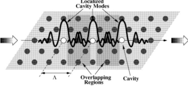
Figure1. Schematics of a coupled-cavity (white circles) structure in a two-dimensional pho-tonic crystal (black circles). Tightly confined cavity mode interacts weakly with the neighboring cavity modes, and therefore the electromagnetic waves can propagate through coupled cavities.
Analogy between the Schrodinger equation and Maxwell's equations allows us to use many important tools which were originally developed for the elec-tronic systems. As an example, it is well known that the TB method has proven to be very useful to study the electronic properties of solids[1l]. Recently, the classical wave analog of the TB picture[12] has successfully been applied to the photonic structures[13, 14, 15, 16, 17, 18]. Sterke investigated the proper-ties of the one-dimensional optical superlattices within the TB approximation [13]. Lidorikis et al. obtained matrix elements of the TB Hamiltonian for two-dimensional photonic crystals, with and without defects, and tested the TB model by comparing it to the corresponding ab initio results[15]. Observation of the normal mode splitting in quartz polystyrene was well explained by the TB photon approach[16].
By using direct implications of the TB picture, a novel propagation mecha-nism for photons along localized coupled cavity modes in photonic crystals was theoretically proposed[14, 17], and experimentally demonstrated[18]. In these structures, photons can hop from one tightly confined mode to the neighboring one due to the weak interaction between them (See Fig. 1). Stefanou and Modinos obtained the cosine-like dispersion relation for their coupled-defect waveguides and waveguide bends with and without disorder[14]. Later, Yariv et al. reformulated the same phenomenon in a simple way, and more importantly proposed various applications based on coupled-cavity structures[17].
In the last few years, we proposed and demonstrated various applications based on coupled-cavity structures in photonic crystals. We experimentally ob-served the eigenmode splitting, and explained by using the TB picture [18,19]. Guiding and bending of EM wave [20], heavy photons [21], and EM-beam splitting and switching effect [22] were experimentally demonstrated in three-dimensional photonic crystals at microwave frequencies. We also reported
ob-servation of directional coupling in coupled photonic crystal waveguides [23], and dropping of photons via cavity and waveguide coupling [24, 25]. In addi-tion, we investigated one-dimensional (10) coupled optical microcavity (CMC) structures [26, 27], and observed the strong enhancement of spontaneous emis-sion throughout the cavity band in such structures [28].
Very recently, the coupled-cavity structures in photonic band gap materials have inspired considerable attentions [29,30,31,32,33,34]. For instance, Lan
et
at.
numerically proposed a switching mechanism by changing the positions of the sharp edges of the coupled-cavity band of 10 PBG structures [31], and delay lines for ultrashort optical pulses [32, 33]. Olivier et al. reported 20 CCWs at optical wavelengths [29]. The coupled-mode theory is applied to the coupled-cavity structure by Reynolds and his co-workers [30].2.
Localized Coupled-Cavity Modes in Photonic Crystals
In this section, we give a detail analysis of the TB picture in photonic band gap structures. We first investigate splitting of eigenmodes of coupled cavities, photonic molecules, by using the TB approach [18]. Then, we derive simple expressions for physical quantities such as dispersion relation, group velocity, photon lifetime, and dispersion.
Consider a strongly localized modeEo (r) corresponding to a single cavity that satisfies simplified version of the Maxwell equations
\7 x [\7 x Eo(r)]
=
Eo(r)(Ojc)2Eo(r) , (1)(2)
where EO(r) is the dielectric constant of the single cavity, 0 is the frequency
corresponding cavity mode, and c is the speed of light. In order to derive the foregoing equations, we assumed that Eo (r) is real, nondegenerate and orthonormal:
J
drEo(r)Eo(r) . Eo(r) = 1 .2.1
Photonic molecules: eigenmode splitting
When two localized cavity modes are brought in contact, the corresponding eigenmode can be obtained from superposition of the individual evanescent cavity modes
Ew(r)
=
AEo(r)+
BEo(r
- Ai:) .
(3)The eigenmodeEw(r) also satisfies Eq. (1) whereEo(r) is replaced with the dielectric constant of the coupled systemE(r)
=
E(r -Ai:),
and 0 is replaced with eigenfrequency w of the coupled cavity mode.Inserting Ew(r) into Eq.(1),and multiplying both sides from the left first by ES/ (r) and then by ES/ (r -
Ax)
and spatially integrating the resulting equations, we obtain the splittingwhere0:1 and(31 are the first order coupling parameters which are given by
0:1
=
J
drE(r)ES/(r) . ES/(r -Ax) ,
and
(31 =
J
drEo(r -Ax)ES/(r)
.
ES/(r -Ax) .
Corresponding photonic modes are given by
( )_ ES/(r)
±
ES/(r -Ax)
EW12
,
r -y2
m '(4)
(5)
(6)
(7)
From Eq. 4, we observe that the single cavity mode splits into two distinct photonic modes due to interaction between the cavities. This splitting is anal-ogous to the splitting in the diatomic molecules, for example
Ht,
in which the interaction between the two atoms produce a splitting of the degenerate atomic levels into bonding and antibonding orbitals[12]. Recently, the bond-ing/antibonding mechanism in a photonic crystal was theoretically proposed by Antonoyiannakis and Pendry [35, 36]. The splitting phenomenon was experi-mentally observed in quartz polystyrene[16] and in photonic molecules[37].Similarly, in the case ofthree coupled-cavities, the eigenmode can be written as
Ew(r) =
AES/(r)
+
BES/(r
- Ax)
+
CES/(r -2Ax)
.
(8)In this case, the single cavity mode splits into three distinct modes which are given by
where 0:2 and (32 are the second nearest neighbor coupling terms which are given by
and
0:2 =
J
drE(r)Eo(r) . Eo(r -
2Ax) , (10)(32 =
J
drEo(r -
2Ax)Eo(r) .Eo(r -
2Ax) . (11)After finding the coefficients in Eg. 8, the corresponding eigenmodes are given by
E
()
=Eo(r)
±
V2
E o(r -
Ax)+
Eo(r -
2Ax)r
1,3r
2 '()
Eo(r) - Eo(r -
2Ax)Er2 r
=V2
2.2
A novel waveguiding mechanism
(12)
(13)
When we consider an array of cavities in which each cavity interacts weakly with neighboring cavities, a defect band1is formed (See Fig. 1). The eigenmode
of this waveguiding band can be written as a superposition of the individual cavity modes which is analogous to the linear combination of atomic orbitals in solid state physics[II]:
E(r)
= EoL
e-inkAEo(r -
nAx) ,n
(14)
where the summation overnincludes all the cavities, andk is the wavevector. The dispersion relation for this structure can be obtained from Egs. (1) and (14) keeping only the first two coupling terms
w(k) =
n
((31 cos(kA)+
2(32 cos(2kA)+
1/2) 1/2 (15) 0:1 cos(kA)+
20:2 cos(2kA)+
1/22.3
Dispersion relation and group velocity
In certain cases, we can safely ignore the second nearest neighbor terms, and this approximation leads to a simpler expression for the dispersion relation
w(k)
=
D [1+
K;cos(kA)] . (16)Here K;
=
(31 - 0:1 is a TB parameter which can be obtained from the splittingof the eigenmodes of two coupled cavities. After obtaining D,WI,andW2from measurements or simulations, one can determine (31 and 0:1 values by using
Eq. 4. The bandwidth of the waveguiding band is proportional to the coupling constant and single cavity frequency, which is given by
(17)
Group velocity of photons along the coupled cavities can be determined from the dispersion relation as
or the group velocity as a function of frequency is given by
(
2) 1/2
vg(w)=AD
K;2_(~-1)
.
(18)
(19)
Figure 2 displays the calculated dispersion relation and the group velocity as a function of frequency w. Due to flat dispersion, the group velocity vanishes at the band edges, i. e., k
=
0 and k=
7r /A. This property can be used invarious applications. For instance, the efficiency of nonlinear processes can be enhanced due to small group velocity at the band edges [17, 38].
2.4
Photon lifetime and dispersion
The net phase differenceL:1<p is related with the wave vector k of the crystal
kL - koL = L:1<p , (20)
where L is the total crystal thickness, ko = 27rw/c, and c is the speed of the light in vacuum. Combining Eqs. (16) and (20) along with the definition of Tp
=
o(
L:1<p) /OW,
we obtain a formula for delay time, photon lifetime, as a function of frequency1.0 0.05 (b) 0.04 0.03 ~ ;;.co0.02 0.01 0.00 1.0 0.0 0.5 kA/n 0.5 kA/n (a) 1.10 r----,....---, 0.95 0.90 L...- ' - -_ _----' 0.0 1.05 ~ 1.00 8
Figure 2. Calculated (a) dispersion relation and (b) group velocity as a function of wavevector kfor parameterIi, = -0.05, A = 2em,and0 = 10 GHz. vg tends towards to zero at band
edges k =
a
and1r /A.(21) The dispersion is given by
D(w) _
~ (~)
_~
dTp _ win - 1- dw vg - L dw - An2
(K;2
_
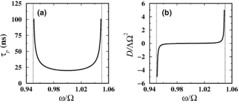
(win _ 1)2)3/2 (22)We calculated the photon lifetime by using Eq.21, and plotted in Fig. 3(a). The photon lifetime goes to the infinity at the band edges, i. e., w
=
(1
+
K;)nand w
=
(1 -
K;)n. This means that photons move along the coupled cavities very slowly, and therefore we can introduce theheavy photon concept in such photonic structures. The heavy photons at the coupled-cavity band edges are analogous to the electrons in semiconductors having energies near the band edges [12].We also calculated the dispersion D as a function of normalized frequency
win. As shown in in Fig. 3(b), we observed thatD --+ -00forw =
(1
+
K;)n andD --+ +00forw=(1 - K;)
n.
Based on this important observation, we canuse the coupled-cavity structures as dispersion compensators.
3.
Coupled-Cavities in 3D Photonic Crystals
In this section, we investigate experimentally and theoretically the coupling between localized cavity modes in a dielectric-based layer-by-layer 3D photonic crystal within the TB framework. We also report on the observation of the
125 6 (a) 4 (b) 100 2 ,- 75 N
'"
c:
=
0 '-':;:
I' p"- 50 C::i -2 25 -4 0 -6 0.94 0.98 1.02 1.06 0.94 0.98 1.02 1.06 colO colOFigure3. Calculated (a) delay time and (b) dispersion as a function of normalized frequencyw.
The delay time increases rapidly as we approach to the waveguiding band edges. The dispersion goes to-00at the lower band edge and+00at the upper band edge.
eigenmode splitting in the coupled cavities. Moreover, we demonstrate a new type of waveguiding through localized defect modes.
3.1
3D layer-by-layer photonic crystals
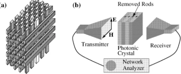
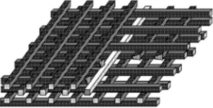
A layer-by-Iayer dielectric based photonic crystal [39,40, 7] was used to con-struct the coupled-cavity con-structures as shown in Fig. 4(a). The crystal consists of square shaped alumina rods having a refractive index 3.1 at the microwave frequencies and dimensions 0.32 cmxO.32 cmx 15.25 cm. A center-to-center separation between the rods of 1.12 cm was chosen to yield a dielectric fill-ing ratio ofrv 0.26. The unit cell consists of 4 layers having the symmetry of
a face centered tetragonal (fct) crystal structure. The crystal exhibits a three dimensional photonic band gap extending from 10.6 to 12.8 GHz.
The experimental set-up consists of a HP 8510C network analyzer and mi-crowave horn antennas to measure the amplitude and transmission-phase spectra [Fig. 4(b)]. The defects were formed by removing a single rod from each unit cell of the crystal. Removing a single rod from an otherwise perfect crystal leads to confined modes with high Q-factors, quality factor de-fined as the center frequency divided by the full width at half maximum, around 1000. The electric field polarization polarization vector of the incident EM field was parallel to the rods of the defect lines for all measurements.
3.2
Mode splitting
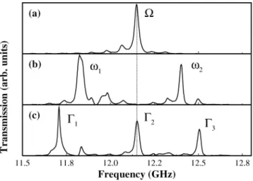
By using the aforementioned experimental setup, we first measured the trans-mission amplitude through a crystal with a single defective unit cell. This re-sulted in a localized defect mode within the PBG which is analogous to acceptor
Figure4. (a) Schematic drawing of the coupled-cavity structures in a layer-by-Iayer photonic crystal. A single rod (white rods) removed from each unit cell. (b) The experimental setup for measuring the transmission characteristics of the coupled-cavity structures in three-dimensional photonic crystals. The electric field polarization is directed along the removed rods.
impurity state in semiconductor physics [41]. The defect mode occurred at a resonance frequency of
n
=
12.150GHz with a Q-factor (quality factor, de-fined as center frequency divided by the peak's full width at half-maximum) ofrv 1000 [Fig. Sea)].
Next, we measured the transmission through the crystal that contains two consecutive single rod removed unit cells. The intercavity distance for this structure was A= 1.28cm, which corresponds to single unit cell thickness in the stacking direction. We observed that the mode in the previous case splitted into two resonance modes at frequenciesWI = 11.831GHz andWI = 12.402
GHz [Fig. S(b)]. The TB parameters found to be K, = (3 - 0:= -0.047.
Figure S(c) shows the transmission characteristics of a crystal having three consecutive defective cells, where the resonant modes were observed at fre-quencies
r
1= 11.708GHz,r
2 = 12.153GHz andr
3=
12.506GHz. Measured [GHz] f 1 11.708 f 2 12.153 f 3 12.506 Calculated [GHz] 11.673 12.150 12.492Table1. The measured and calculated values of resonant frequencies for the crystal with three defective unit cells.
Table 1 compares the resonance frequencies, which were calculated by in-serting TB parameters0:1and(31into the Eq. (9), with the values obtained from
the experiment [Fig. S(c)]. The experimentally measured three splitted modes coincide well with the theoretically expected values. This excellent agreement shows that the classical wave analog of TB formalism is valid for our structure.
(a) Q ~
'"
-'c
=
(b) .Q r-~ '-'=
0'm
'"
(c)·s
r
3'"
=
~ r-Eo-< 11.5 11.8 12.0 12.2 12.5 12.8 Frequency (GHz)Figure5. Transmission characteristics along the stacking direction of the photonic crystal: (a) For single defect with resonance frequency fl. (b) For two consecutive defects resulting in two splitted modes at resonance frequenciesWI andW2with intercavity distance A= 1.28 cm.
(c) For three consecutive defects with resonance frequencies
r
l ,r
2 ,andr
3 .3.3
Waveguide and waveguide bends
In this section, we demonstrate the observation of guiding and bending of the EM wave through highly localized defect modes in a 3D photonic crystal. The most important feature of this new waveguides, which we called coupled-cavity waveguides (CCWc), is the possibility ofconstructing lossless and reflectionless bends. This ability has a crucial role to overcome the problem of guiding light around very sharp corners in the optical circuits.
The guiding or bending of EM waves through the localized defect modes via hopping is fundamentally different from previously proposed photonic crystal waveguides [42, 43, 6, 44]. Although, the structural imperfections such as misalignment of rods during the fabrication process affected the efficiency of the CCWs, we have observed nearly 100 percent transmission for various CCWs throughout the entire waveguiding band. Our observation differs from that of Linet at. [43] in which the unity bending efficiency2can be obtained only at
certain frequencies.
3.4
Transmission measurements
We first measured the transmission characteristics of a straight waveguide which consists of 11 unit cell fct crystal. The defect array was created by
2In this reference, the bending efficiency is obtained by normalizing the transmission spectrum through the bend to that of the straight waveguide.
(a)
...
II::::::::: I:::::::::: -+:i1"i1"i1"i1"i:---+ I:::::::::: I::::::::::...
::~~~::::: :~::~:::: ---+:i:::'l:I.~:-+::::::ril:: I::::::::::o
-40 -20 Zig-zag Waveguide -60 L..-.L...-_...,;.Llo.-..._ ..._ ...L-_ _----:'----_----'6:
'0'-' -40=
Straight .~ Waveguide ~ OI-+---+--+--+L--+--1---'=---1 ... (b)~
E
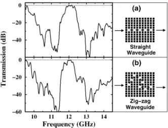
-20 Eo-10 11 12 13 14 Frequency (GHz)Figure6. (a) Transmission amplitude as a function of frequency for a straight waveguide geometry which is shown in the right panel. The gray squares represent the missing rods. A full transmission was observed throughout the entire waveguiding band ranging from 11.47 to 12.62 GHz. (b) Transmission characteristics of a zig-zag shaped waveguide which is formed by removing randomly chosen rods while keeping the distance between adjacent defects constant. In all cases, nearly 100 percent transmission amplitudes were measured.
removing a single rod from the first layer of each unit cell with a periodicity of A= 1.28 em. As shown in left panel of Fig. 6(a), a defect band (guiding band) was formed within the photonic band gap analogous to the impurity bands in the disordered semiconductors. The width of this guiding band can be adjusted by changing the coupling strength between the cavities3. For this waveguide structure, nearly a complete transmission of the EM wave was observed within a frequency range extending from 11.47 to 12.62 GHz. It is interesting to note that when we placed one of the removed rods into its original position, we observed almost vanishing transmission amplitude throughout the above frequency range. This result is expected since the second nearest-neighbor coupling amplitude is negligibly small in our structures.
To develop an optical circuit, the problem of the guiding light around sharp comers must be addressed. Conventional dielectric or metallic waveguides have large scattering losses when sharp bends are introduced. Within the TB approx-imation, we can guide or bend the EM waves along an arbitrarily shaped path by connecting the defects. To verify this idea experimentally, we constructed a zig-zag shaped waveguide while keeping the distance between the consecu-tive cavities constant. In this waveguide, the propagation direction of photons was randomly changed. As shown in Fig. 6(b), we observed full transmission
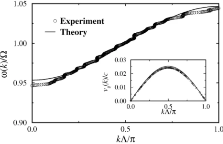
o Experiment - Theory 1.0 0.5 kA/rc 0.00 ¥:--~---'--~---'" 0.0 t.J 0.02 ~ ';:'~ 0.01 0.95 1.00 1.05 1.0 0.5 kNn 0.90 L...- ~ ---L.. ~ ~_ ______' 0.0
Figure7. Dispersion diagram of the waveguiding band predicted from the transmission-phase measurements (0 symbols) and calculated by using tight-binding formalism (solid line) with
K
=
-0.047. Inset: The normalized group velocity diagrams calculated by the theory (solidline) and obtained from the experimental data (0 symbols) agree well and both vanish at the guiding band edges, where c is the speed of light.
similar to the results obtained from the straight waveguide. Our results clearly indicate that the sharp corners have no influence on the propagation of EM waves in CCWs. By using CCWs one can achieve the bending of light around a sharp corner without any radiation losses. Therefore, this novel method may have great practical importance in certain applications.
As shown in Fig. 6, the band edges of CCWs are very sharp compared to the PBG edges. This property is important for the switching applications. Conventionally, the switching mechanism is achieved by dynamical shifting of the photonic band gap edges [45] or the position of defect frequency [46] via the nonlinear processes. In our case, the on-off modes of the switch can be achieved by shifting the waveguiding band edges. Therefore, the efficiency of a photonic crystal based switch can be enhanced by using the CCWs.
3.5
Phase measurements
The dispersion relation for the waveguiding band can be obtained from the transmission-phase measurement. Figure 7 shows the comparison of the mea-sured(0symbols) and calculated (solid line), by usingWk = 0[1
+
K,cos(kA)],dispersion relations. As shown in Fig 7., TB calculation gives good agreement with the measured result, and the deviations between the experiment and the theory is more pronounced around the edges of the waveguiding band. We ex-pect this discrepancy to vanish as the number of unit cells used in the experiment is increased.
35 0 Experiment - Theory 25 15 5 11.4 11.8 12.2 Frequency (GHz) 12.6
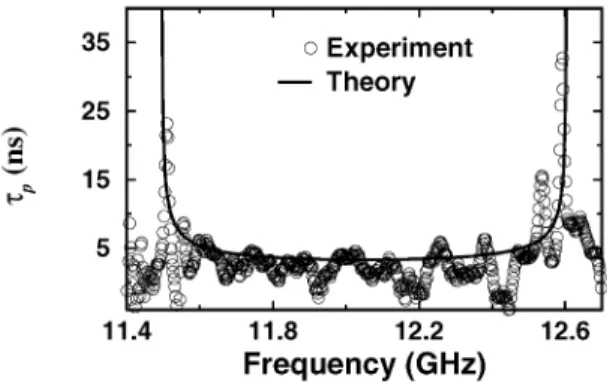
Figure 8. The measured and calculated delay time for the single rod removed CCw. The photon lifetime increases also drastically at the waveguiding band edges.
The inset in Fig. 7 shows the comparison of the theoretical (solid line) and experimental (0 symbols) variation of the group velocity,vg(k)
=
dw(k) /dk c:::: -DK;a sin (ka), of the waveguiding band as a function of wave vector k. The experimental curve is obtained by taking the derivative of the best fitted cosines function to the experimental data. Notice that the group velocity vanishes at the waveguiding band edges [47]. It is important to note that, in the stimu-lated emission process, the effective gain is inversely proportional to the group velocity [48]. The group velocity can be made smaller if one can reduce the amplitude of the parameterK;.3.6
Heavy photons at coupled-cavity band edges
Heavy photons or photons with a extremely low group velocity playa criti-cal role in enhancing the efficiency of nonlinear processes, [10, 48, 17] and the gain enhancement in the photonic band edge laser. [10] Moreover, the spon-taneous emission rate can be increased since the effective gain is proportional to l/vg . [48] The low group velocity was proposed near the band edges of one-dimensional photonic band-gap structures. [49, 10] Recently, Vlasov et al. have observed that the optical pulses significantly slow down at the 3D photonic crystal band edges in visible spectrum. [50]
We measured the delay time of a defect structure where the whole rod is removed from each unit cell of the crystal. [18] We measured the delay time corresponding to a ten unit cell coupled cavity waveguide. The localization volume is bigger than the previous case, and therefore the photon lifetime for a single cavity is around 5 ns. As shown in Fig. 8, the delay time increases drastically at the CCW band edges and agrees well with the calculated result by using Eg. (3). In this case, the group velocity also approaches to zero at the band edges (See the inset in Fig. 7).
Physically, the heavy photons in the photonic band gap structures are anal-ogous to the electrons in semiconductors having energies near the band edges. The corresponding eigenfunctions are standing waves rather than the running waves, and therefore the effective mass of electrons becomes very large. [12]
4.
Highly Confined Photonic Crystal Waveguides
Photonic crystals also provide a promising tool to control the flow of light in integrated optical devices [51,52]. Therefore, there is a great deal of interest in developing photonic crystal based waveguides where one can confine and efficiently guide the light around sharp corners in two-dimensional (20) [42, 43, 53, 54, 55, 56] or three-dimensional (3D) [6, 18, 57, 58, 59] photonic crystals. Guiding the light without losses, and even through sharp corners using two-dimensional (20) photonic crystals was first proposed theoretically by Mekis et. al. [42]. Later, researchers have reported experimental observation of waveguiding in 20 photonic crystals first at microwave [43], and then at optical frequencies [53, 54, 55, 56]. However, to avoid the leakage problem in 20 structures, either one has to extend the size of the photonic crystal in the vertical direction, or use a strong index-guiding mechanism in the vertical direction [56,60]. A way to eliminate the leakage is to use a three-dimensional (3D) photonic crystal. Recently, full confinement of the EM waves utilizing a 3D layer-by-Iayer photonic crystal structure has been theoretically studied [57, 58]. Although Noda et al. reported the fabrication ofa 3D sharp bend waveguide at optical wavelengths, they have not reported any optical measurements on this sharp-bend structure [59].
In this section, we demonstrate that the guiding, bending, and splitting of EM waves could be achieved in highly confined waveguides which are con-structed by removing a single rod from a perfect 3D layer-by-Iayer photonic crystal as shown in Fig. 9 [61]. The experimental results are in good agreement with a theory based on tight-binding (TB) approximation [18,62, 14], and the simulation results of Chutinan and Noda [58]. We also present dropping of EM waves via cavity-waveguide coupling in such structures.
4.1
Experimental setup
A layer-by-Iayer dielectric based photonic crystal [39, 40, 7] was used in our experiments. We used an HP 8510C network analyzer and microwave horn antennas to measure the transmission-amplitude and the transmission-phase properties of the straight waveguides, the bended waveguide, the power splitter, and WDM structures. We constructed the straight waveguide by removing a single rod from a single layer of a 6 unit cell (24 layer) photonic crystal, so that we had 12 layers at the top and 11 layers at the bottom of the removed rod. The polarization vector e of the incident EM wave was kept parallel to the
Figure 9. Schematic drawing of a new type of waveguide structure in 3D layer-by-layer photonic crystals. The EM waves are confined along with the vacancy of a single removed rod (white rod).
stacking direction of the layers. We did not observe any guided modes for the other polarization polarization inany of our experiments.
4.2
Waveguides and waveguide bends
First, we tested the guiding of EM waves by measuring the transmission through a single missing rod. We observed full transmission of the EM waves for certain frequencies within the photonic stop band as shown in Fig. lO(a). The full transmission within the waveguiding band was a proof of how well the wave was confined and guided without losses. The guiding band started from 11.37 GHz and ended at 12.75 GHz. In Fig. lO(a), we also plotted the transmission spectra (dotted line) of the perfect crystal for comparison. The guiding was limited with the photonic band gap of the crystal, for which the crystal had the property of reflecting the EM wavesinall directions.
We tested the bending of light through sharp cornersina waveguide structure shownininset of Fig. lO(b). This structure was constructed by removing part of a single rod from 11th layer, and part of another rod from 12th (adjacent) layer. The resulting vacancies of the missing parts of rods form a 90-degree sharp bend waveguide. The incident wave propagated along the first waveguide (missing portion of the rod on the 11th layer), and successfully coupled to the second waveguide on the 12thlayer, which was perpendicular to the propagation direction of the incident EM wave.
As shownin Fig. lOeb), we observed a waveguiding band (extending from 11.55 to 12.87 GHz), for which the frequency range ofthe band was similar to the straight waveguide. The high transmission-amplitudes, which reached unity around certain frequencies, showed that the EM waves were coupled and guided through the waveguide that contained a sharp bend. This observation is consis-tent with the TB picture, since the EM waves can propagate through coupled cavities without losses irrespective of changeinthe propagation direction.
iii -10 ~
:s
·20 ·iii til·e
-30 til C E -40 I-Frequency (GHz) iii -10 ~ c o ·iii til·e
til c E -40 I--50 1..0...11....1...12...-1...3...-1...4...115 Frequency (GHz)Figure 10. (a) Transmission amplitude measured from a single rod removed waveguide struc-tures (solid line). Nearly full transmission was achieved for certain frequencies. Transmission through a perfect crystal was plotted for comparison (dotted line). Inset: The schematics of the waveguide structure. (b) Measured transmission characteristics of the 90-degree bended waveguide. A 100% transmission was obtained for certain frequencies throughout the guiding band. Inset: The schematics of the waveguide bend structure.
At this point, we would like to compare our bended waveguide results with the simulations previously reported for this structure by Chutinan and Noda [58]. Based on their simulation, the waveguiding band for sharp bend structure covers 67% of stop band of the photonic crystal which was very close to our experi-mental value of 68%.
4.3
Power splitters
The power splitters are important for designing photonic crystal based opti-cal components. Previously, the power splitters were theoretiopti-cally investigated in 2D photonic structures [63, 64, 65], and were experimentally demonstrated in 3D photonic crystals [22]. To test the splitting idea in highly confined waveg-uides, we removed one rod from the 12thlayer partially, and a whole rod from
the 13thlayer with a crossed configuration [See the inset in Fig. 11]. Figure 11 shows the measured transmission characteristics of this structure. The EM wave inside the input waveguide channel was efficiently coupled to the output channels. Although we have achieved high transmission ('" 50%) for cer-tain frequencies, the detected powers at each output port were mostly unequal throughout the waveguiding band.
·10
m
~ c o 'iii til'E
til c ~ I- 40 --- Leftport -Rightport ""..
".
-50L...-~-'-~_.L.-~...:L~~..L..-~--' 10 11 12 13 14 15 Frequency (GHz)Figure11. Measured transmission spectra for the splitter structure. The electromagnetic power in the input port splits into the two output ports throughout the guiding band.
4.4
Theoretical model: Tight-binding analysis
In order to understand the underlying physics behind this single rod removed waveguide, we need to closely look at structure of the waveguide. Each vacancy just below the removed rod behaves as a box-like cavity (See the left panel in Fig. 12). The coupling between these localized cavity modes allow propagation of photons by hopping through the vacancy of the missing rod.
Based on this observation, we can obtain the dispersion relation by mea-suring the transmission-phase characteristics and by using the TB approxima-tion. Within the TB scheme [18], the dispersion relation is given byw(k)
=
0[1
+
I-\;cos(kA)]. Here 0 = 12.07GHz is the single defect frequency, A=
1.12 cm is the intercavity distance, k is wavevector, and I-\;=
-0.057 is a TB parameter which was derived from the experimental data (11-\;1 = ~w/20). As shown in Fig. 12(a), the measured dispersion relation is in good agreement with the TB prediction. We also measured and calculated the photon lifetime, i. e. delay time, of the single rod removed waveguide. Within the TB scheme, the photon lifetime can be written asTp(W)
=
A/vg(w)+
27rA/c [21]. Herevg = V'kW(k) is group velocity ofthe guided mode. As displayed in Fig. 12(b), experimental and theoretical results show that the photon lifetime increases drastically,Tp ----+ 00,at the waveguiding band edges.
(a) (b) 13 14 12 11 0.6 1.0r--...,...-r--...---,r--__'lI"""'1~...,..., 0.8
~
0.4 0.2 0.0:=*===l~~=*=*=*:::::;:=~ 50 40-
en 30 c: - 20 lc>C1.10 ol-~~~"~ilIiI.Ifl!I.;! 10 Frequency (GHz)Figure12. [Left Panel] Schematic drawing of coupled-cavities in highly confined waveguides. [Right Panel] (a) The dispersion relation obtained from the transmission-phase measurements and the tight-binding approximation. (b) The measured and calculated delay time as a function of frequency. Photon lifetime (Tp ) increases drastically at the waveguiding band edges.
4.5
Dropping of electromagnetic waves through localized
modes
Photonic band gap structures can also be used to construct the optical add-drop filters which can be used effectively in WOM applications. The first photonic crystal based WOM structure was proposed by Fan et. al. by us-ing resonant tunnelus-ing phenomena between two waveguides via cavities [66]. Kosaka et. al. reported WOM filters by using superprism phenomena [51]. Noda and his co-workers proposed and experimentally demonstrated trapping and dropping of photons via cavity-waveguide coupling in 20 photonic crystal slabs [59]. Nelson et. al. reported wavelength separation by using 10 dielec-tric multilayer stacks [67]. Recently, various types of WOM structures in 20 photonic crystals have also been reported [68,69, 70, 71].
In this section, we proposed and demonstrated a new method for dropping photons via the cavity-waveguide coupling in 30 layer-by-layer photonic crys-tals [24].
In order to demonstrate the demultiplexing phenomena, we designed a struc-ture that consisted of aHeWand cavities [See Fig. 13(a)]. The highly localized defect modes, with quality-factors(Q = wa/~w)around 1000, were generated either by removing some portion of a rod or by adding additional materials to
(a)
(b)HIGHLY CONFINED WAVEGUIDE
~ @)@)@)@)@)@)@) ~
f1,2, ...,i,j'H.,N
i
t
f1,2,H,N• ~ CAVITY
~fi
.,jj
Figure13. Dropping of electromagnetic waves in 3D photonic crystal structures. (a) Proposed configuration for the demultiplexing applications in photonic crystals. Some portion, 0, of a single rod was removed to construct an acceptor-like defect mode. (b) Schematic drawing of the mechanism for dropping photons via coupling between a highly confined waveguide and localized cavity modes.
the crystal4 . Due to coupling between the guided mode inside the waveguide and the localized cavity modes, the EM waves at resonance frequencies of the cavities were dropped from the waveguide mode [See Fig. 13(b)].
The waveguide was constructed by removing a single rod from the11thlayer
of the crystal which contains 5 unit cells along the stacking direction. The cavity was formed by cutting some portion of a rod at the upper layer (12thlayer) of
the HCW layer. The defect volume, and therefore the cavity frequency, was varied by changingO. The distance between the defect and the waveguide was fixed ~
=
4a.The measured transmission characteristics were plotted in Fig. 14(a) for the parameter~ = 3.5aand 0 = 0.75 em. The EM waves having the resonance frequency
f =
0.4464cja was filtered from the waveguide mode. We also observe a corresponding dip in the HCW spectrum at the same frequency. The tunability of the dropping mode was presented in Fig. 14(b). We measured the transmission spectra by varying the parameters~andO. As shown in Fig. 14(b), the resonance frequency was shifted by changing the parameters ~andO.Based on this observation, we concluded that the photons at the resonance frequency of the defect mode was first trapped in the cavity and then emitted from the cavity. The quality factor of the dropping mode can be adjusted by changing thedistance~. Since the resonance frequency depends on the defect
volume, we can tune the dropping frequency by increasing or decreasing the distanceO. In order to demonstrate tunability of our WDM structures, we mea-sured the transmission spectra for three different values of0= 0.9,1.3,1.6 em.
40ne can call these modes acceptor- or donor-like photonic modes which are reminiscent to the acceptor and donor states in a semiconductor [41, 72].
0.40 0.44 0.48 0.52 0.56 Frequency (cia) -10
iii
't:J -s::: -20 o "iii -30 I/)"s
I/) -40 s::: f! I- -50 (b) -<l.~3.5a,lF0.50 em ••••••••<l.~3.5a,lFO.75 em ----<l.~3.5a,lF1.00em _._. <l.=4.0a, lFl.OO em 0.40 0.44 0.48 0.52 0.56 Frequency (cia)Figure 14. (a) Measured transmission characteristics of the demuitipiexing structure in Fig. 13(b). The EM waves having frequency f = O.4464c/a was dropped from the HeW mode. There appears a corresponding drop in the transmission spectrum of the waveguide mode at the same frequency. Inset: Schematic drawing of the demultiplexing geometry. (b) Measured transmission spectra corresponding to the various values of the parameters Ll and
o.
As shown in Fig. 14(b), the drop frequency can be tuned by changing the value of
o.
5.
Summary
In this work, we proposed and demonstrated a new type of propagation mechanism for electromagnetic waves in photonic band gap materials. Pho-tons propagate through highly localized cavity modes due to coupling between them. Based on this mechanism, we reported a novel waveguide, which we called coupled-cavity waveguide (CCW), in photonic crystal structures. By using CCWs, we demonstrated various applications such as lossless and reftec-tionless waveguide bends, efficient power splitters, photonic switches, direc-tional couplers, add-drop filters, and dispersion compensators. We successfully applied the tight-binding (TB) approach, which is originally developed for the electronic structures, to the photonic structures. The excellent agreement be-tween the measured, simulated, and the TB results is an indication of potential usage ofTB approximation in photonic structures. We experimentally observed the eigenmode splitting and defect-band formation in coupled localized pho-tonic modes in phopho-tonic band gap materials. These observations were explained by using the TB picture. Since the Maxwell's equations have no fundamental length scale, we expect that our microwave results can be extended to the optical
frequencies. These results encourage the usage of the layer-by-Iayer photonic crystals in the design of future ultra-small optoelectronic integrated circuits.
Acknowledgments
This work was supported by NATO Grant No. StP971970, National Science Foundation Grant No. INT-9820646, Turkish Department of Defense Grant No. KOBRA-OOl, and Thales JP8.04.
References
[1] E. Yablonovitch, "Inhibited spontaneous emission in solid-state physics and electronics," Phys. Rev. Lett., vol. 58, pp. 2059-2062,1987.
[2] S. John, "Strong localization of photons in certain disordered dielectric superlattices," Phys. Rev. Lett., vol. 58, pp. 2486-2489, 1987.
[3] J. D. Joannopoulos, R. D. Meade, and J. N. Winn,Photonic Crystals: Molding the Flow ofLight. Princeton, NJ: Princeton University Press, 1995.
[4] C. M. Soukoulis, ed., Photonic Crystals and Light Localization in the 21st Century. Dortrecht: Kluwer, 2001.
[5] M. C. Wanke, O. Lehmann,K Muller,Q.Wen, and M. Stuke, "Laser rapid prototyping of photonic band-gap microstructures,"Science, vol. 275, pp. 1284-1286, 1997. [6] B. Temelkuran and E. Ozbay, "Experimental demonstration of photonic crystal based
waveguides,"Appl. Phys. Lett., vol. 74, pp. 486-488,1999.
[7] S.Y. Lin, J. G. Fleming, D. L. Hetherington, B. K Smith, R. Biswas, K M. Ho, M. M. Sigalas,W. Zubrzycki, S. R. Kurtz, and J. Bur, "A three-dimensional photonic crystal operating at infrared wavelength,"Nature (London), vol. 394, pp. 251-253, 1998. [8] J. G. Fleming and S.-Y. Lin, 'Three-dimensional photonic crystal with a stop band from
1.35 to 1.95J-lm," Opt. Lett., vol. 24, pp. 49-51,1999.
[9] P. R. Villenevue, S. Fan, J. D. Joannopoulos,K-Y. Lim, G. S. Petrich, L. A. Kolodziejski, and R. Reif, "Air-bridge microcavities,"Appl. Phys. Lett., vol. 67, pp. 167-169,1995. [10] 1. P. Dowling, M.Scalora, M. J. Bloemer, and C. M. Bowden, "The photonic band edge
laser: A new approach to gain enhancement,"J.Appl. Phys., vol. 75, pp. 1896-1899, 1994. [11] W. A. Harrison,Electronic Structure and the Properties ofSolids. San Francisco: Freeman,
1980.
[12] C. Kittel,Introduction to Solid State Physics, p. 75. New York: John Wiley and Sons, 7th
edition ed., 1996.
[13] C. M. de Sterke, "Superstructure gratings in the tight-binding approximation,"Phys. Rev. E,vol. 57, pp. 3502-3509, 1998.
[14] N. Stefanou andA. Modinos, "Impurity bands in photonic insulators,"Phys. Rev. B, vol. 57, pp. 12127-12133, 1998.
[15] E. Lidorikis, M. M. Sigalas, E. N. Economou, and C. M. Soukoulis, 'Tight-binding parametrization for photonic band gap materials," Phys. Rev. Lett., vol. 81, pp. 1405-1408,1998.
[16] T.Mukaiyama,K Takeda, H. Miyazaki,Y. Jimba, and M. Kuwata-Gonokami, 'Tight-binding photonic molecule modes of resonant bispheres," Phys. Rev. Lett., vol. 82, pp.4623-4626,1999.
[17] A. Yariv, Y. Xu, R. K. Lee, and A. Scherer, "Coupled-resonator optical waveguide: a proposal and analysis,"Opt. Lett., vol. 24, pp. 711-713,1999.
[18] M. Bayindir, B. Temelkuran, and E. Ozbay, "Tight-binding description of the coupled defect modes in three-dimensional photonic crystals,"Phys. Rev. Lett., vol. 84, pp. 2140-2143,2000.
[19] M. Bayindir,I. Bulu, E. Cubukcu, and E. Ozbay, "Investigation oflocalized coupled-cavity modes in two-dimensional photonic band gap structures,"IEEEJ. Quantum Electron., vol. xx, p. yyyy, 2002.
[20] M. Bayindir, B. Temelkuran, and E. Ozbay, "Propagation of photons by hopping: A waveg-uiding mechanism through localized coupled-cavities in three-dimensional photonic crys-tals,"Phys. Rev. B, vol. 61, pp. RI1855-RI1858, 2000.
[21] M. Bayindir and E. Ozbay, "Heavy photons at coupled-cavity waveguide band edges in a three-dimensional photonic crystal,"Phys. Rev. B, vol. 62, pp. R2247-R2250, 2000. [22] M. Bayindir, B. Temelkuran, and E. Ozbay, "Photonic crystal based beam splitters,"Appl.
Phys. Lett., vol. 77, pp. 3902-3904, 2000.
[23] M. Bayindir and E. Ozbay, "Observation of directional coupling between photonic crystal waveguides,"Phys. Rev. B, 2002 [Submitted].
[24] M. Bayindir and E. Ozbay, "Dropping of electromagnetic waves through localized modes in three-dimensional photonic band gap structures," Appl. Phys. Lett., 2002 [Submitted]. [25] M. Bayindir and E. Ozbay, "Dropping of photons in two-dimensional photonic band gap
structures," Opt. Express, 2002 [Submitted].
[26] M. Bayindir, S. Tanriseven, and E. Ozbay, "Propagation oflight through localized coupled-cavity modes in one-dimensional photonic band-gap structures," Appl. Phys. A: Mater. Sci. Process, vol. 72, pp. 117-119,2001.
[27] M. Bayindir, C. Kural, and E. Ozbay, "Coupled optical microcavities in one-dimensional photonic band gap structures," J.Opt. A: Pure and Appl. Opt., vol. 3, pp. 184-189,2001. [28] M. Bayindir, E. Cubukcu,I. Bulu, and E. Ozbay, "Photonic band gap effect, localization, and waveguiding in two-dimensional penrose lattice," Phys. Rev. B, vol. 63, p. 161104(R), 2001.
[29] S. Olivier, C. Smith, M. Rattier,H. Benisty, C. Weisbuch, T. Krauss,R. Houdre, and U. Oesterle, "Miniband transmission in a photonic crystal coupled-resonator optical waveguide," Opt. Lett., vol. 26, pp. 1019-1021,2001.
[30] A.L. Reynolds, U. Peschel, F. Lederer, P. J. Roberts,T.F. Krauss, and P. J. I. de Maagt, "Coupled defects in photonic crystals," IEEE Trans. Microwave Theory Tech., vol. 49, pp. 1860-1867,2001.
[31] S. Lan, S. Nishikawa, and O. Wada, "Leveraging deep photonic band gaps in photonic crystal impurity bands," Appl. Phys. Lett., vol. 78, pp. 2101-2103, 2001.
[32] S. Lan, S. Nishikawa, H. Ishikawa, and O. Wada, "Design of impurity band-based photonic crystal waveguides and delay lines for ultrashort optical pulses," J. Appl. Phys., vol. 90, pp.4321-4327,2001.
[33] S. Lan, S. Nishikawa,Y. Sugimoto, N. Ikeda, K. Asakawa, and H. Ishikawa, "Analysis of defect coupling in one- and two-dimensional photonic crystals," Phys. Rev. B, vol. 65, p. 165208,2002.
[34] M. M. Sigalas and C. A. Flory, "Microwave measurements of stub tuners in two-dimensional photonic crystal waveguides," Phys. Rev. B, vol. 65, p. 125209,2002.
[35] M.I. Antonoyiannakis and 1. B. Pendry, "Mie resonances and bonding in photonic crys-tals,"Europhys. Lett., vol.40, pp. 613-618,1997.
[36] M. I. Antonoyiannakis and J. B. Pendry, "Electromagnetic forces in photonic crystals," Phys. Rev B, vol.60, pp. 2363-2374,1999.
[37] M. Bayer,T.Gutbrod, J. P. Reithmaier, A. Forchel,T. L. Reinecke, P. A. Knipp, A. A. Dremin, andV. D. Kulakovskii, "Optical modes in photonic molecules," Phys. Rev. Lett., vol. 81, pp. 2582-2585, 1998.
[38] y. Xu, R. K. Lee, and A. Yariv, "Propagation and second-harmonic generation of electro-magnetic waves in a coupled-resonator optical waveguide,"J. Opt. Soc. Am. B, vol.17, pp.387-400, 2000.
[39] K. M. Ho, C.T.Chan,C. M. Soukoulis, R. Biswas, and M. M. Sigalas, "Photonic band gaps in three dimensions: New layer-by-layer periodic structures,"SaUd State Commun., vol.89, p. 413, 1994.
[40] E. Ozbay, "Layer-by-layer photonic crystals from microwave to far-infrared frequencies," J. Opt. Soc. Am. B, vol.13, pp. 1945-1955, 1996.
[41] E. Yablonovitch,T.J. Gmitter, R. D. Meade, A. M. Rappe, K. D. Brommer, and J. D. Joannopoulos, "Donor and acceptor modes in photonic band structure,"Phys. Rev. Lett., vol.67, pp. 3380-3383, 1991.
[42] A. Mekis, J. C. Chen, I. Kurland, S. Fan, P. R. Villeneuve, and 1. D. Joannapoulos, "High transmission through sharp bends in photonic crystal waveguides,"Phys. Rev. Lett., vol. 77, pp.3787-3790, 1996.
[43] S. Y. Lin, E. Chow, V. Hietala, P. R. Villeneuve, and J. D. Joannopoulos, "Experimental demonstration of guiding and bending of electromagnetic waves in a photonic crystal," Science, vol.282, pp. 274-276, 1998.
[44] 1. C. Knight, 1. Broeng,T.A. Birks, and P. S. J. Russell, "Photonic band gap guidance in optical fibers,"Science, vol.282, pp. 1476-1479, 1998.
[45] M. Scalora, J. P. Dowling, C. M. Bowden, and M. J. Bloemer, "Optical limiting and switching of ultrashort pulses in nonlinear photonic band gap materials;'Phys. Rev. Lett., vol.73, pp. 1368-1371,1994.
[46] P. R. Villeneuve, D. S. Abrams, S. Fan, and 1. D. Joannopoulos, "Single-mode waveguide microcavity for fast optical switching,"Opt. Lett., vol.21, pp. 2017-2019,1996. [47] K. Sakoda and K. Ohtaka, "Optical response of three-dimensional photonic lattices:
Solu-tions of inhomogeneous Maxwell's equaSolu-tions and their applicaSolu-tions,"Phys. Rev. B, vol.54, pp.5732-5741, 1996.
[48] K. Sakoda, "Enhanced light ampli cation due to group-velocity anomaly peculiar to two-and three-dimensional photonic crystals,"Opt. Express, vol.4, pp. 167-176, 1999. [49] J. P. Dowling and C. M. Bowden, "Anomalous index of refraction in photonic bandgap
materials,"J. Mod. Opt., vol.42, p. 345, 1994.
[50] Y. A. Vlasov, S. Petit, G. Klein, B. Honerlage, and C. Hirlimann, "Femtosecond measure-ments of the time of flight of photons in a three-dimensional photonic crystal;'Phys. Rev. E, vol.60, pp. 1030-1035,1999.
[51] H. Kosaka,T.Kawashima, A. Tomita, M. Notomi,T.Tamamura,T.Sato, and S. Kawakami, "Photonic crystals for micro lightwave circuits using wavelength-dependent angular beam steering;'Appl. Phys. Lett., vol.74, pp. 1370-1372, 1999.
[52] A. de Lustrac,F. Gadot, S. Cabaret, J.-M. Lourtioz, T.Brillat, A. Priou, and A. E. Ak-mansoy, "Experimental demonstration of electrically controllable photonic crystals at centimeter wavelengths,"Appl. Phys. Lett.,vol. 75, pp. 1625-1627, 1999.
[53] T.Baba, N. Fukaya, and J. Yonekura, "Observation oflight propagation in photonic crystal optical waveguides with bends,"Electron. Lett.,vol. 35, pp. 654-655, 1999.
[54] M. Tokushima, H. Kosaka, A. Tomita, and H. Yamada, "Lightwave propagation through a 120° sharply bent single-line-defect photonic crystal waveguide,"Appl. Phys. Lett.,
vol. 76, pp. 952-954, 2000.
[55] M. Loncar, D. Nedeljkovic, T. Doll, J. Vuckovic, A. Scherer, and T. P. Pearsall, "Waveg-uiding in planar photonic crystals,"Appl. Phys. Lett.,vol. 77, pp. 1937-1939,2000. [56] S. Y. Lin, E. Chow, S. G. Johnson, and J. D. Joannopoulos, "Demonstration of highly
efficient waveguiding in a photonic crystal slab at the 1.5 Mm wavelength,"Opt. Lett.,
vol. 25, pp. 1297-1299,2000.
[57] M. M. Sigalas, R. Biswas, K-M. Ho, C. M. Soukoulis, D. Turner, B. Vasiliu, S. C. Kothari, and S. Lin, "Waveguide bends in three-dimensionallayer-by-Iayer photonic bandgap ma-terials,"Micro. Opt. Tech. Lett.,vol. 23, pp. 56-59,1999.
[58] A. Chutinan and S. Noda, "Highly confined waveguides and waveguide bends in three-dimensional photonic crystal,"Appl. Phys. Lett.,vol. 75, pp. 3739-3741, 1999.
[59] S. Noda, K Tomoda, N. Yamamoto, and A. Chutinan, "Full three-dimensional photonic bandgap crystals at near-infrared wavelengths,"Science, vol. 289, pp. 604-606, 2000. [60] S. G. Johnson, P. R. Villeneuve, S. Fan, and J. D. Joannopoulos, "Linear waveguides in
photonic-crystal slabs,"Phys. Rev. B,vol. 62, pp. 8212-8222, 2000.
[61] M. Bayindir, E. Ozbay, B. Temelkuran, M. M. Sigalas, C. M. Soukoulis, R. Biswas, and K-M. Ho, "Guiding, bending, and splitting of electromagnetic waves in highly confined photonic crystal waveguides,"Phys. Rev. B,vol. 63, p. 081107(R), 2001.
[62] N.W. Ashcroft and N. D. Mermin,Solid State Physics. Philadelphia: Saunders, 1976. [63] J. Yonekura, M. Ikeda, andT.Baba, "Analysis of finite 2-D photonic crystals of columns
and lightwave devices using the scattering matrix method," 1.Lightwave Technol.,vol. 17, pp. 1500-1508,1999.
[64] R.W. Ziolkowski and M. Tanaka, "FDTD analysis of PBG waveguides, power splitters and switches,"Opt. Quant. Electron.,vol. 31, pp. 843-855, 1999.
[65] T. Sondergaard and K H. Dridi, "Energy flow in photonic crystal waveguides,"Phys. Rev.
B,vol. 61,pp. 15688-15696,2000.
[66] S. Fan,P. R. Villeneuve, J. D. Joannopoulos, and H. A. Haus, "Channel drop tunneling through localized states,"Phys. Rev. Lett.,vol. 80, pp. 960-963, 1998.
[67] B. E. Nelson, M. Gerken, D. A. B. Miller, R. Piestun,
c.-c.
Lin, and J. S. Harris, "Use of a dielectric stack as a one-dimensional photonic crystal for wavelength demultiplexing by beam shifting,"Opt. Lett.,vol. 25, pp. 1502-1504,2000.[68] S. S. Oh, C.-S. Kee, J.-E. Kim, H. Y. Park,T.I.Kim, I. Park, and H. Lim, "Duplexer using microwave photonic band gap structure,"Appl. Phys. Lett.,vol. 76, pp. 2301-2303, 2000. [69] M. Koshiba, "Wavelength division multiplexing and demultiplexing with photonic crystal
waveguide couplers;'J.Lightwave Technol.,vol. 19, pp. 1970-1975,2001.
[70] A. Sharkawy, S. Shi, and D.W. Prather, "Multichannel wavelength division multiplexing with photonic crystals,"Appl. Opt.,vol. 40, pp. 2247-2252, 2001.
[71] C. Jin, S. Han, X. Meng, B. Cheng, and D.Zhang, "Demultiplexer using directly resonant tunneling between point defects and waveguides in a photonic crystal,"J. Appl. Phys.,
vol. 91,pp. 4771-4773,2002.
[72] E. Ozbay, G. Tuttle, M. M. Sigalas, C. M. Soukoulis, and K. M. Ho, "Defect structures in a layer-by-Iayer photonic band-gap crystal,"Phys. Rev. B,vol. 51, pp. 13961-13965, 1995.