MICROFLUIDIC DEVICE WITH 3D
ELECTRODE STRUCTURE FOR HIGH
THROUGHPUT DIELECTROPHORETIC
APPLICATIONS
a thesis
submitted to the department of mechanical
engineering
and the graduate school of engineering and science
of bilkent university
in partial fulfillment of the requirements
for the degree of
master of science
By
Soheila ZEINALI
October, 2014
I certify that I have read this thesis and that in my opinion it is fully adequate, in scope and in quality, as a thesis for the degree of Master of Science.
Assist. Prof. Dr. Barbaros C¸ etin(Advisor)
I certify that I have read this thesis and that in my opinion it is fully adequate, in scope and in quality, as a thesis for the degree of Master of Science.
Assist. Prof. Dr. E. Yegˆan Erdem
I certify that I have read this thesis and that in my opinion it is fully adequate, in scope and in quality, as a thesis for the degree of Master of Science.
Assist. Prof. Dr. C¸ a˘glar Elb¨uken
Approved for the Graduate School of Engineering and Science:
Prof. Dr. Levent Onural Director of the Graduate School
ABSTRACT
MICROFLUIDIC DEVICE WITH 3D ELECTRODE
STRUCTURE FOR HIGH THROUGHPUT
DIELECTROPHORETIC APPLICATIONS
Soheila ZEINALI
M.S. in Mechanical Engineering
Supervisor: Assist. Prof. Dr. Barbaros C¸ etin October, 2014
Microfluidics is the combination of micro/nano fabrication techniques together with knowledge of fluid behavior at the microscopic level to pursue powerful techniques in controlling, manipulating and measuring chemical, physical and bi-ological processes at micro/nano scale. Sorting and separation of bio-particles are highly considered in diagnostics and biological analyses. By implementing the characteristics of microscale flow phenomenon, dielectrophoresis (DEP) has offered unique advantages for microfluidic devices. In DEP devices asymmetric pair of planar or three dimensional (3D) electrodes could be employed to generate non-uniform electric field. In DEP applications, facing 3D sidewall electrodes is considered to be the key solution of increasing device throughput because of pro-ducing homogeneous electric fields along the height of microchannels. Despite all advantages, fabrication of 3D vertical electrodes requires considerable challenge. In this thesis, in order to highlight the advantage of 3D electrodes over planar electrodes, the simulations are performed. Based on the developed computational model, the design parameters are decided. For the fabrication of the device, two different fabrication techniques have been proposed. In the first method, both the mold and the electrodes are fabricated using high precision machining. In the second method, the mold is fabricated with tilted sidewalls using high preci-sion machining and the electrodes are deposited on the sidewall using sputtering together with a shadow mask fabricated using wire electric discharge machin-ing (WEDM). The both techniques are assessed as highly repeatable and robust methods. Only the manipulation of particles with negative-DEP has been demon-strated in the experiments, and the throughput values up to 105particles/min
have been reached in a continuous flow.
¨
OZET
Y ¨
UKSEK ˙IS
¸LEM HAC˙IML˙I D˙IELEKTROFOREZ
UYGULAMALARI ˙IC
¸ ˙IN 3-BOYUTLU ELEKTROTLU
M˙IKRO-AKIS
¸KANLAR-D˙INAM˙I ˘
G˙I C˙IHAZI
Soheila ZEINALI
Makine M¨uhendisli˘gi, Y¨uksek Lisans Tez Y¨oneticisi: Yard. Do¸c. Dr. Barbaros C¸ etin
Ekim, 2014
Mikro-akı¸skanlar-dinami˘gi kimyasal ve biyolojik s¨ure¸clerin mikro/nano ¨ol¸cekte kontrol¨u, manip¨ulasyonu ve ¨ol¸c¨umlerine imkan veren, mikro/nano ¨uretim tekniklerinin mikro seviyedeki akı¸s davranı¸sı ile beraber kullanıldı˘gı bir disi-plindir. Biyo-par¸cacıkların sınıflandırılması ve ayrılması bir¸cok tanı ve biyolojik analizlerde kullanımaktadır. Mikro ¨ol¸cekteki akı¸s karakteristi˘ginin uygulanması ile dielektroforez (DEP), mikro-akı¸skanlar-dinami˘gi tabanlı cihazlar i¸cin ¨onemli avantajlar sa˘glamaktadır. DEP uygulamaları i¸cin d¨uzlemsel veya 3-boyutlu (3B) asimetrik elektrotlar d¨uzg¨un olmayan elektrik alan olu¸sturmak i¸cin kul-lanılabilmektedir. 3B elektrotlar kanal y¨uksekli˘gi boyunca d¨uzg¨un bir elektrik alan yarattılarından y¨uksek i¸slem hacmine sahip DEP uygulamaları i¸cin ¨onemli bir anahtar ¸c¨oz¨um olu¸sturmaktadır. B¨ut¨un bu avantajlara ra˘gmen, 3B dikey elektrotların ¨uretimi bazı ¸c¨oz¨ulmesi gereken sorunları da beraberinde getirmek-tedir. Bu tez ¸calı¸smasında 3B elektrotların d¨uzlemsel elektrotlara kar¸sı avan-tajlarını g¨ostermek ¨uzere bir dizi sim¨ulasyon ¸calı¸smaları yapılmı¸stır. Yapılan s¨um¨ulasyon ¸calı¸smalarında kullanılan model ile DEP cihazının bazı tasarım parametrelerine karar verilmi¸stir. Cihaz ¨uretimi i¸cin iki farklı y¨ontem ¨onerilmi¸stir. Birinci y¨ontemde hem kalıp hem de elektrot yapılarının ¨uretimi y¨uksek has-sasiyetli i¸sleme y¨ontemi ile yapılmı¸stır. ˙Ikinci y¨ontemde ise yan duvarları e˘gimli kalıp, y¨uksek hassasiyetli i¸sleme y¨ontemi ¨uretildikten sonra tel erozyon y¨ontemiyle ¨uretilen g¨olge maske yardımıyla duvarın yan kanallarına elektrot de-pozit edilmi¸stir. Her iki y¨ontemin de sa˘glam ve tekrarlanabilirli˘ginin y¨uksek oldu˘gu de˘gerlendirilmi¸stir. Deneysel ¸calı¸smalarda sadece negatif-DEP tepkisi veren par¸cacıkların manip¨ulasyonu g¨osterilmi¸s ve 105par¸cacık/dak i¸slem hacmine
ula¸sılmı¸stır.
Acknowledgement
I would like to use this opportunity to thank my advisor Assist. Prof. Dr. Barbaros C¸ etin for his guidance and advice during my thesis.
I express my gratitude to every one who supported me throughout my Mas-ter: Dr. G¨oksel Durkaya, Mr. Mustafa Kılı¸c, Mr. Samad Nadimi, Dr. C¸ a˘glar Elb¨uken, Mr. Serdar Taze and Mr. Suleyman B¨uy¨ukko¸cak. I am grateful to them for helping and sharing their illuminating views.
I would also thank the Turkish Scientific and Technical Research Council (T ¨UB˙ITAK) for the financial support for my thesis through the project 112M102.
Last but not the least, I would like to thank the special people of my life: my mother (Papel), my father (Aziz), Fatemeh, Masoumeh, Reza, Yousef, Jamshid, little Parla AND the valuable meaning of my life HOSSEIN, for supporting me spritually throughout my life.
Contents
1 Introduction 1
1.1 Dielectrophoresis . . . 3
1.2 Objectives and Motivation . . . 7
1.3 Outline of the Thesis . . . 7
2 Simulation of Particle Motion 9 2.1 Comparison of Planar and 3D Electrodes . . . 11
2.2 Device Modeling . . . 14
3 Fabrication of Devices 18 3.1 Mechanical Machining based Method (MMM) . . . 24
3.1.1 Fabrication of the mold . . . 25
3.1.2 Fabrication of the electrodes . . . 26
3.1.3 Assembly of the microfluidic device . . . 28
3.2 Hybrid Method (HM) . . . 31
CONTENTS vii
3.2.2 Fabrication of the shadow mask . . . 32
3.2.3 Assembly and fabrication of microfluidic device . . . 33
3.3 Assessment of the Fabrication Techniques . . . 35
4 Experimentation and Results 38
4.1 The Device Fabricated by MMM . . . 40
4.2 The Device Fabricated by HM . . . 45
4.3 Assessment of the Throughput . . . 49
List of Figures
1.1 Particle separation based on electrical property using AC-DEP . . 4
1.2 DEP force on induced dipoles with the presence of a non-uniform electric field . . . 5
1.3 Electric field within a microchannel with planar and 3D sidewall electrodes . . . 6
2.1 LOC design with (a) planar and (b) 3D electrode configuration . 11
2.2 Performance of proposed design with planar and 3D electrode con-figurations (a) 50 µm × 50 µm, φ = 1 V, (b)100 µm × 100 µm, φ = 4 V, D = 10 µm . . . 12
2.3 Voltage variation effect on separation efficiency of proposed design (a) 50 µm × 50 µm, (b)100 µm × 100 µm, D = 10 µm . . . 13
2.4 Effect of number of tips on small electrode . . . 14
2.5 Schematic of LOC device (a) with reusable, 3D electrodes and (b) with deposited, 3D electrodes . . . 15
2.6 Performance of the devices with different flow rates (φ = 10 Vpp):
LIST OF FIGURES ix
2.7 Performance of the devices with different voltages and flow rates: (a) rectangular-microchannel, (b) trapezoidal-microchannel . . . 16
3.1 Fabricated brass mold and microscopic images . . . 26
3.2 Fabricated small and large electrodes . . . 28
3.3 Assembly of electrodes and mold . . . 29
3.4 Fabrication process of microfluidic device with reusable, 3D elec-trodes using MMM . . . 30
3.5 Microfluidics device with reusable, 3D electrodes using MMM . . 30
3.6 Fabricated stainless steel mold and microscopic images . . . 32
3.7 Fabricated shadow mask and microscopic images . . . 33
3.8 Fabrication process of the microfluidic device with 3D, deposited electrodes using HM . . . 34
3.9 Microfluidic device with deposited, 3D electrodes using HM . . . . 35
4.1 Experiment setup of microfluidic devices . . . 39
4.2 Microfluidic device together with electrical and fluidic connections 40
4.3 Dielectrophoretic spectra of a latex sphere of 5 µm in diameter . . 41
4.4 Particle trajectories within the device fabricated by MMM . . . . 42
4.5 Particle trajectories within the device fabricated by MMM . . . . 42
4.6 Particle trajectories within the device fabricated by MMM . . . . 44
4.7 Microfluidic device together with electrical and fluidic connections 46
List of Tables
3.1 Machining parameters of brass mold . . . 26
3.2 Machining parameters electrodes . . . 27
4.1 Properties of the particles and medium . . . 39
4.2 Comparison of the manipulation efficiency (MMM) . . . 43
4.3 Comparison of the manipulation efficiency for high throughput (MMM) . . . 45
4.4 Comparison of the manipulation efficiency (HM) . . . 48
4.5 Comparison of the manipulation efficiency for high throughput (HM) 49 4.6 Comparison of throughput of different continuous flow dielec-trophoretic microfluidic devices . . . 51
Chapter 1
Introduction
Lab-on-a-chip (LOC) technology is devoted to the development of hybrid sys-tems by integrating fluidics, electronics, optics and various sensors. Generally, a LOC device includes microchannels (for sample loading inside the chip) and components for actuating, sensing and measuring such as microelectrodes, opti-cal elements, micromixers, microvalves and thermal components [1]. LOC tech-nology has hired variety of analytical chemistry and optical methods, such as electrophoresis, dielectrophoresis, acoustophoresis, thermal detection, mass spec-trometry, electrochromatography, absorbance, scattering, refractive index and fluorescence [2–10]. Today, LOC devices have become very attractive because of pursuing development of individualized, portable and implantable devices for point-of-care applications [11]. Moreover, further developments revealed unique advantages for LOC devices such as [12],
need for very small amount of sample high throughput
high level of automation cost effective
Microfluidics is combination of micro/nano fabrication techniques together with knowledge of fluid behavior at the microscopic level to pursue powerful techniques in controlling, manipulation and measuring chemical, physical and bi-ological processes at micro/nano scale. Conceptually, the field of microfluidics is characterized by precise manipulation of fluids using microscale devices prepared with technologies from semiconductor industry and microelectromechanical sys-tems (MEMS) field. Microfluidics community tries to develop technologies that speed up replacement of traditional macroscale assays with microscale assays [13]. Microfluidics is commonly used in biological, biochemical and biomedical appli-cations. Some of the extensively considered applications are:
Bio-particle Separation: In addition to existing analytical techniques, sep-aration has a very important role in sample analysis and treatment. In biomedical and clinical applications, sample pre-treatment should be imple-mented for purification and isolation from analysts of interest using suitable separation techniques. The methods that successfully display separation mode are: electrophoresis, fluidic and particle handling, chromatography, magnetophoresis, dielectrophoresis, acoustophoresis and so on [14–16]. Biological/Chemical Reactions: There are so many microfluidics
applica-tions for reacapplica-tions with main focus on biological and chemical reacapplica-tions [14]. These devices has enormous applicability in biochemistry and molecular bi-ology due to applications in DNA analysis and PCR [16], enzymatic reac-tions [17] and chemical synthesis [18].
Bio-particle Counting: Particle counting has very high functionality in var-ious areas from biological to environmental applications such as sampling, identification, filtering and decontamination procedures. Particle count-ing has been studied in the past decade and shown enormous potential for low-cost and portable applications in biological applications [19]. For the quantification or counting of the bioparticles, flow cytometer, fluorescence-activated cell sorting (FACS) and magnetic-fluorescence-activated cell sorting (MACS) are common techniques used in conventional laboratory environment [20]. Microfluidic Mixing: In biochemical and clinical analysis, mixing is a very
key operation for microfluidic applications. Hydrodynamic focusing, al-ternate injection, geometry effect, electrokinetic methods are examples of physical classification for microfluidics mixers. Depending on specific appli-cation, the most appropriate microfluidic mixing should be considered [21].
1.1
Dielectrophoresis
In LOC systems, the ability of effectively and accurately manipulation and separa-tion of bioparticles is highly considered. Technologies that have been developed for particle manipulation in microfluidic systems can be classified as mechani-cal, inertial, hydrodynamic, acoustic, optimechani-cal, magnetic and electrical techniques. Among these techniques, Dielectrophoresis (DEP) would be more popular and beneficial because of providing following advantages [22–24]:
compatibility with LOC systems, high sensitivity and selectivity, high throughput,
direct interface, label free technique,
ability to manipulate neutral bioparticles
Manipulation of bioparticles is highly functional in biological and biotechno-logical applications. Various microfluidic platforms are considered to manipu-late biological particles because of adding many advantages to the conventional devices. Among variety of manipulation techniques, electrokinetic (EK) based manipulation offers extra added advantages, such as providing label-free ma-nipulation [25, 26]. EK mama-nipulation technique introduces Electrophoresis and Dielectrophoresis platforms. Electrophoresis is movement of charged particles in uniform or non-uniform electric field, while DEP creates motion of uncharged
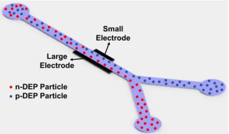
Figure 1.1: Particle separation based on electrical property using AC-DEP
particles in a non-uniform, electric field. These techniques are highly important in particle manipulation and separation [25]. Figure 1.1 shows the schematic of particle separation based on electrical property using AC-DEP.
Broadly, DEP can be categorized into AC-DEP and DC-DEP. In DC-DEP, two end electrodes is considered for applying voltage, and spatial non-uniformity in electric field is created via insulating objects which deforms straight electric field lines [27]. DC electric filed provides the advantages of eliminating need for external pumping and easy fabrication process, while compared with AC-DEP, larger electric potential and medium conductivity are required for manipulation of particles which makes the device vulnerable to the adverse effects of Joule heating and electrothermal flow [28–30]. DC-DEP, AC-DEP and DC-biased AC-DEP have been successfully implemented for the manipulation of micro/nanoparticles within the microfluidic devices [23, 31].
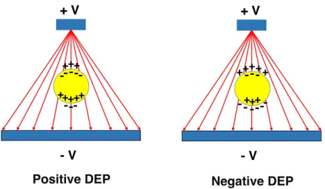
In AC-DEP, asymmetric array of metal electrodes are embedded in a mi-crofluidic device to generate non-uniform electric field. AC DEP separates (bio)particles based on their electrical property and/or size. When the particle has higher polarisability than that of medium, the net force pushes the parti-cle towards small electrode (direction of maximum electric field) which is known as positive DEP (p-DEP). For the case where medium has higher polarisability than that of particle, the net force repels the particles towards the large electrode
+ V - V +
-+ V - V
Positive DEP Negative DEP
+++ +++
-
-
-+ + + ++ +
-++ +
-
-Figure 1.2: DEP force on induced dipoles with the presence of a non-uniform electric field
(direction of minimum electric field strength) which is known as negative DEP (n-DEP). Figure 1.2 illustrates DEP force on induced dipoles with the presence of a non-uniform electric field.
A particle exposed to an electric field, experiences electrostrictive forces aris-ing from accumulation of electrical charges at different interfaces; the charge induction is non-uniform in distribution. Therefore, applied electric field polar-izes the particle into the form of an electrical dipole. For a spherical particle of radius r and applied electric field ~E, the magnitude of induced dipole moment p is given as
p = 4πεmr3fCM(ε, σ, ω) ~E, (1.1)
where fCM known as Clausius-Mossotti Factor (polarisability per unit volume) of
the particle and is determined by conductive and dielectric properties of medium and particle: fCM = ˇ εp− ˇεm ˇ εp+ 2ˇεm , (1.2)
where ˇε is Complex Permittivity which is defined as ˇε = ε − jσ/ω, andfCM Varies
between −0.5 and 1.0.
For a polarized particle in a field gradient, there will be a DEP force acting on a particle, and will result in its motion relative to its medium. In an AC electric field, the time averaged DEP force on a particle is the product of induced dipole
2D Electrodes 3D Electrodes
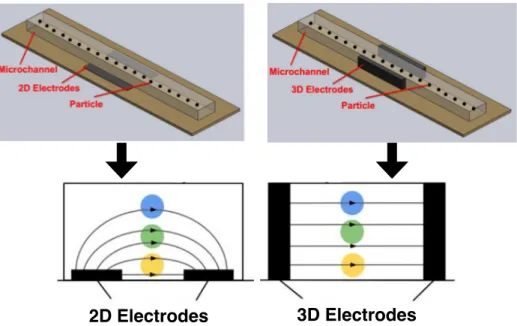
Figure 1.3: Electric field within a microchannel with planar and 3D sidewall electrodes
moment and field gradient which mathematically expressed as: ~
FDEP = (p · ∇) ~E (1.3)
The DEP force acting on the particle is as given ~
FDEP = 2πεmr3fCM(ε, σ, ω)∇| ~E|2 (1.4)
The magnitude of DEP force is affected by particle’s volume, product of local field and local field gradient and electrode geometry. Microelectrodes geometry should produce enough electric field gradient to generate DEP force that over-comes Brownian motion and moves the particle in appropriate direction [23].
In microfluidics application of DEP, a pair of asymmetric electrodes are pro-vided in the system for producing non-uniform electric field within the microchan-nel. Microelectrodes that are fabricated in the bottom layer of microchannel (planar electrodes), produce electrical field along the height of microchannel and result in vertical DEP force on the particles. The electric field is non-uniform and decays exponentially in the height direction of microchannel. Figure 1.3 shows the schematics of device with planar and 3D electrodes and electric field within
a microchannel with planar and 3D electrodes. Due to the decay in the intensity of electric field in vertical direction, the particles that are away from electrodes, experience less DEP force which is not enough for manipulation. Because of this limitation, height of microchannel requires to be less than 50µm which lowers the throughput of devices. This issue can be resolved by providing 3D elec-trode configurations which show unique advantages in microfluidic applications. In addition, 3D electrodes has demonstrated unique advantages in particle ma-nipulation using DEP and number of groups have studied the application and influence of various 3D electrodes topographies in particle manipulation [32–41].
1.2
Objectives and Motivation
The major objective of this thesis is using AC-DEP in microfluidic device for high throughput, continuous separation of particles based on their electrical proper-ties. Non-uniform electric field is generated by employing either pair of 3D, asymmetric, reusable metal electrodes or 3D, asymmetrical, deposited electrodes. The DEP force is produced in the transverse direction to the flow via applying voltage on asymmetric electrodes. The flow is loaded in the microchannel im-plementing laboratory syringe pump. In presented microfluidic systems, DEP force is experienced by particles in specific voltage and frequency while flowing through dielectrophoretic separation region. By employing laboratory syringe pump and providing continuous flow in the microchannel together with localized non-uniform AC electric field, the negative effects originating from high electric field such as Joule heating have been reduced.
1.3
Outline of the Thesis
The complete thesis includes the flowing main parts:
Chapter 1 gives an introduction about microfluidics and Lab-on-a-chip (LOC) technologies. Dielectrophoretic manipulation of particles in microfluidic
devices is described and main characteristics of AC-DEP are mentioned. The equations and expressions of dipole moment, DEP force and motion are pre-sented for a spherical particle. Type of electrode configurations in DEP based microfluidic devices are addressed.
Chapter 2 presents modeling of LOC design for continuous separation of particles based on their electrical property using two different configuration of electrodes, planar and 3D. To make better comparison of design efficiency, bar plots of presenting particle numbers are presented. Feasibility of design is studied by investigating variations in effective parameters in device functionality such as channel size and voltage. The last part of chapter presents the modeling of two new, simple LOC device for continuous separation of particles based on their electrical properties using AC-DEP.
Chapter 3 demonstrates fabrication process of two microfluidic devices for particle separation using AC-DEP. Combination of high precision machining and microfabrication techniques is hired for fabrication of devices. Both devices con-sist in a rectangular microchannel connecting one inlet and two outlets. AC electric fields are produced using either 3D embedded electrodes or 3D deposited electrodes. The fabrication process of each device is presented in detail.
Chapter 4 presents experimental results of fabricated devices. The response of 5µm spherical Latex particles to the flow and electric field are examined. Col-lection of particles in appropriate reservoirs in various flow rates and applied voltages is demonstrated. Experimental results are compared with modeling re-sults and a very good agreement between them are distinguished.
Chapter 5 summarizes and highlights the major findings of the work and ex-plains future research works. This chapter proposes an outlook for integration of proposed DEP device with Acoustophoresis (ACP) device for bio-particles wash-ing, separation and concentration. In addition, implementation of 3D electrodes by employing such configuration for particle counting applications is described.
Chapter 2
Simulation of Particle Motion
This chapter presents modeling of LOC design for continuous separation of par-ticles based on their electrical property using two different configuration of elec-trodes, planar and 3D electrodes. For both cases, the device consists in a rectan-gular microchannel connecting one inlet reservoir and two exit reservoirs. Inlet reservoir is for loading bulk solution through the microchannel and exit reser-voirs are for collection of particles with different electrical properties. In the modeling with planar electrodes, the non-uniform electrical field is produced by implementing two asymmetric, thin layer, 2D electrodes in the bottom layer of microchannel along the x−direction of wall, and in the simulation with 3D elec-trodes, non-uniform electric field is generated by considering 3D electrodes in the channel along the wall. This modeling is implemented to highlight the priority of 3D electrodes over planar electrodes. Moreover, the feasibility of proposed model is studied by investigating variation in the size of microchannel and applied volt-age. In addition to study of feasibility of 3D electrodes under various conditions, the modeling and simulation of a novel device for continues separation of parti-cles is implemented and the results are proposed to make comparison between the results of experimental and numerical techniques. Particle trajectory within the microchannel is modeled using point particle approach and simulation of pre-sented design is implemented utilizing COMSOL Multiphysics software. In order to simulate particle trajectory, some assumptions need to be considered:
liquid has constant thermo-physical properties,
thermal effects on flow field and particle velocity are negligible,
the Reynolds number is much less than one and the flow can be freely considered as creeping flow,
particle rotation does not affect the flow and particle’s translational motion The electric field inside the microchannel could be governed by solving Laplace equation with insulating boundary conditions in the microchannel walls and reser-voirs, and specified electrical potential in the electrodes. As the Reynolds number is low, the flow field inside the microchannel could be described by Stokes equa-tion with no-slip boundary condiequa-tions in the microchannel walls and specified pressure values in the reservoirs.
−∇P + µ∇2~u = 0 (2.1)
The net force experienced by particle is resulted from electric and flow fields. In the limitation of creeping flow, the drag force on particle is described as:
~
Fdrag = 6πµR(~u − ~up) (2.2)
where R is particle radius, ~u is the fluid velocity and ~up is particle velocity [24].
The DEP force acting on particle resultant from electrical field and is described by:
~
FDEP = 2πεmr3fCM(ε, σ, ω)∇| ~E|2 (2.3)
Using second law of Newton, equation of motion for the particle could be described as:
mp
d~up
dt = ~Fext (2.4)
where mp is the mass of particle and ~Fext is the net force on particle.
Regarding above equations, velocity of particle could be governed as:
~ up = ~u − εmr2Re[fCM] 3µ ∇ ~E 2 rms (2.5)
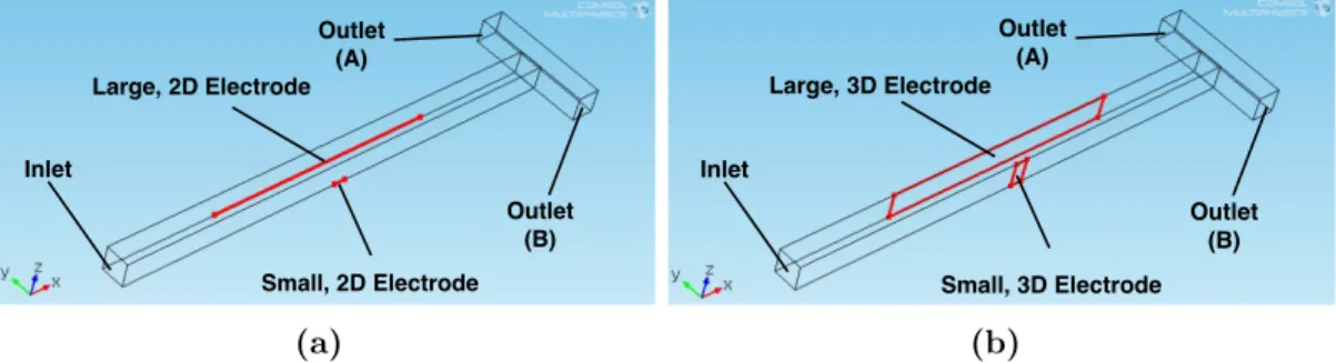
Inlet Outlet (B) Outlet (A) Large, 2D Electrode Small, 2D Electrode (a) Inlet Outlet (B) Outlet (A) Large, 3D Electrode Small, 3D Electrode (b)
Figure 2.1: LOC design with (a) planar and (b) 3D electrode configuration
The particle trajectory of polystyrene, spherical particles are simulated using COMSOL Multiphysics. For simulation, the flow and electric fields need to be computed in the microchannel. Electric field is computed using Electric Cur-rents Physic and solving Maxwell’s equations in specific boundary conditions. In addition, flow filed is calculated by using Laminar Flow Physics and solving Navier-Stokes equation using specific boundary conditions. The particle trajec-tories are simulated by using streamline plot in post-processing and considering particle velocity resulted from Eq. (2.5).
2.1
Comparison of Planar and 3D Electrodes
In the simulations, for the flow field, Navier-Stocks equation is solved considering following boundary conditions: no-slip at the microchannel wall, specific flow rate in the microchannel inlet and zero pressure in the microchannel outlets. For elec-tric field, Maxwell equations are solved with the boundary conditions of insulated in the walls, zero voltage in the small electrode and specific voltage in the large electrode. After obtaining electric and flow field in the microchannels via men-tioned modules, particle trajectories are obtained by using streamline function of COMSOL in postprocessing step. In order to have a random distribution of par-ticles from the inlet, the initial locations of parpar-ticles in the inlet are assigned by using normal distribution function of MATLAB. The schematic drawing of LOC design with planar and 3D electrode configurations are presented in Figure 2.1.
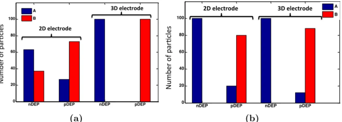
nDEP pDEP nDEP pDEP 0 20 40 60 80 100 Pa rç a c Ûk Sa y Ûs Û A B 2D#electrode# 3D#electrode# Fig#1a# N um be r'o f'p ar ,c le s' (a)
nDEP pDEP nDEP pDEP
0 20 40 60 80 100 Pa rç a c Ûk Sa y Ûs Û A B Fig$1b$ 2D$electrode$ 3D$electrode$ N um be r'o f'p ar ,c le s' (b)
Figure 2.2: Performance of proposed design with planar and 3D electrode config-urations (a) 50 µm × 50 µm, φ = 1 V, (b)100 µm × 100 µm, φ = 4 V, D = 10 µm
As a bulk solution, a mixture of 100 pDEP and 100 nDEP particles is released from inlet reservoir, and number of particles collected in A and B reservoirs are determined. The modeling is implemented for both planar and 3D sidewall electrodes considering 5 µm and 10 µm diameter particles. The value of Re[fCM]
for nDEP and pDEP particles is considered −0.5 and 1.0, respectively. In ideal case, nDEP particles are expected to be collected in outlet A and pDEP particles are supposed to be collected in outlet B. The allocated length for small and large electrodes are 50 µm and 1000 µm along the wall, respectively.
Particle quantification is implemented in post-processing step using MATLAB and bar plots are assigned for each type to clearly show the number of particles in the reservoirs for each of modeling cases. Rectangular microchannels with dimensions of 50 µm × 50 µm and 100 µm × 100 µm are considered and the normal inflow velocity within the microchannel is assigned as 0.005 m/s.
Figure 2.2 shows the performance of proposed design with planar and 3D electrodes. In order to have more comprehensive comparison between the perfor-mance of two electrode types, variation in particle size, channel size and voltage value is considered. A total number of 100 nDEP and 100 pDEP particles are re-leased from the inlet and in ideal case, it is supposed to have 100 nDEP particles in outlet A and 100 pDEP particles in outlet B.
As seen from the Figure 2.2, the implementation of 3D electrodes improves the separation efficiency for the given flow field at the applied voltage. Figure 2.2–(a)
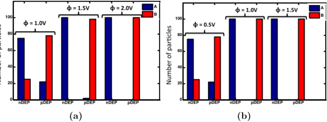
nDEP pDEP nDEP pDEP nDEP pDEP 0 20 40 60 80 100 Pa rç a c Ûk Sa y Ûs Û A B ϕ!=!1.0V! ϕ!=!1.5V! ϕ!=!2.0V! Fig!2a! N um be r'o f'p ar ,c le s' (a)
nDEP pDEP nDEP pDEP nDEP pDEP
0 20 40 60 80 100 Pa rç a c Ûk Sa y Ûs Û A B Fig$2b$ ϕ$=$0.5V$ ϕ$=$1.0V$ ϕ$=$1.5V$ N um be r'o f'p ar ,c le s' (b)
Figure 2.3: Voltage variation effect on separation efficiency of proposed design (a) 50 µm × 50 µm, (b)100 µm × 100 µm, D = 10 µm
clearly states that the microchannel of 50 µm × 50 µm size, with 3D electrodes is able to reach desired output, but the same microchannel with planar electrodes cannot catch the ideal case. For microchannel with size of 100 µm × 100 µm, to have similar output with planar electrodes, voltage needs to be increased and with 3D electrodes, pDEP particles are not separated completely and some of them can be found in reservoir A. Therefore, for larger microchannel in size, use of 3D electrodes still cannot reach the ideal output, while it is clear that separation efficiency improves in comparison with similar case with planar electrodes.
Figure 2.3 shows the effect of voltage variation on separation performance of presented design with 3D sidewall electrodes. Simulation results confirms that separation efficiency increases by increasing the value of applied voltage, which is expected, since increasing voltage leads to enhanced DEP force on particles. However, increasing voltage introduces Joule heating within the microchannel. Joule heating is not a desirable phenomenon, since it may cause negative effects like bubble generation and bioparticles damage, which lowers device functionality and performance [35].
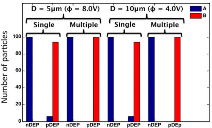
One possible way to increase separation efficiency instead of increasing volt-age, is implementation of multi-teeth small electrodes. Figure 2.4 compares par-ticle separation with using single-top and multi-tip small electrode for 10 µm and 5 µm particles. Implementing multi-tip small electrode for separation provides the possibility of applying DEP force on particle in several stages, and causes
nDEP pDEP nDEP pDEP nDEP pDEP nDEP pDEp 0 20 40 60 80 100 Pa rç a c Ûk Sa y Ûs Û A B
Single! Multiple! Single! Multiple! D = 5μm (ϕ = 8.0V) D = 10μm (ϕ = 4.0V) N um be r'o f'p ar ,c le s'
Figure 2.4: Effect of number of tips on small electrode
repulsion/attraction of particles to be more sufficient.
2.2
Device Modeling
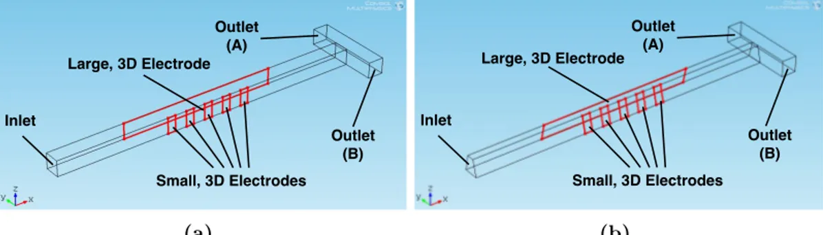
This part presents the modeling of two novel, simple LOC device for continuous separation of particles based on their electrical properties using AC-DEP. One device is fabricated by implementing high precision machining technique for man-ufacturing of external and reusable electrodes, and the other device is fabricated by utilizing metal coating on the microchannel wall via sputtering. The schematic designs of both devices are presented in Figure 2.5.
The device with reusable electrodes, consists of a rectangular microchannel connecting one inlet and two outlets and the non-uniform electric field is generated via one large electrode and a five-tip small electrode. The chip with sputtered electrodes is composed of a trapezoidal microchannel connecting one inlet and two outlets and pair of asymmetric electrodes (one large and a five-tip small) for generating non-uniform electric field.
The particle trajectories of polystyrene particles (5 µm in diameter) are sim-ulated in COMSOL Multiphysics. In both devices, the large electrode has length of 6 mm and small electrode consists in five 400 µm tips along the wall. For the flow field, Navier-Stocks equation is solved considering boundary conditions of
Inlet Outlet (B) Outlet (A) Large, 3D Electrode Small, 3D Electrodes (a) Inlet Outlet (B) Outlet (A) Large, 3D Electrode Small, 3D Electrodes (b)
Figure 2.5: Schematic of LOC device (a) with reusable, 3D electrodes and (b) with deposited, 3D electrodes
no-slip at the microchannel wall, specific flow rate in the microchannel inlet and zero pressure in the microchannel outlets. For electric field, Maxwell equations are solved with the boundary conditions of insulated in the walls, zero voltage in the small electrode and 10 Vpp in the large electrode. In simulations the value of
applied voltage need be entered as rms values, so considered voltage for this set of simulation is entered as 5 Vrms for suare signals. A mixture of 500 pDEP and
500 nDEP particles is released from the inlet reservoir, and number of particles collected in outlets A and B are determined.
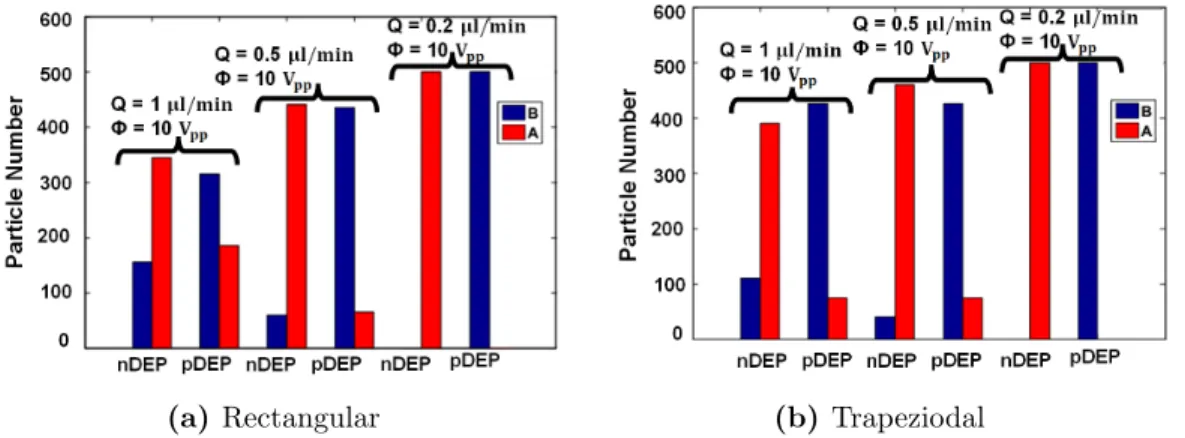
In order to analyze the feasibility of devices, both are examined for three differ-ent values volumetric flow rates and results are presdiffer-ented in suitable bar plots to compare devices efficiency for high, medium and low flow rates in the microchan-nel. For both devices, the values of 1 µl/min, 0.5 µl/min and 0.2 µl/min for flow rates are considered as high, medium and low flow rates, respectively. Figure 2.6 shows the devices performance in three different flow rates with constant value of 10 Vpp as applied voltage.
Modeling results present that for fixed value of voltage, flow rate plays an important role in determining device performance. In high flow rates, particle will leave separation region very fast and would not let DEP to make them separated, but low flow rates provides enough time for DEP force to attract or repel particles and separate them according to their electrical properties. For both devices, reducing flow rate from high to low provides good results for particle separation for constant voltage of 10 Vpp.
(a) Rectangular (b) Trapeziodal
Figure 2.6: Performance of the devices with different flow rates (φ = 10 Vpp): (a)
rectangular-microchannel, (b) trapezoidal-microchannel
(a) Rectangular (b) Trapeziodal
Figure 2.7: Performance of the devices with different voltages and flow rates: (a) rectangular-microchannel, (b) trapezoidal-microchannel
In order to study the feasibility of devices in higher flow rates and to in-vestigate device performance for obtaining high throughput separations, another set of simulation has been investigated. Flow rates of of 2 µl/min, 4 µl/min and 6 µl/min are considered. In each flow rate, the voltage is increased step by step until obtaining complete particle separation. Figure 2.7 shows performance of devices with rectangular and trapizoidal microchannels, respectively, in higher flow rates and specific voltage in each case.
Similarly, a mixture of 500 pDEP and 500 nDEP particles is released from inlet reservoir, and number of particles collected in outlets A and B are determined. In high flow rates, particles leave separation region very fast and larger DEP force
is required to separate particles. Increasing the value of applied voltage results in increasing generated DEP force by non-uniform electric field to quickly repel or attract particles towards desired electrode.
Chapter 3
Fabrication of Devices
In addition to scaling down of laboratory functions to a tiny chip, microfluidic devices provide wide variety of advantages, such as lowering production costs, in-creasing functionality and efficiency. Microfluidic devices can be fabricated from many types of materials with various fabrication techniques proposed in the lit-erature. Basically, there are two approaches for the fabrication of microfluidic devices, substrate based (photolithography) and mold based (soft lithography). Mold-based techniques are very suitable for mass production since once the mold is fabricated, the mold could be used for several times. Therefore, this technique provides a convenient and low-cost platform for fabrication of microstructures. One common material used in the fabrication of the microchannels is the Poly-dimethylsiloxane (PDMS) due to its low cost, low toxicity, ease of fabrication and transparency. One important alternative to fabricate microfluidic devices is us-ing high-precision mechanical machinus-ing for direct substrate manufacturus-ing and mold fabrication.
One alternative to fabricate the microfluidic device is to use mechanical mi-cromachining (i.e. micro-milling) either for direct substrate manufacturing or for the fabrication of the mold. For the direct substrate manufacturing, the limits of the process is constrained by the size of the milling tool which may lead to unsatisfactory end-product for microfluidic applications. However, for the fabri-cation of the mold, the limits of the process is constrained with the xyz-accuracy
and resolution of the tool positioning system of a CNC (Computer Numerical Control)-machine, since the negative of the microfluidic structure is fabricated as a mold. With today’s technology, by using magnetic bearings for their position-ing systems, the xyz−accuracy of precision in CNC-machines are in nanometer ranges. Therefore, a mold can be fabricated using mechanical machining in the order of hours without any need for clean-room equipment within the desirable accuracy limits for microfluidic devices. Moreover, CNC-machining can generate 3D structures without any difficulty [42] (this is also doable with lithography-based methods with some additional steps, not straightforward though).
Common mold materials for mold-based techniques are silicon (quartz/glass), SU-8 photo-resist, polymer based materials (e.g. Plexiglas) or any metal based materials (titanium, stainless steel, and brass). Polymer- and metal-based mold materials are superior over silicon or photo-resist based mold materials in terms of the durability and robustness. In the case of mechanical micro-machining, any of these materials can be selected. However, machinability, cost and the expected life-span of the mold are the important parameters which need to be considered during the selection of the mold material. Another important parameter is the expected life of the mold. However, using metal-based materials comes with a price. Metal based materials’ machining is costly due to the reduced tool life and the increased machining time. On the other hand, machining of polymer based materials is less problematic in terms of tool life and machining time, yet the mold still can be used for many times.
There are two common configuration for asymmetric pair of microelectrodes to generate electric field gradient that is required for the DEP manipulation: planar (2D) and 3D electrodes. Most of the traditional DEP devices are made of planar microelectrodes which are normally thin film metal layer (thickness< 1 − 2 µm) patterned on the bottom floor of microchannel. Fabrication process of 2D elec-trodes always consists of photolithography, thin film deposition and lift–off. Pho-tolithography technique transfers microelectrode pattern from mask to photore-sist. In thin film deposition step, thin layer of metal is deposited on substrate using thermal evaporation or sputtering techniques. After metal deposition, sac-rificial photoresist layer is removed by submerging the substrate in appropriate
solvent. In addition, a thin metal layer could be patterned directly in the ab-sence of photolithography and etching by using laser ablation or deposition via a shadow mask [22, 43]. Such planar electrodes generate fringe like electric field and make the DEP force effective in the vicinity of the electrodes [31]. One alter-native to this issue is to use 3D electrode structures at the sidewalls. With such a configuration, uniform DEP force field in the height direction can be generated. Such a device may generate an effective DEP force in the lateral direction to the flow throughout the height of the device which is very suitable for continu-ous flow separation devices. Varicontinu-ous and more complicated techniques have been developed for fabrication of 3D electrode structures which generate electric field gradient in larger volume of the microchannel. Regarding the application of DEP device, 3D electrodes could be categorized as top–bottom patterned, extruded from microchannel bottom and sidewall configurations [22].
In DEP applications, facing 3D sidewall electrodes has a unique advantage since the resulting electric fields is homogenous in the height direction of mi-crochannels, therefore the area where the DEP force in effective is not confined at the bottom of the microchannel as in the case of planar electrodes. Despite all of these advantages, fabrication of vertical electrodes requires considerable challenge and effort. Regarding this importance, different 3D electrodes for DEP applica-tions have been developed and presented [22]. Iliescu et al. [44] proposed using highly doped silicon as an electrode and fabricating 3D electrodes, and managed to separate viable and non-viable yeast cells [45]. Wang et al. [46] proposed the fabrication of 3D electrodes at the sidewalls by electroplating, and utilized this structure for flow cytometry [47] and continuous separation of human-kidney cells and N115 mouse-neuroblastoma cells by AC-DEP [48]. Kang et al. [49], and Cetin et al. [50, 51] fabricated 3D copper electrodes with an extended-photolithography technique and embedded them along the sidewalls to implement the continuous separation of polystyrene particles and cells by size [49,50] and by electrical prop-erties [51]. Demierre et al. [52] proposed using side channels (what they called ’access channels’) filled with buffer solution and in touch with the electrodes to shape the electric field in 3D without any need for an additional 3D electrode fabrication step. They utilized focusing microparticles [52], and sorting viable
and non-viable yeast cells [53, 54] by this design. In order to provide number of potential advantages including high thermal durability and fracture toughness for microfluidics applications, metallic materials are utilized in the fabrication of microfluidic devices. Recently, titanium micromachining and multilayer lami-nation method has been implemented for fabrication of dielectrophoresis device with planar and sidewall electrodes. Floor electrode device is utilized for size based separation of polystyrene spheres. Moreover, sidewall electrode device is used for Z–dimension flow visualization of polystyrene particles for nDEP and pDEP analyzing [36]. In this fabrication process, pre-fabricated titanium foils are utilized which provide limitation of repeatability of fabrication technique and performance of fabricated device. Foils thicker than 25 µm can be processed be-cause of preventing possible bending and damage during the bonding process. Since titanium foils bonded inside the microchannel wall, thicker foils may be kind of barrier in the microchannel and deviate the laminar flow direction and symmetry. Duarte et al. [55] and Jaramillo et al. [56] proposed the use of 3D car-bon electrodes which are fabricated by C-MEMS technique for superior filtering efficiency. Use of carbon electrodes also minimized the possibility of electrolysis since carbon is chemically more stable than metals. They successfully trapped yeast cells from the mixture with polystyrene particles [55], and E.coli bacteria from a mixture with B.cereus bacteria [56]. Lewpiriyawong et al. [57] proposed the use of conductive PDMS (the PDMS was mixed with gold-powder to make it conductive) as 3D sidewall electrodes, and utilized AC-DEP for the continuous separation of 10 µm and 15 µm polystyrene particles. A new fabrication process has been reported to realize pillar electrode array with metal coverage on the vertical sidewalls. Fabrication process of creating 3D electrodes consisted of two vital steps: metallization of vertical sidewalls of pillar and patterning the metal from the space between pillars [37]. The adjusted distance between pillars was in order of micron and patterning metal from this distance is of high challenge. There is high possibility to damage the metalized pillar while patterning the metal layer between them. Due to high challenge of fabrication in the two vital steps, fabricated device will not be reproducible and have required robustness. A sandwich structure of glass/silicon/glass with 3D electrodes is proposed for di-electrophoretic application of microfluidics. The silicon layer defines the walls and
electrodes of DEP device. The 3D sidewall electrodes generate uniform DEP force in the microchannel and producing velocity gradient in the device [38]. The main steps in fabrication of device were wet and dry etching of thick glass and silicon substrates. Total fabrication process requires four etching step which consumes considerable time and results in fabricating a device with weak capability of mass production. In order to improve the performance of cell and particle trapping by DEP, 3D metal pillars have been developed via electroplating. Fabrication of the device, employs two steps of deposition and patterning of SU-8 and electroplat-ing cylindrical gold electrodes [39]. Separate from fabrication of whole device, these steps require considerable time to be passed in the cleanroom because for each step of SU-8 patterning, a new mold should be fabricated. In addition to this limitation, another issue which should be considered is that gold is an ex-pensive material and cannot be used broadly in disposable chips. Considering mentioned points, biological applications demand for microfluidic devices which are cost-effective and time-effective. A DEP device with vertical electrodes has been fabricated for multiplexed switching of objects [40]. Fabrication techniques of SU-8 photolithography, metal deposition and electroplating were used to make the microchannel and electrodes, respectively. Experimental results for switching cells and polystyrene beads to multiple outlets have been presented. As previously discussed, fabrication of this device needs multi-step process which take consid-erable time and require expensive facilities in a clean-room. A novel technique is demonstrated to construct arc-shaped, 3D electrodes at the microchannel wall by utilizing low melting point bismuth (Bi) alloy (melting point is around 47◦C) [34]. To show the application of presented microfluidic device, manipulation of parti-cles and cell–particle and particle–particle separation were conducted using DEP. Bi microspheres were produced using a specific device and were positioned at the sidewall. In order to have easy and accurate placement, microspheres should not be very tiny. In the other hand, in order to have laminar and symmetric flow rate, microspheres should not be large compared to the channel size. The bonding pro-cess would not provide a robust microfluidic device and in the condition of high flow rates, the possibility of damaging the electrodes is very high. An AC-DEP continuous bio-particle sorter using 3D travelling-wave was presented for sepa-ration of red blood cells from debris-filled heterogeneous, as well as size-based
separation of poly-dispersed liposome suspensions [58]. Employed techniques for main steps of fabrication of the device are deposition by electro-beam evapora-tor, photolithography, etching, lithography, diamond drilling and adhesion by UV curable glue, respectively. Device fabrication is of poor controllability because of need for high precision and sensitivity that should be considered at each step. For continuous separation of particles and cells, 3D electrodes was used to generate non-uniform electric field in the height of microchannel. Microchannel was fabri-cated following soft lithography procedure and copper electrodes were prepared to be inserted into the PDMS electrode chambers manually under the micro-scope [51]. In the fabrication process, there are some critical steps which highly affect fabrication repeatability: obtaining thin copper microelectrodes without any damage and bending and inserting electrodes appropriately for generation of non-uniform electric field. Since, the electrodes are inserted manually, there are high possibilities for damaging and misplacement during the insertion of the elec-trodes. Metal inkjet printing technique is employed for fabrication of 3D micro electrodes for bio-applications of DEP and nDEP characteristics of polystyrene particles are observed because of trapping on Ag electrodes. Fabrication process of DEP device concisely consists of lift-off, standard photolithography, Fluorocar-bon coating and inkjet printing. Fabrication process is not very straightforward and implementing multi photolithography technique is required. Moreover, one of the vital and difficult to control steps is protecting alignment of Au elec-trodes with coated Fluorocarbon. Because any misalignment in this case may result in over spreading in inkjet printing step and fabrication of the device with damaged electrodes [59]. Ion-implantation technique is utilized for patterning of 3D electrodes in a microfluidic device of DEP platforms. The proposed de-vice was implemented for electro–orientation within the microchannel to align the bacteria to the electric field and to move the particles to the middle of mi-crochannel with functionality of combination of large mimi-crochannels with smaller structures. Similarly, microfabrication techniques as photolithography, sputter-ing, soft lithography and ion-implantation are employed to produce final device. In order to create electrodes on the walls of microchannel, the ions are implanted at a specific angle. Similar to previously mentioned fabrication techniques, pro-viding the correct angle and keeping it constant by the end of process is of high
challenge [60]. More information about the fabrication techniques of DEP devices for particle manipulation and separation could be found elsewhere [22, 61].
Moreover, all of discussed techniques for the fabrication of microfluidic devices with 3D sidewall electrodes require lithography or MEMS-based fabrication tech-niques which usually requires multi-step process which take considerable time, and require expensive and high technology facilities in a clean-room environ-ment [47, 62]. These fabrication techniques also have a geometric limitation on the channel height which is important when the throughput of the device is con-cerned. In this thesis, two alternative fabrication techniques has been proposed for the fabrication of a microfluidic device with 3D sidewall electrodes namely (i) mechanical machining based method (MMM) and (ii) hybrid method (HM). Both techniques utilize the high precision mechanical machining of the mold structure. MMM also utilizes mechanical machining of the electrode structure. On the other hand, HM uses electrode deposition by using a shadow mask which is also fab-ricated by WEDM. The details of these techniques are given in the upcoming sections.
3.1
Mechanical Machining based Method (MMM)
The device with embedded, reusable electrodes is a PDMS microfluidic chip con-sisting a rectangular microchannel which connects one inlet and two outlets, and has been bonded to a glass substrate (25 × 75 × 1 mm3) following mold based
fab-rication technique. The master mold for casting PDMS is fabricated from brass using high precision mechanical machining. High precision machining of stainless steel is hired for fabrication of reusable micro electrodes. Detailed fabrication process of device is described below.
3.1.1
Fabrication of the mold
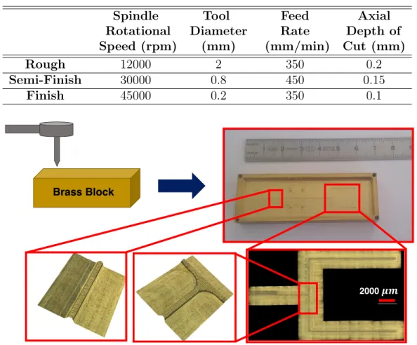
Fabrication of mold with micro-features is of significant importance which di-rectly dictates the quality of the microchannels in the microfluidic device. The fabrication process of these molds demand for special attentions in preparing CAM (computer aided manufacturing) program and machining process. In the development of CAM program adaptive feed rate control options together with interpass cleaning strategies are used. Micromilling operations is conducted on a DECKEL MAHO-HSC55 milling center equipped with HES510-HSKA63 high speed spindle with a run out less than one 1 micron. In order to have a better con-trol on Z-levels the mold is mounted on a KISTLER-9256C1 mini-dynamometer. Very fine grain Tungsten Carbide micro-end mills (NS Tools-MSE230) are used for micromilling operations.
Machining steps of the fabrication process is as follows:
(1) Face milling operation with a 2 mm diameter end mill to ensure flatness of stock surface
(2) Pocket milling to open mold cavity
(3) Contour milling of the microchannel and the guide pins
(4) Drilling operation for M2 screws in the sides of the mold
(5) Tap milling for M2 screws in the side of the mold
The machining parameters of the mold are tabulated in Table 3.1. Microchan-nel has the height of 100 µm, width of 100 µm and length of 55 mm. In order to have robust pipe connection in the reservoirs, the depth of the microchannel cavity has chosen as 3 mm.
Figure 3.1 shows the fabricated brass mold. Microscopic images of different regions of mold are also provided to show the high precision machining perfor-mance. Screws in the two sides of the mold are considered to apply force and
Table 3.1: Machining parameters of brass mold
Spindle Tool Feed Axial Rotational Diameter Rate Depth of Speed (rpm) (mm) (mm/min) Cut (mm)
Rough 12000 2 350 0.2
Semi-Finish 30000 0.8 450 0.15
Finish 45000 0.2 350 0.1
2000 𝝁𝒎
Brass Block
Figure 3.1: Fabricated brass mold and microscopic images
prevent the leakage of the PDMS between the tips of the electrode and microchan-nel. For each electrode two guide pins are considered within the mold for easy placement of electrodes.
3.1.2
Fabrication of the electrodes
Fabrication of electrodes consists in two separate steps: micromilling and Wire Electric Discharge Machining (WEDM). Micromilling operations is conducted on a DECKEL MAHO-HSC55 milling center equipped with HES510-HSKA63 high speed spindle. The machining parameters are shown in Table 3.2. The
profile of the tips in small electrode and external contours are cut by Sodik-AP250L WEDM machine. A Zinc coated Brass wire of 0.1 mm in diameter is used for WEDM process. The machine uses EDMFluid-108MP/S as a dielectric fluid which highly reduces the EDM gap and over-cut and results in parts with high accuracy and surface quality. Mainly, seventeen different parameters can be adjusted to obtain an optimum cut. For the fabrication of electrodes one rough cutting and six finish cutting are performed.
1 mm-in-depth stainless steel sheet has been utilized for manufacturing pair of asymmetric electrodes. Large electrode is 9mm in length and 5 mm in width. The small electrode has five tips in length of 400 µm and the same width as large electrode. The space between tips in small electrode is 1 mm. Two elliptic guide slots are considered to have easy placement of electrodes in the mold and ensure robust contact with microchannel wall. Bottom sides of the electrodes have cavities for the ease of removal process of the electrodes from the mold during the peel-off, and for a better sealing at bottom side of the electrodes when the PDMS layer is bonded to the glass.
Machining steps of the fabrication of electrodes could be summerized as below:
(1) face milling operation to ensure smoothness of stock surface
(2) pocket milling for cavity and guide slots
(3) contour milling for outside of the stock
(4) WEDM contour cutting of tips
Table 3.2: Machining parameters electrodes
Spindle Tool Feed Axial Rotational Diameter Rate Depth of Speed (rpm) (mm) (mm/min) Cut (mm)
Rough 25000 0.8 400 0.15
2000 𝝁𝒎 2000 𝝁𝒎 2000 𝝁𝒎 2000 𝝁𝒎 500 𝝁𝒎 Stainless Steel Sheet
Figure 3.2: Fabricated small and large electrodes
The fabricated electrodes are presented in Figure 3.2. Three dimensional microscopic images confirms the good surface quality of electrodes in the regions which would be in contact with microchannel wall.
3.1.3
Assembly of the microfluidic device
After the fabrication of the mold and electrodes, the microfluidic device was ready to be assembled. The assembly process of the microfluidic device can be summarized as follows:
(1) Electrodes were placed at the desired location of the mold by aid of guide pins.
(2) The screws at the side wall were tightened to apply pressure at the interface between the electrodes and the microchannel to prevent the leakage of the PDMS to the interface
Figure 3.3: Assembly of electrodes and mold
the mold. At this step, special care was taken to prevent any air trap in the grooves of the electrodes.
(4) The device was placed in an oven to cure the PDMS (75◦ C for 90 min). (5) Screws and upper plate were removed from the system. Once the screws
at the top were removed, two openings which would be used for electrical connections to the electrodes remained.
(6) PDMS was peeled off from the mold. Electrodes were also peeled of very easily with the help of the grooves filled with PDMS.
(7) The reservoirs were punched out.
(8) A clean glass slide and the PDMS were plasma treated, and bonded to get the final device.
Assembly of electrodes and mold is presented in Figure 3.3, fabrication steps are summarized in Figure 3.4. After completion of microdevice fabrication, the
PDMS Casting
Peeling PDMS Plasma Bonding
to Glass
Figure 3.4: Fabrication process of microfluidic device with reusable, 3D electrodes using MMM
final device was checked under the microscope to see any fabrication defects. Finally, water was loaded to the system to check the bonding and any possible leakage. The water and ink mixture was also tested. The system was free of defects, and no leakage was observed. The microfluidic device with reusable, embedded, 3D electrodes is shown in Figure 3.5
3.2
Hybrid Method (HM)
The device with deposited, 3D electrodes is a PDMS microfluidic chip consisting a trapezoidal microchannel which connects one inlet and two outlets and has been bonded to a glass substrate (25×75×1mm3). The master mold for casting PDMS is fabricated from stainless steel using high precision micromachining. Specific electrode pattern has been generated by implementing sputtering and metallic shadow mask which has required durability to be used in the box coater. High precision machining of stainless steel sheet is hired for fabrication of shadow mask. Detailed fabrication process of device is proposed below.
3.2.1
Fabrication of the mold
Fabrication of master mold starts with CAD designing of the device. Trapezoidal microchannel profile has been preferred for this mold due to generating deposited metal layer in the microchannel wall which provides 3D electrode configuration for the device. Machining parameters for fabrication of this mold is the same as previously described brass mold.
Machining steps of the fabrication are as following:
(1) Face milling operation to ensure smoothness of stock surface
(2) Pocket milling to open mold cavity
Figure 3.6: Fabricated stainless steel mold and microscopic images
Microchannel has the height of 100 µm, width of 100 µm and length of 55 mm. In order to have robust pipe connection in the reservoirs, the depth of the mi-crochannel cavity has chosen as 3 mm. Figure 3.6 shows the fabricated stainless steel mold. Microscopic images of different regions of mold are also provided to show the high precision machining performance.
3.2.2
Fabrication of the shadow mask
Same WEDM machine used for the fabrication of electrodes is used for shadow mask fabrication. Since we have a very thin feature at the middle of the shadow mask it is very susceptible to be burnt off therefore, an optimum set of WEDM parameters are essential.
Thin sheet of stainless steel (0.8 mm-in-thickness) and consists in two grooves resembling small and large electrodes configurations. The groove which repre-sents large electrode is in shape of rectangle with 6 mm in length and 7 mm in width. The other groove consists in five tips with length of 400 µm and represents small electrode and has the same width with the groove of large electrode. The
500 𝝁𝒎 500 𝝁𝒎 100 𝝁𝒎
Stainless Steel Sheet
Figure 3.7: Fabricated shadow mask and microscopic images
minimum distance between the grooves is 40 µm. Figure 3.7 illustrates fabricated shadow mask by using WEDM.
3.2.3
Assembly and fabrication of microfluidic device
After completion of the master mold and shadow mask fabrication, microfluidic device is ready to be fabricated. The summary of fabrication process of the microfluidic device is presented here.
(1) PDMS and curing agent were mixed in the ratio of 10:1, and poured into the mold. At this step, special care was taken to prevent any air trap in the polymer, especially regions around the microchannel.
(2) The device was placed in an oven to cure the PDMS (75◦ C for 90 min). (3) PDMS was peeled off from the mold.
(4) A clean glass slide and the the back side of PDMS plate were plasma treated, and bonded.
PDMS Casting Peeling off PDMS Plasma Bonding to Glass Aligning Shadow Mask and Sputtering Plasma Bonding to PDMS Layer
Figure 3.8: Fabrication process of the microfluidic device with 3D, deposited electrodes using HM
(5) Shadow mask was gently and accurately aligned on the PDMS plate, such that the thin barrier between two grooves of mask locates exactly in the middle of microchannel.
(6) The assembled setup was taken to box coater and 500 nm Cr was deposited on the device using sputtering technique.
(7) The shadow mask was separated from the PDMS plate.
(8) A PDMS layer with punched out reservoires was prepared and was bonded to the glass/PDMS sandwich using plasma treatment for fabrication of final microfluidic device.
Fabrication process of the microfluidic device with 3D, deposited electrodes and photograph of final device are presented in Figure 3.8 and 3.9, respectively.
Figure 3.9: Microfluidic device with deposited, 3D electrodes using HM
3.3
Assessment of the Fabrication Techniques
This chapter presented fabrication process of two different, new and simple mi-crofluidic devices for continuous separation of particles and cells based on their electrical property by using AC-DEP. For both devices, molds were fabricated using high precision machining. For one device, metal electrodes have been fabri-cated using high precision machining, and were embedded into the device during the molding process. For the other device, after molding process, thin layer of metal has been deposited on microchannel wall employing sputtering technique. Two fabrication processes were described for two microfluidic devices in detail. The advantages offered by the proposed fabrication techniques could be listed as:
(1) Fabricated molds could be used for many times without any damage. (2) Fabrication of a mold with tilted sidewalls and/or with varying channel height
(3) Fabricated electrodes are reusable and could be safely removed from the chip before disposing.
(4) Device assembly is straightforward and does not require any specific device or tool.
(5) Fabrication of chips could be performed in normal laboratories and clean-room environment and facilities are not required.
(6) Unique design of reusable electrodes provide robust bonding between PDMS layer and glass substrate, and prevents any leakage of fluid while pumping through the microchannel.
(7) Fabricated shadow mask is robust and durable, and could be used many times.
(8) Fabrication of device with deposited electrode provides possibility of fabri-cating finer electrode structures.
(9) Fabrication processes are highly repeatable and reproducible.
(10) Fabrication processes are time and cost-effective with microchannel struc-tures without sharp edges.
In fabrication of devices, there are some points which should be considered to keep the key elements away from damage and fabricate the devices with good functionality. In inserting the reusable electrodes, the tightening of screws in the sides of the mold should be performed gently to maintain the channel wall from tip print of small electrodes. In fabrication of the chip with deposited electrodes, the shadow mask should be aligned on the PDMS layer such that the thin feature be in the center of microchannel guarantee the deposition of metal layer on the microchannel sidewall. One of the vital parameters which should be considered in designing trapezoidal microchannel is the value of acute angle. In order to obtain 3D sidewall electrodes, the angle should be considered such that provide full covering of channel bottom by thin feature of shadow mask and full exposure of channel sidewall by metal atoms in the box coater. Because of the specific
values of the height and width of microchannel in proposed device, the acute angle in trapezoidal microchannel has been chosen as 76◦.
In fabrication with mechanical machining method, height of microchannel should not be less than 100 µm due to the ease of placement of the electrodes and the device assembly. Although it has not been demonstrated, MMM is less problematic for the channels with the height higher than 100 µm, and the height of the channel can easily reach up to 500 µm. For HM, the fabrication may be problematic as the height goes below 50 µm and as the height goes above 150 µm due to the difficulty in placing the shadow mask, and it will be difficult to obtain the desired geometry. Therefore, depending on the desired channel height of a microfluidic device, the appropriate fabrication technique may be chosen.
Chapter 4
Experimentation and Results
Following the fabrication of both devices, the final microfluidic devices are uti-lized for experimentation. The aim of the experimentation is to demonstrate the manipulation of 5µm latex particles with nDEP force (i.e. pushing towards large electrode and collecting in Reservoir A located at the same side with the large electrode). 5 µm diameter latex particles (LATEX SPHERES BCR–Certified reference material) with a mass concentration of 2 g/ml is used to examine the device feasibility and performance for the manipulation of nDEP particles. Spe-cific value of particle solution is washed by DI water to prevent contamination and the sticking of the particles on the channel walls. has been diluted with the specific amount of DI water to obtain the desired particle concentration in the buffer solution. Following the washing, the particles are suspended in a spe-cific amount of buffer solution with conductivity of 360 µS/cm which is measured by using conductivity meter (HANNA Instruments, HI 9812-5). Properties of medium (buffer solution) and particles are summarized in Table 4.1. Laboratory syringe pump (New Era Pump Systems-NE 300) is used to load the bulk solu-tion from inlet reservoir through the microchannel, and flexible and transparent tubes with inner diameter of 3 mm has been implemented as the interface of the syringe pump and the inlet hole. A function generator (AGILENT 33250A) has been used to generate square waves with specific voltage and frequency. In order to produce required voltages in higher frequencies, an amplifier (Falco Systems
Figure 4.1: Experiment setup of microfluidic devices
WMA-300) has been located in the electrical manipulation circuit. The particle motion is monitored by an inverted optical microscope (K3DI 3D Microscope Converter System by AIV Labs). Figure 4.1 shows the photo of the experiment setup.
The feasibility and the manipulation performance of each device are examined and the results are compared with the simulation results. The particle motion is recorded and particle trajectories within each device are generated with post-processing of the images. The experimental conditions and results of each device is presented and discussed in detail in the following sections.
Table 4.1: Properties of the particles and medium Medium Particle Density (gr/cm3) 1 1.05
Permitivity 80 2.5 Conductivity (µS/cm) 360 1