Dark current reduction in ultraviolet metal-semiconductor-metal
photodetectors based on wide band-gap semiconductors
Serkan Bütün1, Mutlu Gökkavas2, HongBo Yu2, Vlodek Strupinski3 and Ekmel Özbay4
1
Nanoteknoloji Araştıma Merkezi and Fizik Bölümü, Bilkent Üniversitesi, Ankara, Türkiye
2
Nanoteknoloji Araştıma Merkezi, Bilkent Üniversitesi, Ankara, Türkiye
3
Institute of Electronic Materials Technology, 01-919 Warsaw, Wolczynska 133 Str., Poland
+
Nanoteknoloji Araştıma Merkezi and Fizik Bölümü and Elektrik ve Elektronik Mühendisliği Bölümü, Bilkent Üniversitesi, Ankara, Türkiye
Abstract
Photodetectors on semi-insulating GaN templates were demonstrated. They exhibit lower dark current compared to photodetectors fabricated on regular GaN templates. Similar behavior observed in photodetectors fabricated on epitaxially thick SiC templates.
Summary
Here we present our work on metal-semiconductor-metal (MSM) photodetectors on semi-insulating GaN templates (Figure 1a). Epitaxial growth of the samples was performed in a metal organic chemical vapor deposition reactor. We also fabricate MSM photodetectors on regular unintentionally doped GaN template (Figure 1b) for an evenhanded comparison. Devices on semi-insulating template exhibited four orders of magnitude lower compared with devices on regular template (Figure 2). A dark current density of 1.96×10⁻¹⁰A/cm2at 50 V bias was measured for photodetectors on semi-insulating template. Spectral responsivity measurements were carried out. Photodetectors fabricated on the semi-insulating template was able to detect incident optical power of as low as 3 pW at 360 nm illumination.
236
TuM4 11.15 - 11.30
Figure 1: Epitaxial structures of (a) semi-insulating (b) unintentionally doped GaN templates.
Figure 2: Current-Voltage characteristics comparison of the MSM photodetectors.
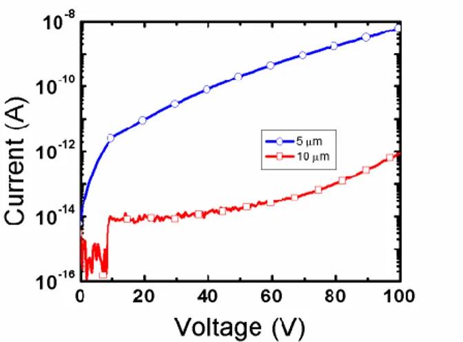
We also show our efforts on SiC based metal-semiconductor-metal photodetectors epitaxially grown on SiC templates. The epitaxial growth was performed by using a chemical vapor deposition system. The effect of the growth thickness on device performance was investigated by undoped SiC layers of different thicknesses (5 micron and 10 micron), which were grown on 4H-SiC substrate. The photoluminescence intensity of the 10 micron thick template was twice as high (Figure 3). The devices grown on the 10 micron thick template showed a dark current density 4.4 × 10⁻¹¹A/cm2under 50 V reverse bias voltage, which was four orders of magnitude lower than those devices grown on the 5-micron template (Figure 4). The peak responsivity for the 10 5-micron thick sample was 7.2 × 10⁻²A/W, under 303 nm UV illumination and 25 V reverse bias. The corresponding peak responsivity for the 5 micron thick sample was 7.3 × 10⁻²A/W, at 273 nm UV illumination and 25 V reserve bias.
Figure 3: Normalized PL spectrum of the SiC epitaxial layers. Data is normalized to maximum of the red curve.
Figure 4: IV Characteristics of the SiC MSM photodetectors.