Topical Review
Atomic layer deposition: an enabling
technology for the growth of functional
nanoscale semiconductors
Necmi Biyikli
1and Ali Haider
2,31University of Connecticut, Department of Electrical and Computer Engineering, 371 Fairfield Way;
U-4157 Storrs, Connecticut 06269-4157, United States of America
2
National Nanotechnology Research Center(UNAM), Bilkent University, Bilkent, Ankara 06800, Turkey
3
Institute of Materials Science and Nanotechnology, Bilkent University, Bilkent, Ankara 06800, Turkey E-mail:[email protected]
Received 7 January 2016, revised 15 June 2017 Accepted for publication 21 June 2017 Published 14 August 2017
Abstract
In this paper, we present the progress in the growth of nanoscale semiconductors grown via atomic layer deposition(ALD). After the adoption by semiconductor chip industry, ALD became a widespread tool to grow functionalfilms and conformal ultra-thin coatings for various applications. Based on self-limiting and ligand-exchange-based surface reactions, ALD enabled the low-temperature growth of nanoscale dielectric, metal, and semiconductor materials. Being able to deposit wafer-scale uniform semiconductorfilms at relatively low-temperatures, with sub-monolayer thickness control and ultimate conformality, makes ALD attractive for semiconductor device applications. Towards this end, precursors and low-temperature growth recipes are developed to deposit crystalline thinfilms for compound and elemental
semiconductors. Conventional thermal ALD as well as plasma-assisted and radical-enhanced techniques have been exploited to achieve device-compatiblefilm quality. Metal-oxides, III-nitrides, sulfides, and selenides are among the most popular semiconductor material families studied via ALD technology. Besides thinfilms, ALD can grow nanostructured semiconductors as well using either template-assisted growth methods or bottom-up controlled nucleation mechanisms. Among the demonstrated semiconductor nanostructures are nanoparticles, nano/ quantum-dots, nanowires, nanotubes, nanofibers, nanopillars, hollow and core–shell versions of the afore-mentioned nanostructures, and 2D materials including transition metal dichalcogenides and graphene. ALD-grown nanoscale semiconductor materialsfind applications in a vast amount of applications including functional coatings, catalysis and photocatalysis, renewable energy conversion and storage, chemical sensing, opto-electronics, andflexible electronics. In this review, we give an overview of the current state-of-the-art in ALD-based nanoscale semiconductor research including the already demonstrated and future applications.
Keywords: atomic layer deposition, semiconductor, nanoscale, nanostructured, metal-oxide, III-nitride, self-limiting
(Some figures may appear in colour only in the online journal)
Semiconductor Science and Technology Semicond. Sci. Technol. 32(2017) 093002 (52pp) https://doi.org/10.1088/1361-6641/aa7ade
1. Introduction
Information age, digital revolution, age of computersK No matter how we name it, the latest technology revolution which still continues and deeply impacts our daily life was triggered by a key enabling device technology, i.e., the
transistor. Germanium (Ge) was the semiconductor used
throughout the early development phase, which later was replaced by another group-IV elemental semiconductor, sili-con (Si), mainly due to its superior native oxide. Si-based integrated circuit(IC) technology (CMOS) began its journey in 1959 with only a single transistor/chip and 30 μm line-width. Nearly 60 years of continuous and successful minia-turization effort led to more than three orders of magnitude shrinkage of the transistor gate lengths and about ten orders of magnitude increase in transistor density. Atomic layer deposition(ALD) played a crucial role in keeping the pace of Moore’s law, particularly for the sub-65 nm technology nodes by providing novel materials and processing solutions including but not limited to ALD-grown high-k gate dielec-trics and spacer-defined double patterning.
ALD is a chemical vapor deposition (CVD) technique
where conventional gas-phase reactions are eliminated either by temporally or spatially separated half-cycles. Instead, within the ALD growth window,film deposition proceeds via self-saturating ligand-exchange surface reactions only. The unique surface-chemistry driven self-limiting growth char-acter of ALD enables precision atomic-scale thickness con-trol, ultimate three-dimensional conformality, and large-area uniformity, all being highly critical features for current and future atomic-scale precision device engineering and nano-manufacturing needs.
Originally developed and named as atomic layer epitaxy and molecular layering, initial efforts focused on sulfide and oxide semiconductor thin-film synthesis for electro-lumines-cent displays, sensors, catalytic materials, and thin-film solar cells. Early history details of ALD research can be found in the recently completed ‘Virtual Project on the History of ALD’ work and publications pioneered by Puurunen et al [1,2]. Since then, both materials and applications list of ALD
has been enriched tremendously: oxide, metal, nitride, sulfide, selenide, carbide, fluoride, polymer, and biomaterial growth recipes have been developed for applications including moisture barriers for light emitting devices/displays, surface passivation of solar cells, diffusion barriers for Li-ion bat-teries, anti-tarnishing jewelry coatings, anti-corrosion
coat-ings of electronic circuit-boards/LEDs/sensors, gate
insulators and nano-patterning of CMOS transistors,flexible/ wearable electronics, surface functionalization for implants, nano-catalysts for remediation, hydrogen generation, solid-oxide fuel-cells, and self-cleaning surfaces.
When compared with ALD-grown semiconductors, di-electric and metallic ALD-materials constitute the majority of ALD literature, mainly due to the intense research efforts in high-k dielectrics, passivation/protection coatings, and rela-tively easy forming metallic nanocatalysts. Semiconductors, on the other hand, suffer mainly from low-temperature self-limiting growth windows, resulting in poly-crystalline or
amorphous-likefilms with high levels of impurities which are incompatible with high-performance devices. In this respect, ALD-grown semiconductors can hardly compete with the material quality of mainstream epitaxialfilms grown via
high-temperature metal-organic chemical vapor deposition
(MOCVD) or molecular beam epitaxy (MBE). Instead, ALD-grown semiconductors mightfind significant use in precision coating of low-temperature compatible and highly porous/ high surface-area substrates/templates, as well as in fabri-cating highly controlled functional nanostructures. Already demonstrated device applications of such low-temperature grown nanoscale semiconductors include solar cells, catalysis, energy storage, photocatalysis, flexible electronics, and che-mical gas sensors.
Although excellent review articles on general ALD overview [3–8], specific ALD methods [9–11],
nano-materi-als [12–15], and application areas [16–19] exist in the
lit-erature, an effort focusing on ALD-grown nanoscale semiconductors and their applications is yet missing. The aim of this review is to present the status and summary of the ALD semiconductor research activity by covering critical findings and contributions in the field. First, thin-film semi-conductor growth reports are reviewed, followed by the efforts for the ALD synthesis of 0D, 1D, 2D, and core–shell nanostructured semiconductors. Finally, reported device applications are summarized along with a future perspective on ALD semiconductor research outlining the important challenges and opportunities.
2. Semiconductor thin-film synthesis via ALD Among the semiconductor thinfilms grown via ALD, oxides, nitrides, and sulfides constitute the vast majority of reported literature. In addition to these three compound semiconductor material families, ALD of selenides, tellurides, and arsenides have been studied as well to a lesser extent. Low-temperature ALD efforts of group-IV elemental semiconductors, Si and Ge, are rather scarce with very limited studies available. An overview of the literature on semiconductor thinfilms grown via ALD is summarized in table1.
2.1. Oxides
ALD of ZnO has been studied quite extensively[12,20–26].
While H2O has been the predominant choice for oxygen
precursor, the first Zn precursor used for ALD of ZnO was zinc acetate, however it required high substrate temperatures (lowest reported is 280 °C) [27]. The most common Zn
pre-cursor used for ZnO ALD growth is diethylzinc (DEZn),
which significantly lowered the growth temperatures (typi-cally 100°C–200 °C) due to its high reactivity and exother-mic reaction for the formation of ZnO [21–24, 26, 28–68].
Dimethylzinc is another precursor used for ZnO growth which produces slightly higher ZnO growth per cycle(GPC) values when compared with diethylzinc [69]. Besides these
common precursors, elemental zinc and ZnCl2have also been used as Zn source for ZnO ALD, they however required 2
Table 1.Overview of the growth conditions employed to deposit semiconductor thinfilms using ALD. The materials deposited, precursors used, the temperature during ALD, substrate, and type of ALD are mentioned.
Material Reactant A Reactant B
Growth
temperature Substrate Type of ALD References ZnO Diethyl zinc((C2H5)2Zn) H2O 106°C–165 °C Glass Thermal [204]
(C2H5)2Zn H2O, O3 170°C–300 °C SiO2/Si Thermal,
ozone assisted
[67] (C2H5)2Zn H2O 90°C–200 °C Glass and Si(100) Thermal [57]
Zinc acetate H2O 280°C–400 °C Sapphire and lime glass Thermal [24]
Zn(CH3)2and(C2H5)2Zn H2O 90°C–270 °C Glass Thermal [68]
(C2H5)2Zn H2O 150°C–400 °C SiO2/Si and Si Thermal [28]
(C2H5)2Zn H2O 180°C Sapphire Thermal [205]
(C2H5)2Zn H2O 180°C Sapphire Thermal [206]
(C2H5)2Zn H2O and O2 200°C Glass and Si(100) Plasma
assisted [
66]
Zn(CH3)2, H2O 250°C–300 °C Si Thermal [207]
(C2H5)2Zn H2O2 200°C, 300 °C Si(100) and SiO2 Thermal [208]
(C2H5)2Zn H2O 160°C Borosilicate glass Thermal [209]
(C2H5)2Zn H2O 150°C–300 °C GaN/sapphire Thermal [210]
(C2H5)2Zn H2O 115°C–235 °C Sapphire Thermal [211]
(C2H5)2Zn H2O 250°C M plane Sapphire Thermal [212]
(C2H5)2Zn NH4OH, H2O 100°C Si(100) Thermal [213]
(C2H5)2Zn H2O 280°C–325 °C GaN/sapphire Thermal [214]
(C2H5)2Zn H2O 280°C GaN/sapphire Thermal [215]
(C2H5)2Zn H2O 200°C GaAs(100) Thermal [216]
(C2H5)2Zn H2O 180°C
and 240°C Si(100) and Si (111) Thermal [217] (C2H5)2Zn H2O 70°C–130 °C Sapphire(001) Thermal [218]
(C2H5)2Zn H2O 150°C Glass Thermal [219]
(C2H5)2Zn H2O 100°C–300 °C Glass Thermal [220]
(C2H5)2Zn H2O 180°C Sapphire(0001) Thermal [221]
(C2H5)2Zn H2O 200°C Si(100) Thermal [222]
(C2H5)2Zn H2O 140°C–220 °C Si(100), borosilicate glass, and sapphire Thermal [223]
(C2H5)2Zn H2O 200°C SiO2/Si and glass Thermal [224,225]
(C2H5)2Zn H2O 120°C–300 °C Soda glass and Si(100) Thermal [226]
(C2H5)2Zn O3 250°C SiO2/Si and Si (100) Ozone
assisted [
25] (C2H5)2Zn H2O 110°C, 250 °C Polymer template and Si Thermal [227]
TiO2 Titanium ethoxide(Ti4(OCH2CH3)16) H2O 110°C–350 °C Si(100) and fused silica Thermal [99]
Titanium isopropoxide(Ti{OCH(CH3)2}4) H2O, H2O2 100°C–300 °C Si(100) and fused silica Thermal [88]
TiCl4 H2O 100°C–400 °C Si(100) and amorphous silica Thermal [89]
Til4 H2O 135°C–375 °C Si(100) and amorphous silica Thermal [90]
Titanium tetramethoxide H2O 200°C–400 °C Glass Thermal [91]
Titanium isopropoxide(Ti{OCH(CH3)2}4) O2 50°C–300 °C Si, glass, Pt, and RuO2 Plasma
enhanced [
101] Tetrakis dimethyl-amidotitanium and Titanium isopropoxide H2O 50°C–325 °C Si(100) Thermal [100]
Tetrakis dimethyl-amidotitanium H2O 150°C Si(100) Thermal [228]
TiCl4 H2O 350°C Soda lime glass Thermal [103]
Cp*Ti(OMe)3 Ozone 235°C–350 °C Si(100) Ozone
assisted [92]
TiCl4 H2O 80°C–120 °C Si and polycarbonate Thermal [97]
TiCl4 O2 25°C–200 °C Si Plasma
enhanced [
94] TiCl4 H2O 100°C Si(100) and SiO2 Thermal [95]
TiCl4 Ammonium
hydro-xide water solution
350°C Soda lime glass Thermal [96] Titanium isopropoxide(Ti{OCH(CH3)2}4) H2O 225°C–250 °C Strontium titanate/Si(001) Thermal [98]
Tetrakis dimethyl-amidotitanium H2O 200°C Si, cooper Thermal [229]
TiCl4 O3 225°C–450 °C RuO2 Ozone
assisted [
230]
TiCl4 O3 225°C–600 °C Si(100) Ozone
assisted [
231] Titanium isopropoxide(Ti{OCH(CH3)2}4) O2 50°C–350 °C Si(100) Plasma
assisted [
232]
Titanium isopropoxide(Ti{OCH(CH3)2}4) Acetic acid and O3 200°C Si(100) Ozone
assisted [
87] Titanium isopropoxide(Ti{OCH(CH3)2}4) O2 Room
temperature
Si and glass Plasma assisted [ 233] Star-Ti O2 150°C–400 °C Si(100) Plasma assisted [234] 3 Semicond. Sci. T echnol. 32 (2017 ) 093002 T opical Re view
Table 1.(Continued.)
Material Reactant A Reactant B
Growth
temperature Substrate Type of ALD References TiCl4 O2, H2O 30°C–180 °C Si(111) Plasma
assisted [235]
Tetrakis dimethyl-amidotitanium H2O 200°C–250 °C Si Thermal [104]
Tetrakis dimethyl-amidotitanium O3 75°C–400 °C Si Ozone
assisted [
236] Titanium tetraisopropoxide O2 70°C–100 °C Si(100) and fused silica Plasma
assisted [
237] TiCl4 H2O 150°C–400 °C Fluorine doped tin oxide glass(FTO) and Si (100) Thermal [238]
Tris(dimethylamido)-(dimethylamino-2- propanolato)titanium(IV) (TDMADT). O2 60°C Polyethylene-terephthalate(PET) and Si Plasma
assisted [
239]
Ga2O3 Ga(acac), (acac=pentane-2,4-dionate) H2O, O3 350°C–400 °C Si(100), soda lime glass, and corning glass Thermal [105]
Ga2(NMe2)6 H2O 150°C–300 °C Si(100) Thermal [106]
[(CH3)2GaNH2]3 O2 200°C Si(100) and sapphire (001) Plasma
assisted [ 240] [(CH3)2GaNH2]3 O2 200°C Si(100) Plasma assisted [ 241] [(CH3)2GaNH2]3 O2 50°C, 150 °C, 250 °C Si(100) Plasmaassisted [ 242] Ga(CH3)3 O3 200°C–450 °C Si(100) and SiO2 Ozone
assisted [243]
Ga2(NMe2)6 H2O — TiO2 Thermal [244]
Gallium tri-isopropoxide H2O 150°C–250 °C Si, glass, and carbon Thermal [107]
Ga(CH3)3 O2 100°C–400 °C Si(111) Plasma assisted [108] Ga(CH3)3 O3 150°C–400 °C Si(100) Ozone assisted [ 245] Tris(2,2,6,6-tetramethyl-3,5-heptanedionato) gallium(III) O2 100°C–400 °C SiO2/Si Plasma
assisted [ 246] Ga(CH3)3 O2 250°C Si(111) Plasma assisted [ 247] Ga(CH3)3 O2 50°C–150 °C Si(100) Plasma assisted [ 109] Ga(CH3)3 H2O 550°C Sapphire, GaN, and(111)- and (001)-oriented 3C–SiC Thermal [248]
Ga(CH3)3 O2 250°C SiC Plasma
assisted [
249]
In2O3 InCl3 H2O 500°C Corning glass Thermal [250]
Cyclopentadienyl indium O3 200°C–450 °C Si(100) and glass Ozone
assisted [
111] In(acac)3(acac=acetylacetonate, pentane-2,4-dione) H2O, O3 160°C–300 °C Si(100), fused silica, and soda lime glass Ozone
assis-ted and thermal
[112] Cyclopentadienyl indium H2O, O2 100°C–250 °C Si(100), fused silica, and quartz Thermal [114]
In(CH3)3 H2O 150°C–325 °C Si and SiO2/Si Thermal [113]
[In[(iPr)2CNR2]3] where R=Et (1) and Me (2), namely
tris-(N,N′-diisopropyl-2-diethylamido-guanidinato)-indium(III)(1) and tris-(N,N′-diisopropyl-2-dimethylamido- guanidinato)-indium(III) H2O 160°C–320 °C Si(100), Al2O3(0001), and glass Thermal [251] Et2InN(SiMe3)2 H2O 225°C–250 °C SiO2/Si Thermal [115]
Cyclopentadienyl indium H2O, O2 100°C SiO2/Si Thermal [252]
Cyclopentadienyl indium H2O, O2 100°C SiO2/Si Thermal [253]
[3-(dimethylamino)propyl] dimethyl indium H2O 275°C Si Thermal [254]
Dimethylamino- dimethylindium H2O 300°C Si(100) Thermal [255]
Dimethyl(N-ethoxy- 2,2-dimethylpropanamido)indium O2 70°C–250 °C Si and glass Plasma
assisted [
256] In(CH3)3 O3, O2, H2O, H2O2 100°C–250 °C Si(100), fused quartz, and glass Thermal,
ozone assisted
[257] [1,1,1-trimethyl-N-(trimethylsilyl)silanaminato]- indium (InCA-1) H2O2 150°C Polyimide Thermal [116]
NiO Ni(dmamp)2(dmamp=1-dimethylamino-2-methyl-2-propanolate) H2O 80°C–240 °C Si(001) Thermal [258]
Ni(Cp)2(Cp=cyclopentadienyl, C5H5) or Ni(EtCp)2[EtCp=ethylcyclopentadienyl, (C2H5)(C5H4)] O3 150°C–300 °C Si(100) Ozone
assisted [
259] Bis(2,2,6,6-tetramethyl- 3,5-heptanedionato)Ni(II) H2O 205°C–275 °C MgO(100) and Al2O3(00 l) Thermal [260]
bis(2,2,6,6-tetramethylheptane-3,5- dionato)nickel(II) (Ni(thd)2) H2O 205°C–290 °C SiO2 Thermal [261]
Ni(Cp)2 O3 230°C Si(100) Ozone
assisted [
262] Bis- methylcyclopentadienyl-nickel([MeCp]2Ni) O2 150°C–350 °C Pt, Ru, and W Plasma
assisted [
263]
Nickel amidinate H2O 175°C Fluorine-doped tin oxide-coated glass substrates(FTO) Thermal [264]
Nickel bis(N,N′- di-tert-butylacetamidinate) [Ni(tBu-MeAMD)2] H2O 200°C Si Thermal [265]
Ni(Cp)2 O3 275°C FTO Ozone assisted [ 266] 4 Semicond. Sci. T echnol. 32 (2017 ) 093002 T opical Re view
Table 1.(Continued.)
Material Reactant A Reactant B
Growth
temperature Substrate Type of ALD References Bi2O3 Bi(thd)3(thd: 2,2,6,6-tetramethyl-3,5- heptanedionato) H2O 200°C–350 °C Si Thermal [267]
SnO2 SnI4 O2 400°C–750 °C SiO2/Si (100) Thermal [118]
SnCl4 H2O 400°C–500 °C Pyrex glass and sapphire Thermal [119]
Dibutyl tin diacetate O2 200°C–400 °C Si(100) Plasma
enhanced [
126] Dibutyl tin diacetate O2 300°C (100), (110), and (111) yttria-stabilized zirconia (YSZ)
substrates
Plasma enhanced [
125]
GaN GaCl3 NH3 550°C (001) GaAs Thermal [268]
Ga(CH3)3 NH3 550°C (0001) Sapphire Thermal [127]
Ga(CH3)3 NH3 500°C–650 °C (001) GaAs Thermal [128]
GaCl3 NH3 400°C–750 °C Si(100) Thermal [129]
Ga(CH3)3 NH3 100°C–500 °C Si Plasma
enhanced [
130] Ga(C2H5)3 N2/H2 200°C, 450 °C Si(100) and quartz Plasma
enhanced [
133,269]
Ga(CH3)3, Ga(C2H5)3 N2/H2 200°C Si(100) and quartz Plasma
enhanced [
69,132,133,139–269] Ga(C2H5)3 N2/H2 200°C Si(100), Si (111), and c-plane sapphire Plasma
enhanced [
138] Ga(C2H5)3 N2/H2 200°C Si(100) Plasma
enhanced [136]
Ga(CH3)3and H radicals NH3 100°C and
room temperature
Si(111) Electron enhanced [
139] Ga(CH3)3 N2/H2and NH3 200°C Si(100), Si (111), and c-plane sapphire substrates Plasma
enhanced [
131] Ga(C2H5)3 N2/H2plasma 150°C–425 °C C-plane sapphire substrates Plasma
enhanced [270]
Ga(C2H5)3 N2/H2plasma 275°C C-plane sapphire Plasma
enhanced [
137] Ga(C2H5)3 NH3 200°C–500 °C Si(100) Plasma
enhanced [
271]
InN In(CH3)3 N2plasma 150°C–350 °C Si(100) and quartz Plasma
enhanced [
157] In(CH3)3 N2plasma 160°C–260 °C a-plane sapphire, Si(111), and GaN/sapphire Plasma
enhanced [
158]
In(CH3)3 N2plasma 200°C–260 °C Si(100), Si (111), and sapphire (0001) Plasma
enhanced [
272] C5H5In and In(CH3)3 N2/H2plasma or N2
plasma
200°C Si(100), Si (111), and AlN/Si (100) Plasma enhanced [
154]
BN BCl3 NH3 630°C SiO2/Si (100) Thermal [273]
BBr3 NH3 400°C
and 750°C
SiO2 Thermal [159]
BCl3 NH3 227°C ZrO2particles Thermal [160]
(C2H5)3B NH3 500°C–900 °C sapphire and Si(001) Thermal [274]
(C2H5)3B N2/H2plasma 250°C–450 °C Si(100)and quartz Plasma
enhanced [162]
BBr3 NH3 250°C–750 °C SiO2 Laser assisted
and thermal
[161] BBr3 NH3 327°C Ru(0001) Thermal [164]
BCl3 NH3 327°C Co(0001) Thermal [163]
AlN AlCl3 NH3/H2 350°C Si(100) Plasma
enhanced [
146] Al(CH3)3 NH3 325°C–470 °C Glass Thermal [147]
Al(CH3)3 NH3 240°C–370 °C Si(100) UV-assisted [148]
Al(CH3)3 N2/H2 350°C Si(111) Thermal and
plasma enhanced
[144] Al(CH3)3 N2/H2 250°C Si(100), Si (111), and sapphire Plasma
enhanced [
152] Al(CH3)3 N2/H2 210°C
and 250°C Si(100), Si (111), and sapphire (001) Plasmaenhanced [
153] Al(CH3)3 N2/H2 150°C–300 °C Si(100) and SiO2 Plasma
enhanced [
275] Al(CH3)3 N2 500°C Pt/HfO2/Si(100) Plasma
enhanced [ 276] 5 Semicond. Sci. T echnol. 32 (2017 ) 093002 T opical Re view
Table 1.(Continued.)
Material Reactant A Reactant B
Growth
temperature Substrate Type of ALD References Al(CH3)3 NH3 100°C–500 °C Si(100), Si (111), c-plane sapphire, MOCVD-grown Thermal and
plasma enhanced
[141]
GaN on c-plane sapphire, and glass(Pyrex)
Al(CH3)3 N2/H2 200°C Si(100) Plasma enhanced [ 150] AlCl3or Al(CH3)3 NH3 80°C–260 °C Si(111) Plasma enhanced [ 143] Al(CH3)3 N2/H2or N2or NH3 200°C Si(100), Si (111), and c-plane Plasma
enhanced [ 149] Sapphire Al(CH3)3 N2/H2or N2or NH3 200°C Si(111) Plasma enhanced [ 140]
Al(CH3)3 NH3 280°C Ti/Si (100), Si (100), and glass Plasma
enhanced [
151] Al(CH3)3 NH3 200°C Polytetrafluoroethylene (PTFE)/SiO2 Plasma
enhanced [ 277] Al(CH3)3 N2/H2 250°C Si(111) Plasma enhanced [ 142] Al(CH3)3 N2/H2 200°C Si(100) Plasma enhanced [ 145] ZnS (C2H5)2Zn H2S 200°C–350 °C Glass Thermal [173] (C2H5)2Zn H2S 250°C–400 °C Al2O3 Thermal [172] (C2H5)2Zn H2S 60°C–400 °C Si(100) Thermal [171] (C2H5)2Zn H2S 25°C–160 °C Au(111) Thermal [168] (C2H5)2Zn H2S 100°C–300 °C Si(100) Thermal [169]
Bis(2,2,6,6-tetramethyl-3,5-heptanedionato)zinc (Zn(TMHD)2) H2S 150°C–375 °C Quartz glass Thermal [175]
(C2H5)2Zn H2S 100°C Soda lime glass and Si Thermal [167]
Zn S 100°C–350 °C Si(100), Si (110), and Si (111) Thermal [278] ZnI2or ZnCl2 H2S 300°C–490 °C Al2O3/InxSnyOz/AlxTiyOzcovered soda lime glass Thermal [166]
Zn(CH3)2or(C2H5)2Zn H2S 100°C–200 °C Si(100) Thermal [69]
(C2H5)2Zn H2S/Ar 60°C–300 °C SiO2/Si(100) Plasma
enhanced [ 246] CdS Cd(CH3)2 H2S Room temperature ZnSe(100) Thermal [177] Cd S 340°C (100)GaAs Thermal [176] Cd(CH3)2 H2S 100°C–400 °C Si(100) and glass Thermal [178]
CuxS Cu(thd)2 (thd=2,2,6,6-tetramethyl-3,5-heptanedione) H2S 125°C–250 °C Soda lime glass and Si(100) Thermal [184]
Cu(thd)2 H2S 160°C–260 °C Corning 7059 glass, SnO2:F, and TiO2films on SnO2:F
glass.
Thermal [183]
Bis(N,N-di-sec-butylacetamidinato)dicopper(I) Cu2(DBA)2, H2S 130°C Si(100) and fused silica Thermal [182]
Cu2(DBA)2, H2S 80°C or 135 °C Fused quartz and silicon substrates Thermal [181]
Cu(thd)2 H2S 200°C Quartz glass Thermal [180]
Cu(acac)2(acac=acetylacetonate=2,4- pentanedionate) H2S 130°C–220 °C Borosilicate glass and Si Thermal [179]
PbS Pb(tmhd)2 H2S 140°C–220 °C Si(100) Thermal [186]
Pb(tmhd)2 H2S 160°C Si(100) Thermal [185]
Pb(tmhd)2 H2S 160°C Si/SiO2substrates Thermal [187]
SnS Tin(II) 2,4-pentanedionate (Sn(acac)2) H2S 175°C Si and Al2O3 Thermal [188]
Bis(N,N′-diisopropylacetamidinato)tin(II) [Sn(MeC(N-iPr)2)2], Sn(amd)2 H2S 100°C–200 °C SiO2and Au Thermal [189]
Sn(amd)2 H2S 200°C a-SiO2 Thermal [279]
Tetrakis(dimethylamino)tin (TDMASn, [(CH3)2N]4Sn) H2S 60°C–180 °C SiO2, Si, and glass Thermal [190]
In2S3 Indium acetylacetonate H2S 150°C–160 °C Si Thermal [192]
In(III) N,N′ Diisopropylacetamidinate [In-(amd)3] H2S 140°C–240 °C Si(100) Thermal [191]
GaSx Hexakis(dimethylamido)digallium H2S 125°C–225 °C Si, Fused silica Thermal [193]
ZnSe Zn Se 430°C GaAs and lime glass Thermal [195] Zn Se 430°C Quartz, glass, and GaAs Thermal [196]
ZnCl2 (R3Si)2Se 400°C SiO2and glass Thermal [194]
CdSe Cd Se 150°C–350 °C Si Thermal [197]
PbSe Lead(II)bis(2,2,6,6-tetramethyl-3,5-heptanedionato) (Pb(C11H19O2)2) Bis-(triethyl silyl)
selane ((Et3Si)2Se)
150°C–250 °C Si(100) Thermal [280]
Cu2Se,
CuSe
CuCl, Cu(II) pivalate (R3Si)2Se 165°C
and 400°C
SiO2and glass Thermal [194]
In2Se3 InCl3 (R3Si)2Se 295°C SiO2and glass Thermal [194]
6 Semicond. Sci. T echnol. 32 (2017 ) 093002 T opical Re view
Table 1.(Continued.)
Material Reactant A Reactant B
Growth
temperature Substrate Type of ALD References ZnTe Zn Te 250°C GaAs(100) Thermal [281]
ZnCl2 (Et3Si)2Te 400°C SiO2and glass Thermal [194]
Bi2Te3 BiCl3 (Et3Si)2Te 165°C SiO2and glass Thermal [194]
BiCl3 (Et3Si)2Te 160°C–300 °C SiO2/Si and soda lime glass Thermal [282]
GaAs GaCl3 (Et3Si)3As 125°C–250 °C SiO2/Si and soda lime glass substrate Thermal [198]
Si Si2H6 SiCl4 355°C–385 °C SiO2 Thermal [202]
Ge GeCl4 1,4-bis
(trimethylsi-lyl )-1,4-dihydropyrazine
150°C–300 °C Pt Thermal [203] GeCl2 Atomic hydrogen 300°C, 420 °C Si(100) Thermal [199]
Epitaxy
GeCl4 Atomic hydrogen 300°C Si(100) Thermal [200]
7 Semicond. Sci. T echnol. 32 (2017 ) 093002 T opical Re view
significantly higher growth temperatures and resulted in
relatively low GPC values [70]. The ALD window for a
typical ZnO ALD process using DEZn and H2O as precursors can nonetheless be estimated to be around 110 °C–170 °C. However, there are variations in ALD growth window even when using the same precursors in different reports[21–24,
26–70]. Although a rather ‘forgiving’ technique, it is quite
possible that reactor design also affects the resulting ALD
temperature window. Generally, as-grown ALD ZnO films
showed intrinsic n-type conductivity which was originating from the presence of defects and impurities in the ZnO crystal. Elevated deposition temperature increased the con-ductivity of the films, however at high growth temperatures where CVD-growth regime takes over,film resistivity starts to increase again[21–24, 26–70]. Instead of H2O, when O2
plasma was used as oxygen source, ZnOfilms became more
stoichiometric as O2plasma can oxidize Zn more effectively, confirming that plasma-enhanced ALD (PEALD) can be used to control the stoichiometry of ZnOfilms [12]. Reduction in
oxygen vacancies and interstitial Zn decreases the intrinsic n-type carrier concentration of ZnO, yielding in films with higher resistivity. The growth of epitaxial ZnO films by atomic layer epitaxy is reported on c-plane sapphire substrate and GaN[71–85]. Despite the considerable lattice mismatch
between sapphire and ZnO(∼18%), still no buffer layer was necessary to obtain epitaxial ZnOfilms. The lattice mismatch between ZnO and GaN is lower which makes deposition of epitaxial high quality ZnO on GaN possible as well[86].
ALD of TiO2has been reported using several different compounds of Ti as precursors [87–101]. TiCl4is the most commonly used precursor which allows deposition of high quality TiO2 material (refractive index as high as 2.6) at
substrate temperatures ranging from 27 °C to 600 °C
[89, 99, 102]. However, TiCl4 is corrosive and chlorine contamination has been observed in thefilms grown below 100°C [102]. Titanium alkoxides (titanium isopropoxide and
titanium ethoxide) have been utilized as alternative Ti pre-cursors for ALD of TiO2[88,99,100,102,103]. TiO2grown
using titanium ethoxide showed low GPCs (0.3–0.4 Å) at
substrate temperatures below 300°C. Lower GPC obtained using titanium ethoxide might be due to larger molecular size
compared with TiCl4. However, other reasons such as
incomplete ligand exchange reactions and low number of activated absorption sites might also implicate low GPCs with titanium ethoxide [99]. Moreover, alkoxides start to
self-decompose around 300°C, losing the self-limiting deposition characteristic of ALD and entering CVD growth regime[92].
Among the organometallic Ti precursors, cyclopentadienyl group based precursors have the advantage of higher thermal stability. ALD of TiO2has been reported using Cp*Ti(OMe)3 and ozone reactants where ALD growth window was achieved at growth temperatures higher than 300°C [92]. A
comparative study of TiO2nucleation on SiO2and hydrogen terminated Si showed that higher GPC can be achieved mainly due to the presence of hydroxyl groups on SiO2 sur-face which serve as reactive sites[95]. Tetrakis-(dimethylamido)
titanium(TDMAT) and oxygen reactants were also used to grow TiO2and the depositedfilm showed p-type conductivity [104]. It
was hypothesized that p-type conductivity of TiO2is a result of native excess of oxygen interstitials in the grownfilm.
There have been a fair amount of efforts to grow Ga2O3 via ALD, a wide bandgap oxide material attracting recent interest for potential power device applications. In the very first report, Ga2O3 was grown using gallium(III) acet-ylacetonate (Ga(acac)3) and H2O/O3 reactants and growth was achieved at deposition temperatures higher than 370°C [105]. The amine based (Ga2(NMe2)6) precursors and
iso-propoxide precursors have also been utilized to grow Ga2O3 where ALD growth window was relatively narrow[106,107].
Ga2O3has been grown using Ga(CH3)3in combination with H2O, O2plasma, and ozone[108,109]. A wide temperature
window (100 °C–400 °C) was observed for Ga2O3 grown
using Ga(CH3)3and oxygen plasma with a GPC of∼0.53 Å. In2O3 growth has been performed initially using InCl3 and H2O [110]. InCl3 chemistry required relatively high
growth temperatures in the range of 300 °C–500 °C and
yielded a GPC of 0.25–0.40 Å. It has also been reported that InCl3 can etch the deposited In2O3 which is a limitation especially in case of coating nanoporous/3D surfaces where long precursor exposures are required[110,111].
Nanocrys-talline cubic phase In2O3was grown using cyclopentadienyl indium and ozone reactants where growth temperatures were
reported in the range of 200 °C–450 °C with GPCs of
1.3–2.0 Å [111]. It was reported that In2O3films grown using ozone as oxygen precursor havefilm resistivity values higher than 10−2Ω cm due to the removal of native donors such as oxygen vacancies (Vo2+) and In interstitials In( i3+) [111, 112]. In another study, In(CH3)3 and H2O reactants were used to perform ALD of In2O3in the temperature range between 200 °C and 250 °C, resulting in film resistivity values as low as 2.8×10⁻³Ω cm along with significantly Hall mobility values reaching 84 cm2V−1s−1 [113]. Yet in
another interesting study, cyclopentadienyl indium and com-binations of both molecular oxygen and water as co-reactants were used to grow In2O3[114]. Relatively low GPC values were obtained in the temperature range of 100 °C–250 °C when oxygen or water were used individually as oxygen source. Measurements revealed that H2O performs the func-tion of releasing ligands from the surface while oxygen acts as an oxidizing agent and therefore a synergy between water and oxygen resulted in increased GPC (1.0−1.6 Å) values [114]. Et2InN(SiMe3)2 precursor in combination with H2O was used to perform ALD of In2O3at substrate temperatures
of 225 °C−250 °C where very low film resistivity (2.3×
10−4–5.16× 10⁻⁵Ω cm) values were obtained which was mainly attributed to the oxygen deficient InOxphases[115].
More recently, In2O3 films were grown using [1,1,1-tri-methyl-N-(trimethylsilyl)silanaminato]-indium (InCA-1) and hydrogen peroxide precursors; as grown films showed high
conductivity (∼10−4Ω cm) however, it was shown that
N2O plasma treatment can be applied onfilms to control the conductivity of materials leading to oxidation of InOx, where oxygen vacancies act as shallow electron donors at a relatively low temperature of 150°C [116].
Another significant oxide semiconductor is SnO2, parti-cularly utilized in chemical/gas sensors. Thermal ALD of 8
SnO2thinfilms was performed using tin halide and H2O/O2 precursors combination which resulted in polycrystalline SnO2 films with (100) and (120) orientations [117–124]. Epitaxial SnO2 films were reported using PEALD in which dibutyl tin diacetate and O2plasma combination was utilized [125,126].
2.2. Nitrides
GaN growth via thermal ALD was initially reported using organometallic precursors—either Ga(CH3)3or Ga(C2H5)3— and NH3as Group-III and Group-V reactants respectively, at relatively high growth temperatures ranging from 450°C up to 900°C [127,128]. Thermal ALD of GaN films was also
demonstrated using GaCl3 and NH3 within a temperature range of 500 °C–750 °C. Better thermal stability of GaCl3 yielded a relatively wide ALD temperature window, while in addition to oxygen, Cl impurities were detected as well[129].
In order to decrease the substrate temperature substantially,
PEALD of GaN wasfirst demonstrated using Ga(CH3)3and
NH3 plasma, resulting in a self-limiting growth character
within 185 °C–385 °C, which produced amorphous films
with high oxygen content[130]. In an effort to decrease the
oxygen contamination, hollow-cathode plasma-assisted ALD
(HCPEALD) of GaN was demonstrated using Ga(CH3)3and
N2/H2or NH3plasma reactants at substrate temperatures as
low as 200°C. Deposited films on Si (100) were
poly-crystalline with hexagonal (002) preferred orientation, how-ever, the same preferred orientation was not observed on c-plane sapphire substrates [131]. Use of HCPEALD was
found to be quite effective in decreasing the oxygen impurity
within GaN films by more than two orders of magnitude
[131–136]. Motamedi et al reported PEALD of GaN with
Ga(C2H5)3and forming gas mixture(95% N2/5% H2) plasma reactants at 275°C. Transmission electron microscopy (TEM) images revealed that the GaN films were epitaxial at the sapphire substrate interface vicinity (5 nm), transforming to polycrystalline structure for higher thickness values [137].
Interestingly, electrical conductivity measurements showed that deposited GaN films were p-type with a resistivity of 0.033Ω cm, 1.68×1018cm3 carrier concentration, and a quite striking hole mobility of 110 cm2V−1s−1[137]. Si(111)
might be a better substrate for HCPEALD of GaN using Ga(C2H5)3and N2/H2plasma reactants as better crystalline
quality and higher film density were obtained from GaN
grown on Si(111) as compared to films grown on Si(100) and sapphire, which is attributed to the lower lattice mismatch and hexagonal nature of Si(111) substrate surface [138]. Another
study showed that Ga(CH3)3might be a better gallium source in comparison with Ga(C2H5)3for HCPEALD of GaN at low substrate temperatures, yielding GaNfilms with higher crys-talline quality and larger grain sizes[132]. Recently,
electron-enhanced ALD of GaN is reported at 100°C and room
temperature using Ga(CH3)3, hydrogen(H) radicals, and NH3 as reactants[139]. The deposited films at 100 °C were
poly-crystalline with hexagonal wurtzite crystal structure. No oxygen contamination was reported while very significant 10
−35 at% carbon contamination was found inside GaN, leading to nanocrystalline and amorphousfilms. The growth mechanism for such a low temperature GaN growth is believed to result from the electron stimulated desorption (ESD) of hydrogen which produces dangling bonds facil-itating Ga−N bond formation [139].
Within the III-nitride semiconductor family, ALD of AlN has been most extensively studied[140–145]. PEALD of AlN
has been studied using AlCl3and NH3/H2plasma reactants which produced AlN wurtzite (100) microcrystallites in an amorphous matrix [146]. Thermal [147] and UV assisted
ALD [148] of AlN has been reported in a temperature range
of 320 °C–470 °C and 240 °C–370 °C, respectively.
How-ever, in these studies self-limiting behavior was not observed as surface reactions between Al(CH3)3and NH3takes places
with sufficient rates only at those temperatures where
Al(CH3)3 decomposition takes place. Generally, PEALD of AlN has been investigated extensively due to superior reac-tivity of plasma reactants which decreases the growth temp-erature significantly. In thermal ALD of AlN, NH3has been the most common nitrogen source whereas in plasma-assisted
ALD of AlN, either NH3 or N2/H2 plasma have been
employed as nitrogen source [144]. ALD of AlN with
self-limiting growth behavior has been demonstrated using a combination of Al(CH3)3 and N2/H2 plasma reactants by several research groups [141–144, 149–151]. Grown films
were polycrystalline with wurtzite structure. Optical analysis was carried out and an optical band edge of 5.8–6.04 eV has been reported [141–145, 149–152]. Refractive index values
of the films were reported in the range of 1.94–2.05
[141–145, 149–152]. A comparison of thermal and
plasma-enhanced ALD of AlN has been reported, where it has been shown that incubation period only occurred for thermal ALD, while growth initiated without any nucleation delay with PEALD, which is attributed to higher nuclei density due to plasma[144]. PEALD grown AlN films also showed higher
refractive index below 30 nm which saturated as film thick-ness was increased above 30 nm[144]. A comparison of
as-deposited and annealed AlN films was presented which
revealed that hydrogen impurities in the as grown films des-orb after annealing at 400 °C and films started to oxidize after 600°C [145]. In another report, it was argued that AlN
films grown at low temperatures on sapphire have higher
crystallinity when compared to the same films grown on
silicon substrates [153]. Current transport mechanism was
evaluated by fabricating and measuring metal-insulator-semiconductor (MIS) capacitor devices whereby ohmic con-duction, trap assisted tunneling, and Frenkel–Poole (FP) emission were determined to be the main electrical transport mechanisms[150]. Trap levels in AlN films were attributed to
nitrogen vacancies and DX centers formed with involvement of Si atoms in the film [150]. A comparison of different
plasma chemistries for AlN ALD growth showed that N2-only plasma is not suitable for AlN growth whilefilms grown with NH3and N2/H2were nitrogen rich and heavily hydrogenated [140]. Additionally, higher carbon content was found in films
grown with N2/H2plasma which might be originating from 9
an undesirable reaction occurring during the plasma step between nitrogen species and surface CH groups[140].
The most common precursors for ALD of InN are In(CH3)3and N2plasma[154–157]. Atomic layer epitaxy of InN has been reported using In(CH3)3 and N2 plasma as reactants and novel cubic or a hexagonal phase of InN were synthesized[158]. Two different atomic layer epitaxy growth
temperature windows were found between 175 °C−185 °C
and 220 °C−260 °C; cubic phase was grown in the low
temperature window whereas common hexagonal phase of InN was found in thefilms grown within the higher temper-ature window[158]. In another investigation, it was reported
that addition of H2 plasma with N2plasma as nitrogen pre-cursor produced InNfilms with poor crystalline quality, high level of C and O impurities, and significant void structures [154]. Films grown with N2/H2plasma contained a combi-nation of turbostratic and hexagonal phases, while films grown with N2-plasma only were single-phase hexagonal InN [154]. A detailed PEALD optimization study of InN has been
reported using In(CH3)3and N2plasma as reactants and it was
found that longer N2 plasma exposure time helped in
removing carbonaceous ligands more effectively, which at the same time reduced the GPC of InN[157]. In contrast to band
gap of single crystal InN (0.7 eV), an effective optical band gap of∼1.9 eV was extracted for ALD-grown InN [157].
Finally, boron nitride (BN) has been deposited using BCl3/BBr3and NH3 reactants by thermal ALD within 230 °C–750 °C [159,160]. Films grown were either amorphous or
turbostratic, in which BBr3/NH3 and BCl3/NH3 reactants
were utilized. In another report, BN was deposited via
laser-assisted ALD using BBr3/NH3 reactants which produced
turbostratic BN with a relatively high deposition rate [161].
BN was also grown using (C2H5)3B and N2/H2 plasma
reactants at 350 °C and 450 °C, yielding hexagonal poly-crystallinefilm with relatively low impurities [162]. Thermal
decomposition of(C2H5)3B was found to start around 350°C and therefore the deposition regime of BN at higher tem-peratures was not self-limiting. BN has been grown by atomic
layer epitaxy on Co (0001) template at 327 °C using
BCl3/NH3reactants, resulting in epitaxial p-type BN with an average domain size of at least 1900 Å[163]. More recently,
atomic layer epitaxy of stoichiometric BN was accomplished at 600 K using BCl3/NH3precursors with very low impurity levels[164].
2.3. Sulfides
One of the very first ALD process (known as atomic layer epitaxy at that time) was demonstrated in early 1975s by Suntola et al for the deposition of ZnS for thin-film electro-luminescent displays[165]. Despite ZnS being one of the first ALD coated
semiconductingfilms, the literature on ALD of sulfides is nar-rower when compared to the vast literature on oxide ALD. Initial atomic layer epitaxy of ZnS process used elemental Zn and S as reactants at 500°C [165]. Soon, molecular precursors
such as ZnI2or ZnCl2replaced the elemental precursors which provide better ligand exchange mechanisms leading to ideal self-limiting surface reactions[166]. However, halide precursors
required higher source temperatures for vaporization and therefore higher deposition temperatures which cause halide impurity contamination, posing challenges for critical device applications[166]. In order to overcome these issues,
organo-metallic precursors have been used to develop ZnS ALD pro-cesses. In almost all the cases, H2S was used as S source whereas(C2H5)2Zn was used as Zn precursor[167–173]. Use of
metal-organic precursors enabled a wide growth temperature range and considerably higher GPCs owing to their higher reactivity and thermal stability[167–173]. When (C2H5)2Zn and H2S reactants were employed, GPC of ZnS decreased mono-tonically with increasing growth temperature which was attrib-uted to the decrease in surface functional group coverage with temperature [69, 171]. ZnS grown with metal organic/H2S
precursor at low temperatures was generally cubic while a change in phase appeared at higher growth temperatures (>300 °C) leading to formation of hexagonal ZnS [171,172].
In situ monitoring of ZnSfilm growth was investigated during the initial cycles of ALD using scanning tunneling microscopy (STM) technique [168]. It was found that grain morphology is
temperature-dependent and grain size increases with deposition temperature from 100°C to 160 °C [168]. H2S has been com-monly used as S source because of its volatility and reactivity with metalorganic precursors[174]. Nevertheless, H2S presents several challenges which includes itsflammable, corrosive, and toxic character [174]. Therefore, ALD reactors need to be
designed carefully for H2S compatibility. In some reports, H2S was generated in situ for ZnS ALD to eliminate the need to store high pressure H2S gas [171, 175]. The H2S precursor was
generated by heating thioacetamide to 150°C in an inert atmosphere, producing acetonitrile and H2S[171].
There are only a few reports on ALD of CdS. Atomic layer epitaxy of CdS is reported where Cd and S precursors were used at substrate temperature of 340°C [176]. Atomic
layer epitaxy of CdS is also performed using Cd(CH3)2and H2S on a ZnSe (100) substrate at room temperature [177].
Annealing of CdS is performed at 250°C which produced
zincblende CdS, a crystal structure similar to the substrate [177]. Bakke et al reported ALD of CdS using Cd(CH3)2and in situ generated H2S on Si (100) or glass substrate in a temperature range of 100 °C–400 °C [178]. Films grown at
low temperatures were a mixture of wurtzite and zincblende crystal structures while films grown at higher temperature (400 °C) were dominantly wurtzite [178].
CuxS exists infive solid phases at room temperature: chal-cocite (x=2), djurleite (x=1.96), digenite (x=1.8), anilite (x=1.75), and covellite (x=1). ALD of CuxS has been reported by using three different Cu precursors: Cu(thd)2 (thd=2,2,6,6-tetramethyl-3,5-heptanedione), bis (N,N-di-sec-butylacetamidinato)dicopper(I) Cu2(DBA)2, and copper(II) acet-ylacetonate[179–184]. In all these studies, H2S was used as the sulfur precursor. Depending on different process parameters and precursors employed, different stoichiometry and compositions of CuxS were obtained. With the use of Cu2(DBA)2precursor as Cu source material, mainly chalcocite phase(Cu2S) of CuxS was obtained[181,182]. On the other hand, with the use of Cu(thd)2
precursor, either covellite(CuS) phase or digenite (Cu1.8S) phase of CuxS was synthesized[183,184]. When Cu(acac)2precursor 10
was employed, researchers obtained p-type CuxSfilm with either multiphase compounds (made of digenite Cu1.8S, chalcocite Cu2S, djurleite Cu31S16, and covellite CuS) or single-phase
digenite Cu1.8S film depending on number of growth
cycles[179].
ALD of PbSfilms has been studied by only one research group [185–187].
Bis(2,2,6,6-tetramethyl-3,5-heptanedio-nato)lead(II) (Pb(tmhd)2) and H2S were the precursors employed at a growth temperature of 160°C [185–187]. The
grown PbSfilm was polycrystalline with grain sizes ranging from 30 to 150 nm. Effect of size quantization on band gap of ALD grown PbS were demonstrated by fabricating PbS quantum wells with sub-10 nm thickness[185]. Bandgap of
thefilms was varied from 0.4 to 2.75 eV by varying only the number of ALD cycles[185].
ALD of another sulfide semiconductor, SnS was initially reported by Kim et al using (Sn(acac)2) and H2S reactants [188]. GPC of SnS was relatively low (0.24 Å); the reason
might be that Sn–O bonds (532 kJ mol−1) are stronger than Sn–S bonds (464 kJ mol−1) which results in an unfavorable thermodynamic enthalpy change[188]. SnS growth on Al2O3 substrate had nucleation issues and displayed very small GPCs which might be caused by Al(acac)* site blocking surface species [188]. Films contained 15–20 at% oxygen
after air exposure and such oxidized SnS films exhibited a band gap of ∼1.87 eV, higher than the reported SnS bulk band gap value(∼1.3 eV) [188]. Higher GPCs (0.86–0.90 Å)
were obtained with the use of Bis (N,N′-diisopropylacetami-dinato)tin(II) [Sn(MeC(N-iPr)2)2], Sn(amd)2tin precursor at lower growth temperatures [189]. Impurities in the film
deposited with Sn(amd)2precursors were negligible andfilms were p-type with a band gap value of 1.30–1.42 eV which is closer to bulk band gap value of SnSfilms [189]. ALD of SnS
has also been reported with tetrakis(dimethylamino)tin (TDMASn, [(CH3)2N]4Sn) precursor where it has been shown that crystal structure of SnSx can be tuned by changing the growth temperature [190]. Below 120 °C, SnSx films were
amorphous while SnSxfilms were SnS2hexagonal at 140°C and 150°C, and orthorhombic above 160 °C [190].
ALD of In2S3has been reported by McCarthy et al using In(III) N,N′-diisopropylacetamidinate (In(amd)3) and H2S reactants in a temperature range of 140 °C–240 °C [191].
Depositedfilms were n-type with free electron concentrations up to 1018cm−3 and carrier mobilities in the order of ∼1 cm2
V−1s−1 [192]. There is a single report for ALD of
GaSx in which films were synthesized using hexakis(dime-thylamido)digallium and H2S reactants at a growth temper-ature range of 125°C–225 °C [193]. Growth was self-limiting
in the temperature range of 125 °C–225 °C while the films were amorphous as promising lithium ion battery anode material. For further reading about ALD of sulfides, reader may consult to the review of Dasgupta et al which specifically focuses on ALD of metal sulfide materials [174].
2.4. Selenides and tellurides
ALD of selenides and tellurides have been only limited to selenides and tellurides of Zn and Cd, as those are rare cases
where constituent elements can be used as precursors [194–197]. Selenides and tellurides are less explored because
their hydride compounds are toxic and would require exten-sive safety precautions. Alkyl compounds of selenium and tellurium have been more commonly employed as CVD reactants but in ALD they are unable to provide efficient ligand exchange reactions with the common metal precursors [194]. In a breakthrough discovery, ALD of various selenides
and tellurides has been reported using alkylsilyl compounds of Se and Te[194]. Compared to common alkyls and
alky-lamides of Se and Te, (R3Si)2Se and (R3Si)2Te offered straight forward elimination of ligands of the metal pre-cursors. In (R3Si)2Se and(R3Si)2Te, there is an unfavorable hard-soft Lewis acid-base pair, as in these compounds a hard Lewis acid is bonded to the heavy group 16 elements which are soft Lewis bases. When there is an exchange reaction of these compounds with metal chlorides, silicon becomes bonded to harder base thus allowing an easy ligand exchange reaction [194].
2.5. Arsenides
To date, there is only one recent report on ALD of arsenide compounds where synthesis of GaAs was demonstrated. Dechlorosilylation reaction between GaCl3 and (Et3Si)3As precursors was found to be successful in depositing GaAs films via ALD [198]. The films were uniform, amorphous,
and stoichiometric, whilefilm crystallization was achieved by post-deposition annealing process [198].
2.6. Elemental semiconductors
ALD of elemental semiconductors is less explored due to the challenge of synthesizing crystalline group-IV semiconductor films with low impurities [199,200]. ALD of Si was initially
explored using Si(C6H10)2 precursor [201]. Upon reacting
with substrate, hydrocarbon rings of Si(C6H10)2 precursor transform into dimethylbutadiene (C6H10), which is very volatile and readily desorb. This chemistry provided Si with high level of carbon impurities. ALD of Si was demonstrated using Si2H6and SiCl4precursors in temperature range of 355 °C–385 °C [202]. Films were smooth with arithmetic average
roughness of 0.26 nm, however, no elemental characterization data was reported from the bulk offilm.
Ge ALD was performed using alternating exposures of GeCl4 and atomic hydrogen. After the first self-limiting exposure of GeCl4, atomic hydrogen extracted surface ter-minating chlorine in the second exposure which resulted in Ge film growth [200]. Recently, Ge ALD was demonstrated
using GeCl4 and 1,4-bis(trimethylsilyl)-1,4-dihydropyrazine as reducing agent. Smooth continuous films were obtained only on platinum substrates. X-ray photoelectron spectrosc-opy (XPS) and x-ray diffraction (XRD) data revealed the formation of PtGe2 alloy initially, followed by smooth Ge film growth [203].
11
3. Nanostructured semiconductor growth via ALD Mainly two approaches exist for nanostructured materials growth via ALD:(i) Bottom-up growth via catalyst-assisted or catalyst-free method (ii) Template-assisted growth. In template-assisted strategy, material growth is carried out on nanostructured templates(figure1) such as carbon nanotubes,
polymers, or anodic aluminum oxide (AAO) [283–285].
Subsequent to growth, template material might be removed via high-temperature treatment (calcination) or physical/ chemical etching to obtain various kinds of freestanding functional nanostructures.
Bottom up growth method can be further classified into mainly two types: catalyst-assisted and catalyst-free methods. Catalyst-assisted growth typically occurs via vapor liquid solid growth where nanostructures are fabricated along a supersaturated catalytic liquid metal such as Ni or Au[283].
Catalyst free methods generally utilize selective area growth of preferential growing crystallographic planes over non-preferential planes by altering the processing conditions in order to favor growth of material in one dimension [286,287]. In certain chemistries of ALD, growth of islands
is observed rather than formation of continuousfilms during the initial stages of deposition[288–290]. Quantum dots and
nanoparticles are synthesized by taking advantage of the so-called incubation period of ALD. This way of synthesizing 0D nanostructures can also be classified as catalyst-free bot-tom up growth approach. Below we summarize the reported major achievements in thefield of 0D, 1D, 2D, and core–shell structured semiconductor materials.
3.1. 0D structures
Table 2 provides a summary of ALD-grown 0D
semi-conductor nanostructures. ALD of ZnO has been carried out
on SiO2 film having nanoscale voids between them which
allow subsequent deposition within the voids of the films [291,292]. ZnO nanodots were fabricated in this way within
SiO2film and resulted in a significant blue shift in the pho-toluminescence properties of ZnO, mainly due to the quantum confinement effect. ZnO filling between voids of a SiO2film
has affected the mechanical, photoluminescence, and photo-sensitivity properties of the film [291, 292]. Nanoparticular
TiO2growth has been reported on CNTs during the incuba-tion period of TiO2growth[293]. TiO2was grown in uniform thinfilm form on CNTs at 100 °C, but the growth at 300 °C resulted in nanoparticles during the initial cycles of the ALD process[293]. It was argued that island ALD growth mode at
300°C occurred because of recombination between the
byproducts and TiCl4 molecules [293]. Fabrication of TiO2
nanoparticle chains has been reported on CNTs by calcination of conformally TiO2 coated multi-walled carbon nanotubes (MWCNTs) [294]. During annealing process, thin tubular
layer of TiO2has been transformed into nanoparticle chains with an enhanced ultra-high surface area [294].
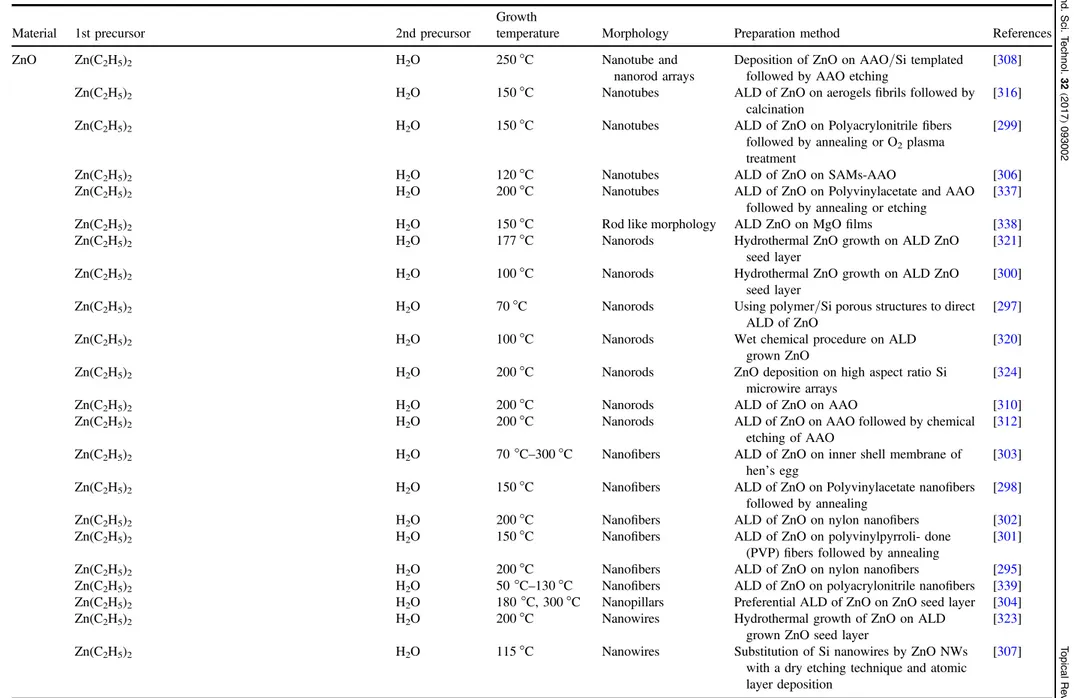
Quantum dots of semiconducting PbS(figure2) and CdS
have been synthesized by utilizing the incubation period observed during the initial stages of ALD where growth of islands is observed rather than formation of continuousfilms [288–290]. Note that this type of growth mode has only been
observed in certain ALD chemistries [288, 289]. This very
strategy of synthesizing quantum dots using ALD provides several unique advantages. Size of quantum dots can be varied by simply changing the number of growth cycles. Excellent infiltration of quantum dots can be obtained on high-surface area nanostructured templates by utilizing the high conformality of ALD processes. Moreover, as opposed to conventional quantum dot fabrication techniques, ALD eliminates the use of solutions and solution-based byproducts [288–290]. Islands with sub-10 nm diameters were observed
during the initial ALD cycles (10–40 growth cycles) of PbS on Si nanowire array(figure2) and PL measurements showed
a blue shift when number of ALD cycles are decreased confirming successful quantum confinement in PbS quantum dots(figure3) [290].
3.2. 1D structures
ALD grown 1D nanostructures are summarized in table 3. Majority of reports on ZnO nanostructures utilized nanoscale templates with the intention of disposing the template after deposition in order to obtain various kinds of ZnO
Figure 1.Various nanostructured templates used for template assisted ALD.(a) SEM image of nylon 6,6 polymeric nanofibers. (b) TEM image of single wall carbon nanotubes.(c) SEM image of porous AAO template. Reprinted with permission from [284,335]. Copyright
(2014, 2015) AIP publishing, Elsevier.
12
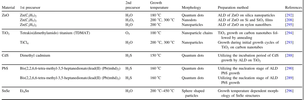
Table 2.Overview of the growth conditions employed to synthesize 0D nanostructures using ALD. The materials deposited, the morphology, precursors used, the temperature during ALD, and preparation method are mentioned.
Material 1st precursor
2nd precursor
Growth
temperature Morphology Preparation method References
ZnO Zn(C2H5)2 H2O 180°C Quantum dots ALD of ZnO on silica nanoparticles [292]
Zn(C2H5)2 H2O2 200°C, 300 °C Nanodots ALD of ZnO on Si and SiO2films [208]
Zn(C2H5)2 H2O 200°C Nanoparticles ALD of ZnO on nylon nanofibers [295]
TiO2 Tetrakis(dimethylamido) titanium (TDMAT) O3 100°C Nanoparticle chains TiO2growth on carbon nanotubes
fol-lowed by annealing
[294]
TiCl4 H2O 200°C, 300 °C Nanoparticles Growth during initial growth cycles of
TiO2on carbon nanotubes
[293]
CdS Dimethyl cadmium H2S 150°C Quantum dots Utilizing the incubation period of CdS
growth by ALD on TiO2
[288] PbS Bis(2,2,6,6-tetra-methyl-3,5-heptanedionato)lead(II) (Pb(tmhd)2) H2S 160°C Quantum dots Utilizing the nucleation stage of ALD
PbS growth
[290] Bis(2,2,6,6-tetra-methyl-3,5-heptanedionato)lead(II) (Pb(tmhd)2) H2S 160°C Quantum dots Utilizing the nucleation stage of ALD
PbS growth
[289]
SnSe Et4Sn H2O 200°C–450 °C Sphere shaped
particles
Growth temperature dependent morph-ology of SnSe structures
[296] 13 Semicond. Sci. T echnol. 32 (2017 ) 093002 T opical Re view
nanostructures [297–301]. Mainly three types of templates
have been used: anodized alumina (AAO) templates, poly-meric templates, and bio-nano-templates made out of biolo-gical materials [298, 301–304]. These templates have also
been used to study the conformality of ZnO as well as to
make multi-segmented ZnO nanotubes [305, 306]. ZnO
growth inside the pores of AAO was limited by precursor diffusion into the high aspect ratio wells and therefore long exposure times were necessary to obtain conformal coatings (120 s exposure time for aspect ratio of ∼5000) [305,306].
Moreover, with the utilized long exposure times, also exten-sive purging times were required to ensure the complete removal of the excess reactants and byproducts which will ensure the elimination of any unwanted gas-phase CVD reaction.
ZnO 1D structures such as nanorods or nanowires have been fabricated by utilizing lithography techniques or by performing growth directly on nanostructured templates [307–312]. In one study, combination of phase-shift
litho-graphy and plasma was utilized to synthesize a photoresist nanodot pattern on Si which was used to etch Si afterwards
Figure 2.TEM images of Si nanowires coated by ALD PbS shown at different magnifications after (a) 10 cycles, (b) 20 cycles, and (c) 40 cycles. Also shown is the effect of 20 min e-beam irradiation on the dot-coated Si nanowires.(As a result of the e-beam irradiation process, the crystallite morphology changes to a dome shape to lower the surface to volume ratio providing better contrast in TEM imaging.) Reprinted with permission from[290]. Copyright (2011) American Chemical Society.
Figure 3.Photoluminescence spectra for bare Si nanowires(blue), 10 cycles of ALD PbS(black), and 30 cycles of ALD PbS (red). Reprinted with permission from[290]. Copyright (2011) American
Chemical Society.
14
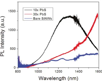
Table 3.Overview of the growth conditions employed to synthesize 1D nanostructures using ALD. The materials deposited, the morphology, precursors used, the temperature during ALD, and preparation method are mentioned.
Material 1st precursor 2nd precursor
Growth
temperature Morphology Preparation method References
ZnO Zn(C2H5)2 H2O 250°C Nanotube and
nanorod arrays
Deposition of ZnO on AAO/Si templated followed by AAO etching
[308]
Zn(C2H5)2 H2O 150°C Nanotubes ALD of ZnO on aerogelsfibrils followed by
calcination
[316]
Zn(C2H5)2 H2O 150°C Nanotubes ALD of ZnO on Polyacrylonitrilefibers
followed by annealing or O2plasma
treatment
[299]
Zn(C2H5)2 H2O 120°C Nanotubes ALD of ZnO on SAMs-AAO [306]
Zn(C2H5)2 H2O 200°C Nanotubes ALD of ZnO on Polyvinylacetate and AAO
followed by annealing or etching
[337]
Zn(C2H5)2 H2O 150°C Rod like morphology ALD ZnO on MgOfilms [338]
Zn(C2H5)2 H2O 177°C Nanorods Hydrothermal ZnO growth on ALD ZnO
seed layer
[321]
Zn(C2H5)2 H2O 100°C Nanorods Hydrothermal ZnO growth on ALD ZnO
seed layer
[300]
Zn(C2H5)2 H2O 70°C Nanorods Using polymer/Si porous structures to direct
ALD of ZnO
[297]
Zn(C2H5)2 H2O 100°C Nanorods Wet chemical procedure on ALD
grown ZnO
[320]
Zn(C2H5)2 H2O 200°C Nanorods ZnO deposition on high aspect ratio Si
microwire arrays
[324]
Zn(C2H5)2 H2O 200°C Nanorods ALD of ZnO on AAO [310]
Zn(C2H5)2 H2O 200°C Nanorods ALD of ZnO on AAO followed by chemical
etching of AAO
[312]
Zn(C2H5)2 H2O 70°C–300 °C Nanofibers ALD of ZnO on inner shell membrane of
hen’s egg [
303]
Zn(C2H5)2 H2O 150°C Nanofibers ALD of ZnO on Polyvinylacetate nanofibers
followed by annealing
[298]
Zn(C2H5)2 H2O 200°C Nanofibers ALD of ZnO on nylon nanofibers [302]
Zn(C2H5)2 H2O 150°C Nanofibers ALD of ZnO on polyvinylpyrroli- done
(PVP) fibers followed by annealing [301]
Zn(C2H5)2 H2O 200°C Nanofibers ALD of ZnO on nylon nanofibers [295]
Zn(C2H5)2 H2O 50°C–130 °C Nanofibers ALD of ZnO on polyacrylonitrile nanofibers [339]
Zn(C2H5)2 H2O 180°C, 300 °C Nanopillars Preferential ALD of ZnO on ZnO seed layer [304]
Zn(C2H5)2 H2O 200°C Nanowires Hydrothermal growth of ZnO on ALD
grown ZnO seed layer
[323]
Zn(C2H5)2 H2O 115°C Nanowires Substitution of Si nanowires by ZnO NWs
with a dry etching technique and atomic layer deposition [307] 15 Semicond. Sci. T echnol. 32 (2017 ) 093002 T opical Re view
Table 3.(Continued.)
Material 1st precursor 2nd precursor
Growth
temperature Morphology Preparation method References
Zn(C2H5)2 H2O 200°C Nanoneedles Hydrothermal growth of ZnO on ALD ZnO/
PAN nanofibers [
325]
Zn(C2H5)2 H2O 200°C Nanofibers ALD of ZnO on nylon nanofibers during
incubation period
[295]
TiO2 Titanium(IV) isopropoxide H2O 70°C Nanotubes TiO2growth into AAO membranes [326]
TiCl4 H2O 100°C Nanotubes TiO2growth into AAO membranes [328]
Titanium tetraisopropoxide H2O 150°C, 250 °C Nanotubes TiO2growth into AAO membranes and
carbon nanotubes
[327]
TiCl4 H2O 250°C Nanotubes TiO2growth on carbon nanotubes [329]
TiCl4 H2O 250°C–300 °C Nanotubes TiO2growth into AAO membranes [340]
TiCl4 H2O 150°C Nanotubes TiO2growth into AAO membranes [330]
TiCl4 H2O 600°C Nanorods TiO2growth into AAO membranes [341]
Ga2O3 Gallium(III) alkyl amidinate
[mono-acetamidinatodiethylgallium(III), compound 1]
H2O, O2 450°C Nanowires Self-seeding growth [342]
SnO2 SnCl4 H2O 150°C–400 °C Nanotubes SnO2growth into AAO membranes
fol-lowed by polishing and etching
[331]
Tin(IV) alkoxides Carboxylic
acid
75°C–250 °C Nanotubes SnO2growth on carbon nanotubes and boron
nitride nanotubes
[332]
SnCl4 H2O 200°C–400 °C Nanotubes SnO2growth on carbon nanotubes [343]
Tin tert-butoxide Acetic acid 200°C Nanotubes SnO2growth on carbon nanotubes [344]
GaN Ga(CH3)3 N2/H2plasma 200°C Flexible nanofibers GaN growth on electrospun nanofibers [285]
AlN Al2(CH3)6 NH3plasma 200°C Nanofibers GaN growth on electrospun nanofibers
fol-lowed by calcination
[333]
ZnS Zn(C2H5)2 H2S 75°C–180 °C Nanotubes ZnS growth on AAO template [334]
Cu2S Bis(N,N’-disec-butylacetamidinato)dicopper(I)
(CuAMD)
H2S 135°C Nanotubes ALD of Cu2S on single walled carbon
nanotubes
[335]
GaSx Ga2(NMe2)6 H2S 150°C Nanotubes ALD of GaSxon single walled carbon
nanotubes [336] 16 Semicond. Sci. T echnol. 32 (2017 ) 093002 T opical Re view
[307]. Another coating of photoresist and subsequent etching
of Si nanowires resulted in a mask for ALD of ZnO nano-wires. In another report, polymer templates synthesized through a combination of block copolymer lithography(BCL)
and nanoimprint lithography (NIL) were used as a
nano-template for subsequent ALD to obtain highly oriented and high-quality ZnO nanopatterns (illustration of fabrication steps are summarized infigure4) [297]. The fabricated
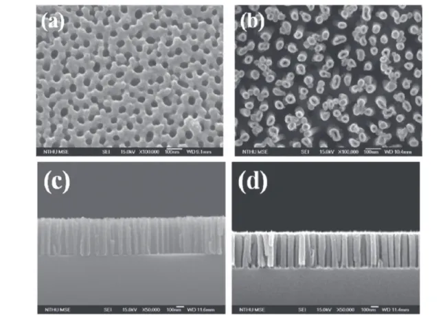
uni-form array of ZnO nanostructures possessed sub-100 nm feature and spatial resolutions, exhibiting narrow distributions in size and separation, and superior mechanical stability. AAO template has been commonly used for ZnO nanorod fabrication; AAO features long-range ordered vertically aligned nanopores with varying aspect ratios whose dimen-sions can be easily controlled by adjusting the process con-ditions[308,310,312,313]. It is a fairly simple technique to
obtain ZnO nanorods by growing on these templates followed by the removal process of AAO, usually accomplished by chemical wet etching. The pulse/exposure time of the pre-cursors needed to conformally coat inside the AAO pores is typically long as precursor molecules needs time to diffuse-in and react with the available adsorption sites within the high aspect ratio template walls.
Low temperature ALD of ZnO has enabled the use of bio-templates in ZnO nanostructuring. Cicada wings have been used as templates to fabricate ZnO nanopillars by taking advantage of the fact that nanopillars on the wing surface block ZnO growth[314,315]. Other studies utilized fibrils of hen’s
egg shell and nanocellulose fibers as bio-nanotemplates for ZnO coating [303, 316]. Figure 5 shows the fabricated ZnO nanotubes through bio templating; in this strategy,first nano-cellulose hydrogel is dried to aerogel, followed by coating with ZnO ALD to form composite organic/inorganic nanofibers, and finally calcinated to inorganic hollow nanotubes [316].
Peptide amphiphile nanofibrous templates were used as a soft template for ALD of ZnO and TiO2and resulting functional nanonetworks (figure 6) found applications in photocatalysis
for organic dye degradation and as anodic material in dye sensitized solar cells [317,318]. Overall, the use of
bio-tem-plates in ZnO nano-structuring is relatively less explored and thisfield might hold potential for future device applications.
There also are studies in which fabrication of ZnO nanorods or nanodots has been reported without using any templates. These studies take advantage of the incubation period of ZnO growth to form ZnO islands which can then be used as seeds for the growth of nanopillars[208,304,319]. In
some reports, ALD-grown ZnO thinfilms have been utilized
Figure 4.(i)–(v) Illustration of steps to fabricate ZnO nanoarrays using selective area ALD within templates defined by copolymer-derived NIL molds.(i) High-resolution silicon nanopillar molds (as shown in panel (a) as field effect scanning electron microscope (FESEM) image measured at 45° tilt). (ii) Nanoporous polymethylmethacrylate (PMMA) films obtained upon NIL (as shown in panel (b) by tapping mode atomic force microscope(AFM) image) and subsequently exposed to controlled O2plasma reactive ion etching(RIE) to obtain (iii) porous
templates with through-holes.(iv) ALD of ZnO on the nanoporous templates (as shown by FESEM image in panel (c)), followed by removal of templates to obtain(v) ZnO nanoarrays (as shown by tapping mode AFM image in panel (d)). Reprinted with permission from [297].
Copyright(2012) American Chemical Society.
17
as template for the subsequent growth of ZnO nanorods using hydrothermal process [320–324]. In these reports,
ALD-grown ZnO provides a high-quality texturedfilm to either act as a seed layer for nanorod growth or to protect the substrate from reagents of hydrothermal process. In another approach,
ALD ZnO coated polyacrylonitrile (PAN) nanofibers were
used as a template for over growth of ZnO nanoneedles via hydrothermal growth(figure7) [325].
Nanostructured TiO2 fabrication has been reported
mostly in the form of nanotubes and the most common pre-cursors utilized are TiCl4 and H2O [326–330]. Majority of
reports utilized AAO as a template for TiO2growth which
Figure 5.(a) A thin uniform ZnO layer formed on nanocellulose fibrils after initial exposure to the zinc precursor. (b) ZnO layer thickness is increased upon the ALD process(here 50 cycles). (c) Calcinated, hollow ZnO nanotubes are visibly rough. (d) Close-ups on ZnO nanotubes show that they are hollow. Reprinted with permission from[316]. Copyright (2011) American Chemical Society.
Figure 6.Characterization of as-synthesized TiO2and ZnO nanonetworks deposited with 350 and 100 ALD cycles, respectively.(a) and (b)
Scanning electron microscope(SEM) images, (c) energy dispersive x-ray spectroscopy (EDX) spectrum, and (d) XRD pattern of TiO2
nanonetworks.(e) and (f) SEM images, (g) EDX spectrum, and (h) XRD pattern of ZnO nanonetworks. Reprinted with permission from [318]. Copyright (2013) Nature publishing group.
18
was subsequently etched using NaOH solution to obtain TiO2 nanotubes[326–328]. Crystal morphology of TiO2nanotubes has been tuned from amorphous to anatase phase when
growth temperature was increased from 150°C to 250 °C
[327]. Figure8 shows TiO2nanotubes fabricated via titania deposition into AAO membranes followed by AAO removal through etching[328].
SnCl4and H2O precursors were employed to grow SnO2 nanotubes using AAO as a template followed by etching of AAO[331]. Interestingly, three temperature-dependent growth
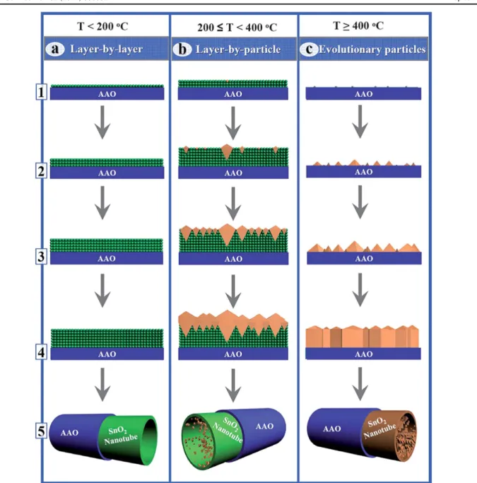
modes were observed(figure 9): (i) layer-by-layer growth at
temperature T<200 °C; (ii) layer-by-particle growth at temperature 200°CT<400 °C; (iii) evolutionary particles
at temperatures T 400 °C [331]. It was believed that
layer-by-layer growth occurred at low temperatures because of ligand exchange reactions and negligible change in reactive sites. Layer-by-particle growth occurred because of competing effects between ligand exchange and chlorination, i.e., lower growth temperatures prompt ligand exchange while higher temperatures can cause chlorination. Lastly, the evolutionary particle growth occurred at high growth temperatures mainly because of chlorination effects which caused certain nucleation sites on the substrate [331]. The layers were amorphous
whereas particles were identified as crystalline. Hence in this
way, morphology and phase of SnO2 nanotubes were
con-trolled via ALD growth temperature[331]. In another report it Figure 7.Representative SEM images of(a1 and 2) pristine PAN, (b1 and 2) PAN/ZnO seed, and (c1 and 2) PAN/ZnO needle nanofibers at different magnifications. Reprinted with permission from [325]. Copyright (2014) Elsevier.
19
![Table 2 provides a summary of ALD-grown 0D semi- semi-conductor nanostructures. ALD of ZnO has been carried out on SiO 2 film having nanoscale voids between them which allow subsequent deposition within the voids of the films [ 291, 292 ]](https://thumb-eu.123doks.com/thumbv2/9libnet/5605888.110595/12.892.78.817.96.322/provides-summary-conductor-nanostructures-carried-nanoscale-subsequent-deposition.webp)